 | –≠–ª–µ–∫—Ç—Ä–æ–Ω–Ω—ã–π –∫–æ–º–ø–æ–Ω–µ–Ω—Ç: BAT254/T1 | –°–∫–∞—á–∞—Ç—å:  PDF PDF  ZIP ZIP |
Document Outline
- FEATURES
- DESCRIPTION
- APPLICATIONS
- LIMITING VALUES
- ELECTRICAL CHARACTERISTICS
- GRAPHICAL DATA
- MOUNTING
- PACKAGE OUTLINE
- DEFINITIONS

DATA SHEET
Product specification
Supersedes data of 1996 Mar 19
1999 Apr 22
DISCRETE SEMICONDUCTORS
BAT254
Schottky barrier diode
dbook, halfpage
M3D154
1999 Apr 22
2
Philips Semiconductors
Product specification
Schottky barrier diode
BAT254
FEATURES
∑
Low forward voltage
∑
Guard ring protected
∑
Very small ceramic SMD package.
APPLICATIONS
∑
Ultra high-speed switching
∑
Voltage clamping
∑
Protection circuits
∑
Blocking diodes.
DESCRIPTION
Planar Schottky barrier diode encapsulated in a SOD110 very small ceramic
SMD package.
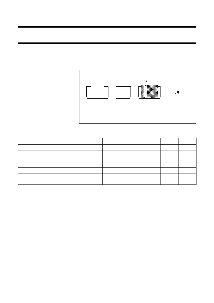
Fig.1 Simplified outline (SOD110) and symbol.
handbook, 4 columns
MAM214
k
a
cathode mark
top view
side view
bottom view
a
k
Marking code: L4.
LIMITING VALUES
In accordance with the Absolute Maximum Rating System (IEC 134).
SYMBOL
PARAMETER
CONDITIONS
MIN.
MAX.
UNIT
V
R
continuous reverse voltage
-
30
V
I
F
continuous forward current
-
200
mA
I
FRM
repetitive peak forward current
t
p
1 s;
0.5
-
300
mA
I
FSM
non-repetitive peak forward current
t
p
<
10 ms
-
600
mA
T
stg
storage temperature
-
65
+150
∞
C
T
j
junction temperature
-
125
∞
C
T
amb
operating ambient temperature
-
65
+125
∞
C

1999 Apr 22
3
Philips Semiconductors
Product specification
Schottky barrier diode
BAT254
ELECTRICAL CHARACTERISTICS
T
amb
= 25
∞
C unless otherwise specified.
Note
1. Pulse test: t
p
= 300
µ
s;
= 0.02.
THERMAL CHARACTERISTICS
Note
1. Refer to SOD110 standard mounting conditions.
SYMBOL
PARAMETER
CONDITIONS
MAX.
UNIT
V
F
forward voltage
see Fig.2
I
F
= 0.1 mA
240
mV
I
F
= 1 mA
320
mV
I
F
= 10 mA
400
mV
I
F
= 30 mA
500
mV
I
F
= 100 mA
800
mV
I
R
reverse current
V
R
= 25 V; note 1; see Fig.3
2
µ
A
t
rr
reverse recovery time
when switched from I
F
= 10 mA to
I
R
= 10 mA; R
L
= 100
; measured at
I
R
= 1 mA: see Fig.5
5
ns
C
d
diode capacitance
f = 1 MHz; V
R
= 1 V; see Fig.4
10
pF
SYMBOL
PARAMETER
CONDITIONS
VALUE
UNIT
R
th j-a
thermal resistance from junction to ambient
note 1
315
K/W

1999 Apr 22
4
Philips Semiconductors
Product specification
Schottky barrier diode
BAT254
GRAPHICAL DATA
handbook, halfpage
10
IF
VF (V)
3
10
(mA)
2
10
1
10
1
1.2
0.8
0.4
0
MSA892
(3)
(2)
(1)
(3)
(2)
(1)
(1) T
amb
= 125
∞
C.
(2) T
amb
= 85
∞
C.
(3) T
amb
= 25
∞
C.
Fig.2
Forward current as a function of forward
voltage; typical values.
0
10
20
30
V (V)
R
10
3
I
R
(
µ
A)
10
2
10
1
10
1
(1)
(2)
(3)
MSA893
(1) T
amb
= 125
∞
C.
(2) T
amb
= 85
∞
C.
(3) T
amb
= 25
∞
C.
Fig.3
Reverse current as a function of reverse
voltage; typical values.
0
10
20
30
0
5
10
15
V (V)
R
C d
(pF)
MSA891
f = 1 MHz; T
amb
= 25
∞
C.
Fig.4
Diode capacitance as a function of reverse
voltage; typical values.
Fig.5 Reverse recovery definitions.
handbook, halfpage
90%
10%
tf
Q
dI
dt
t
IF
IR
MRC129 - 1
F
r

1999 Apr 22
5
Philips Semiconductors
Product specification
Schottky barrier diode
BAT254
MOUNTING
Reflow soldering
Follow standard reflow soldering techniques to ensure
correct application of solder paste and placement of the
SOD110 package (see Fig.6).
Dimensions in mm.
Fig.6 SOD110 reflow soldering pattern.
handbook, halfpage
MGC119
,,
,,
,,,
,,,
3.00
1.25
1.00
1.00
,,
,,
,,,
,,,
Wave soldering
Before wave soldering, attach SOD110 packages to the
printed-circuit boards using a small dot of thermo-setting
epoxy or UV-curing adhesive centred between the
soldering lands (see Fig.7).
Dimensions in mm.
Fig.7 SOD110 wave soldering pattern.
handbook, halfpage
MGC126
,,
,,
3.40
1.25
1.10
,,
,,
,,,
,,,
1.10
,,,
,,,