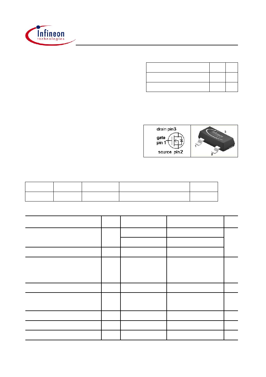
BSS139
SIPMOS
Æ
Small-Signal-Transistor
Features
∑ N-channel
∑ Depletion mode
∑ dv /dt rated
Maximum ratings, at T
j
=25 ∞C, unless otherwise specified
Parameter
Symbol Conditions
Unit
Continuous drain current
I
D
T
A
=25 ∞C
0.10
A
T
A
=70 ∞C
0.08
Pulsed drain current
I
D,pulse
T
A
=25 ∞C
0.4
Reverse diode dv /dt
dv /dt
I
D
=0.1 A, V
DS
=200 V,
di /dt =200 A/µs,
T
j,max
=150 ∞C
6
kV/µs
Gate source voltage
V
GS
±20
V
ESD sensitivity (HBM) as per
MIL-STD 883
Class 1
Power dissipation
P
tot
T
A
=25 ∞C
0.36
W
Operating and storage temperature
T
j
, T
stg
-55 ... 150
∞C
IEC climatic category; DIN IEC 68-1
55/150/56
Value
V
DS
250
V
R
DS(on),max
30
I
DSS,min
0.03
A
Product Summary
Type
Package
Ordering Code
Tape and Reel Information
Marking
BSS139
SOT-23
Q62702-S612
E6327: 3000 pcs/reel
STs
SOT-23
Rev. 1.0
page 1
2003-04-03

BSS139
Parameter
Symbol Conditions
Unit
min.
typ.
max.
Thermal characteristics
Thermal resistance,
junction - minimal footprint
R
thJA
-
-
350
K/W
Electrical characteristics, at T
j
=25 ∞C, unless otherwise specified
Static characteristics
Drain-source breakdown voltage
V
(BR)DSS
V
GS
=-3 V, I
D
=250 µA
250
-
-
V
Gate threshold voltage
V
GS(th)
V
DS
=3 V, I
D
=56 µA
-2.1
-1.4
-1
Drain-source leakage current
I
D (off)
V
DS
=250 V,
V
GS
=-3 V, T
j
=25 ∞C
-
-
0.1
µA
V
DS
=250 V,
V
GS
=-3 V, T
j
=125 ∞C
-
-
10
Gate-source leakage current
I
GSS
V
GS
=20 V, V
DS
=0 V
-
-
10
nA
Saturated drain current
I
DSS
V
GS
=0 V, V
DS
=10 V
30
-
-
mA
Drain-source on-state resistance
R
DS(on)
V
GS
=0 V, I
D
=15 mA
-
12.5
30
V
GS
=10 V, I
D
=0.1 A
-
7.8
14.0
Transconductance
g
fs
|V
DS
|>2|I
D
|R
DS(on)max
,
I
D
=0.08 A
0.06
0.13
-
S
Values
Rev. 1.0
page 2
2003-04-03
BSS139
Parameter
Symbol Conditions
Unit
min.
typ.
max.
Dynamic characteristics
Input capacitance
C
iss
-
60
76
pF
Output capacitance
C
oss
-
6.7
8.4
Reverse transfer capacitance
C
rss
-
2.6
3.3
Turn-on delay time
t
d(on)
-
5.8
8.7
ns
Rise time
t
r
-
5.4
8.1
Turn-off delay time
t
d(off)
-
29
43
Fall time
t
f
-
182
273
Gate Charge Characteristics
Gate to source charge
Q
gs
-
0.14
0.21
nC
Gate to drain charge
Q
gd
-
1.3
2.0
Gate charge total
Q
g
-
2.3
3.5
Gate plateau voltage
V
plateau
-
-0.28
-
V
Reverse Diode
Diode continous forward current
I
S
-
-
0.10
A
Diode pulse current
I
S,pulse
-
-
0.4
Diode forward voltage
V
SD
V
GS
=-3 V, I
F
=0.1 A,
T
j
=25 ∞C
-
0.81
1.2
V
Reverse recovery time
t
rr
-
8.6
12.9
ns
Reverse recovery charge
Q
rr
-
2.1
3.1
nC
V
R
=50 V, I
F
=0.04 A,
di
F
/dt =100 A/µs
T
A
=25 ∞C
Values
V
GS
=-3 V, V
DS
=25 V,
f =1 MHz
V
DD
=125 V,
V
GS
=-3...5 V,
I
D
=0.04 A, R
G
=6
V
DD
=200 V,
I
D
=0.04 A,
V
GS
=-3 to 5 V
Rev. 1.0
page 3
2003-04-03
BSS139
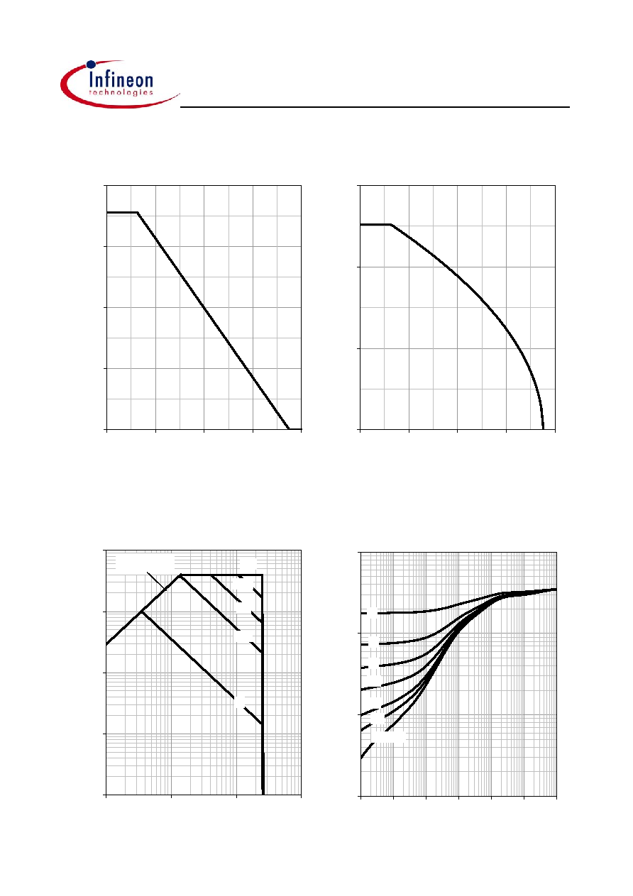
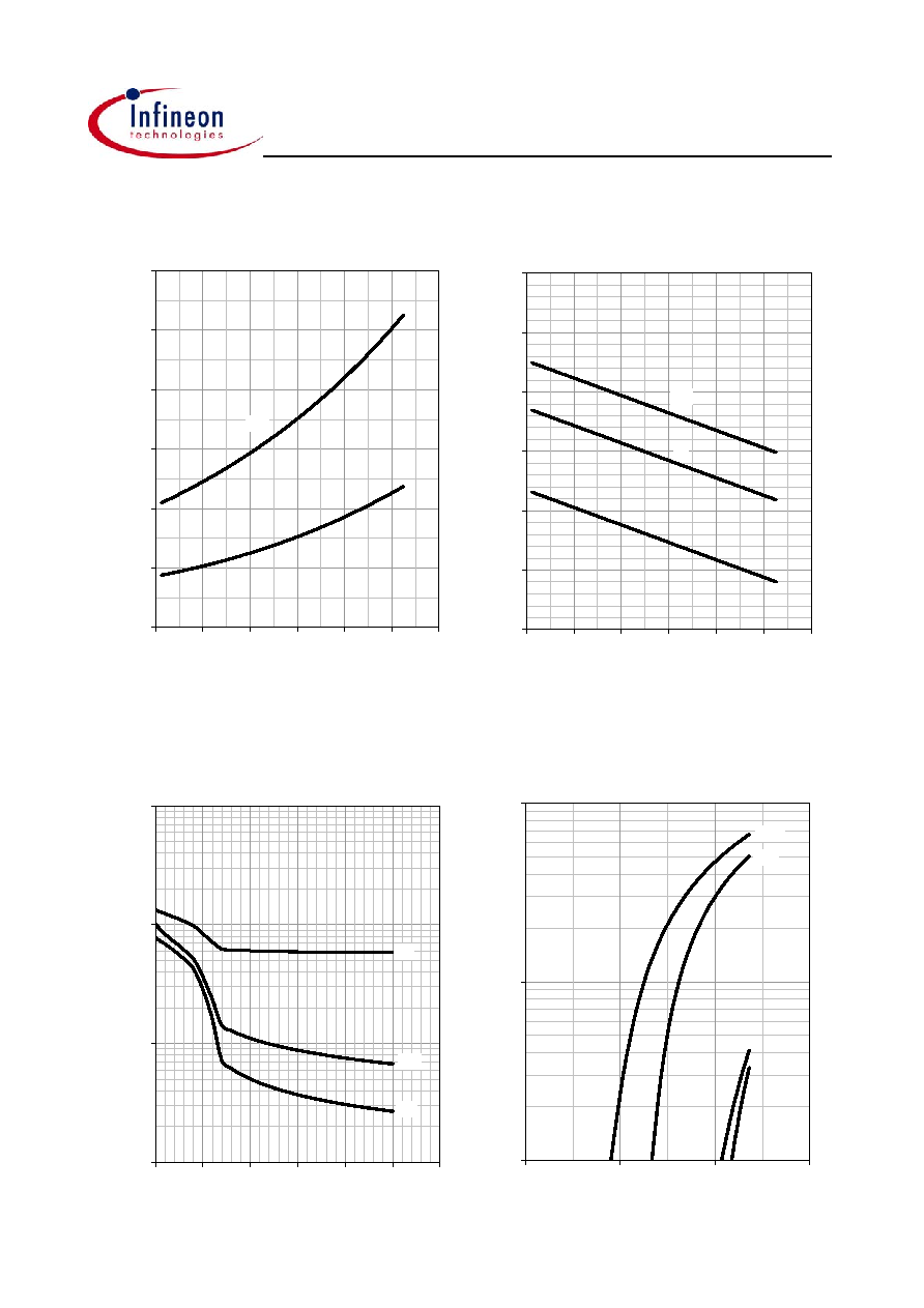
1 Power dissipation
2 Drain current
P
tot
=f(T
A
)
I
D
=f(T
A
); V
GS
10 V
3 Safe operation area
4 Max. transient thermal impedance
I
D
=f(V
DS
); T
A
=25 ∞C; D =0
Z
thJA
=f(t
p
)
parameter: t
p
parameter: D =t
p
/T
10 µs
100 µs
1 ms
10 ms
DC
0.0001
0.001
0.01
0.1
1
1
10
100
1000
V
DS
[V]
I
D
[A]
limited by on-state
resistance
single pulse
0.01
0.02
0.05
0.1
0.2
0.5
1
10
100
1000
0
0
0
0
1
10
100
t
p
[s]
Z
thJA
[K/W]
0
0.1
0.2
0.3
0.4
0
40
80
120
160
T
A
[∞C]
P
tot
[W]
0
0.04
0.08
0.12
0
40
80
120
160
T
A
[∞C]
I
D
[A]
10
-4
10
-3
10
-2
10
-1
10
0
10
1
10
2
Rev. 1.0
page 4
2003-04-03
BSS139
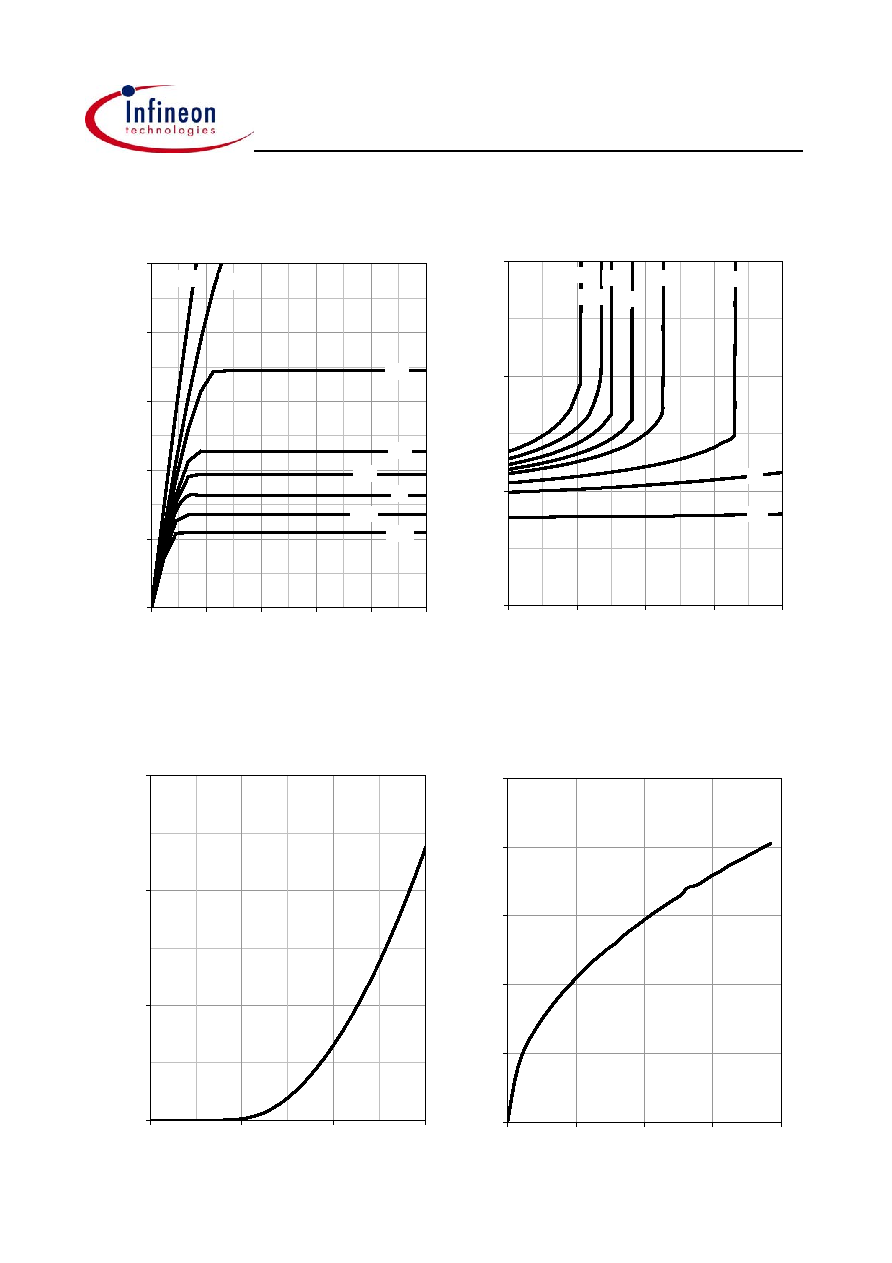
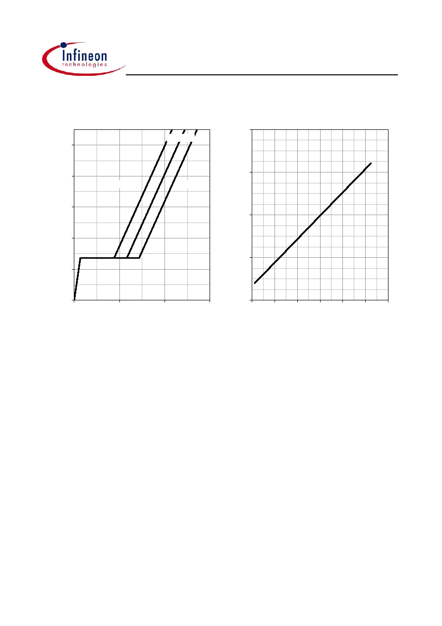
5 Typ. output characteristics
6 Typ. drain-source on resistance
I
D
=f(V
DS
); T
j
=25 ∞C
R
DS(on)
=f(I
D
); T
j
=25 ∞C
parameter: V
GS
parameter: V
GS
7 Typ. transfer characteristics
8 Typ. forward transconductance
I
D
=f(V
GS
); |V
DS
|>2|I
D
|R
DS(on)max
g
fs
=f(I
D
); T
j
=25 ∞C
-0.2 V
-0.1 V
0 V
0.1 V
0.2 V
0.5 V
1 V
10 V
0
10
20
30
0
0.04
0.08
0.12
0.16
I
D
[A]
R
D
S
(on)
[
]
0
0.1
0.2
0.3
-2
-1
0
1
V
GS
[V]
I
D
[A]
0
0.05
0.1
0.15
0.2
0.25
0.00
0.05
0.10
0.15
0.20
I
D
[A]
g
fs
[S]
-0.2 V
-0.1 V
0 V
0.1 V
0.2 V
0.5 V
1 V
10 V
0
0.04
0.08
0.12
0.16
0.2
0
2
4
6
8
10
V
DS
[V]
I
D
[A]
Rev. 1.0
page 5
2003-04-03
BSS139
9 Drain-source on-state resistance
10 Typ. gate threshold voltage
R
DS(on)
=f(T
j
); I
D
=0.015 A; V
GS
=0 V
V
GS(th)
=f(T
j
); V
DS
=3 V; I
D
=56 µA
parameter: I
D
11 Typ. Capacitances
12 Forward characteristics of reverse diode
C =f(V
DS
); V
GS
=-3 V; f =1 MHz
I
F
=f(V
SD
)
parameter: T
j
typ
98 %
0
10
20
30
40
50
60
-60
-20
20
60
100
140
180
T
j
[∞C]
R
D
S
(on)
[
]
typ
98 %
2 %
-3
-2.5
-2
-1.5
-1
-0.5
0
-60
-20
20
60
100
140
180
T
j
[∞C]
V
GS
(th)
[V]
Ciss
Coss
Crss
1
10
100
1000
0
5
10
15
20
25
30
V
DS
[V]
C
[pF]
25 ∞C
150 ∞C
25 ∞C, 98%
150 ∞C, 98%
0.01
0.1
1
0
0.5
1
1.5
V
SD
[V]
I
F
[A]
Rev. 1.0
page 6
2003-04-03
BSS139
14 Typ. gate charge
15 Drain-source breakdown voltage
V
GS
=f(Q
gate
); I
D
=0.04 A pulsed
V
BR(DSS)
=f(T
j
); I
D
=250 µA
parameter: V
DD
220
240
260
280
300
-60
-20
20
60
100
140
180
T
j
[∞C]
V
BR(
DSS)
[V]
0.2 VDS(max)
0.5 VDS(max)
0.8 VDS(max)
-3
-1
1
3
5
7
0
1
2
3
Q
gate
[nC]
V
GS
[V]
Rev. 1.0
page 7
2003-04-03
BSS139
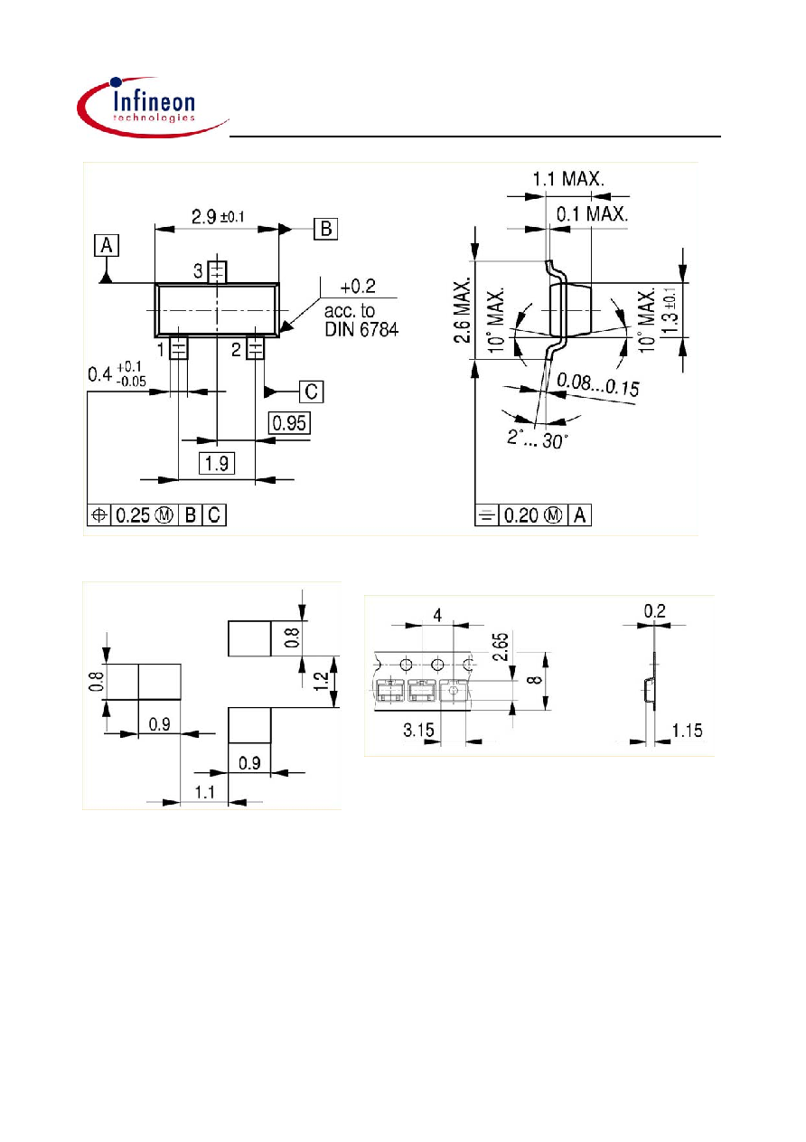
Package Outline:
Footprint:
Packaging:
Rev. 1.0
page 8
2003-04-03

BSS139
Published by
Infineon Technologies AG
Bereich Kommunikation
St.-Martin-Straþe 53
D-81541 M¸nchen
© Infineon Technologies AG 1999
All Rights Reserved.
Attention please!
The information herein is given to describe certain components and shall not be considered as
warranted characteristics.
Terms of delivery and rights to technical change reserved.
We hereby disclaim any and all warranties, including but not limited to warranties of non-infringement,
regarding circuits, descriptions and charts started herein.
Infineon Technologies is an approved CECC manufacturer.
Information
For further information on technology, delivery terms and conditions and prices, please contact your
nearest Infineon Technologies office in Germany or our Infineon Technologies representatives worldwide
(see address list).
Warnings
Due to technical requirements, components may contain dangerous substances.
For information on the types in question, please contact your nearest Infineon Technologies office.
Infineon Technologies' components may only be used in life-support devices or systems with the
expressed written approval of Infineon Technologies if a failure of such components can reasonably
be expected to cause the failure of that life-support device or system, or to affect the safety or
effectiveness of that device or system. Life support devices or systems are intended to be implanted
in the human body, or to support and/or maintain and sustain and/or protect human life. If they fail,
it is reasonable to assume that the health of the user or other persons may be endangered.
Rev. 1.0
page 9
2003-04-03