 | –≠–ª–µ–∫—Ç—Ä–æ–Ω–Ω—ã–π –∫–æ–º–ø–æ–Ω–µ–Ω—Ç: BTS737-S2 | –°–∫–∞—á–∞—Ç—å:  PDF PDF  ZIP ZIP |

BTS737S2
Infineon technologies
Page
1 of 1
2001-07-13
Smart High-Side Power Switch
with
ReverSave
Four Channels: 4 x 35m
Advanced Current Sense
Product Summary Package
Operating Voltage
V
bb(on)
4.5 ...40V
Active channels one
four parallel
On-state Resistance
R
ON
35m
9m
Nominal load current
I
L(NOM)
5.4A
11.1A
Current limitation
I
L(SCr)
21A
21A
General Description
∑ N channel vertical power MOSFET with charge pump, ground referenced CMOS compatible input and
diagnostic feedback, monolithically integrated in Smart SIPMOS
technology.
∑ Fully protected by embedded protection functions
Applications
∑ µC compatible high-side power switch with diagnostic feedback for 12V and 24V grounded loads
∑ All types of resistive and capacitve loads
∑ Most suitable for loads with high inrush currents, so as lamps
∑ Replaces electromechanical relays, fuses and discrete circuits
Basic Functions
∑ Very low standby current
∑ Improved electromagnetic compatibility (EMC)
∑ CMOS compatible input
∑ Stable behaviour at undervoltage
∑ Wide operating voltage range
Protection Functions
∑ Reverse battery protection without external components
(ReverSave
)
∑ Short circuit protection
∑ Overload
protection
∑ Current
limitation
∑ Thermal
shutdown
∑ Overvoltage protection (not load dump) without external
resistor
∑ Loss of ground protection
∑ Electrostatic discharge protection (ESD)
Diagnostic Function
∑
Proportional load current sense (with defined fault signal
during thermal shutdown)
Block Diagram
P-DSO-28
Vbb
Logic
Channel 3
Channel 4
GND
Load 1
Load 2
Logic
Channel 1
Channel 2
Load 4
Load 3
IN1
IS1
IS2
IN2
IN3
IS3
IS4
IN4

BTS737S2
Infineon technologies
Page 2
2001-07-13
Functional diagram
only active
in off-state
.
channel 1
OUT1
overvoltage
protection
logic
internal
voltage supply
ESD
temperature
sensor
clamp for
inductive load
gate
control
+
charge
pump
current limit
reverse
battery
protection
Proportional sense
current
control and protection circuit
of
channel 2
control and protection circuit
of
channel 3
control and protection circuit
of
channel 4
IN1
VBB
GND1/2
IN2
IN3
IN4
OUT2
OUT3
OUT4
LOAD
GND3/4
IS1
IS2
IS3
IS4
R 0

BTS737S2
Infineon technologies
Page 3
2001-07-13
Pin Definitions and Functions
Pin
Symbol
Function
1, 7, 8,
14,
15, 28
V
bb
Positive power supply voltage. Design the
wiring for the simultaneous max. short circuit
currents from channel 1 to 4 and also for low
thermal resistance
4
IN1
3
IN2
11
IN3
10
IN4
Input 1,2, 3,4 activates channel 1,2,3,4 in case
of logic high signal
25,26,27
OUT1
22,23,24
OUT2
19,20,21
OUT3
16,17,18
OUT4
Output 1,2,3,4 protected high-side power output
of channel 1,23,4. Design the wiring for the
max. short circuit current
5
IS1
6
IS2
12
IS3
13
IS4
Diagnostic feedback 1 .. 4 of channel 1 to 4
Providing a sense current, proportional to the
load current
2
GND1/2
Ground of chip 1 (channel 1,2)
9
GND3/4
Ground of chip 2 (channel 3,4)
Pin configuration
(top view)
V
bb
1
∑
28 V
bb
GND1/2
2
27 OUT1
IN2
3
26 OUT1
IN1
4
25 OUT1
IS1
5
24 OUT2
IS2
6
23 OUT2
V
bb
7
22 OUT2
V
bb
8
21 OUT3
GND3/4
9
20 OUT3
IN4
10
19 OUT3
IN3
11
18 OUT4
IS3
12
17 OUT4
IS4
13
16 OUT4
V
bb
14
15 V
bb

BTS737S2
Infineon technologies
Page 4
2001-07-13
Maximum Ratings
at T
j
= 25∞C unless otherwise specified
Parameter
Symbol
Values
Unit
Supply voltage (overvoltage protection see page 6)
V
bb
43
V
Supply voltage for full short circuit protection
T
j,start
=
-40 ...+150∞C
V
bb
36
V
Load current (Short-circuit current, see page 6)
I
L
self-limited
A
Load dump protection
1)
V
LoadDump
= V
A
+ V
s
, V
A
= 13.5 V
R
I
2)
= 2
, t
d
= 400
ms; IN
= low or high,
each channel loaded with R
L
=
4.7
,
V
Load
dump
3
)
60
V
Operating temperature range
Storage temperature range
T
j
T
stg
-40 ...+150
-55 ...+150
∞C
Power dissipation (DC)
4)
T
a
= 25∞C:
(all channels active)
T
a
= 85∞C:
P
tot
3.7
1.9
W
Maximal switchable inductance, single pulse
V
bb
=
12V, T
j,start
=
150∞C
4)
,
I
L
=
4.0
A, E
AS
=
0.8J, 0
one channel:
I
L
=
6.0
A, E
AS
=
1.0J, 0
two parallel channels:
I
L
=
9.5
A, E
AS
=
1.5J, 0
four parallel channels:
see diagrams on page 11
Z
L
33
37
64
mH
Electrostatic discharge capability (ESD)
IN:
(Human Body Model)
IS:
out to all other pins shorted:
acc. MIL-STD883D, method 3015.7 and ESD assn. std. S5.1-1993
R=1.5k
; C=100pF
V
ESD
1.0
4.0
8.0
kV
Input voltage (DC)
V
IN
-10 ... +16
V
Current through input pin (DC)
Current through sense pin (DC)
see internal circuit diagram page 10
I
IN
I
IS
±0.3
±0.3
mA
1)
Supply voltages higher than V
bb(AZ)
require an external current limit for the GND and status pins (a 75
resistor for the GND connection is recommended.
2)
R
I
= internal resistance of the load dump test pulse generator
3)
V
Load dump
is setup without the DUT connected to the generator per ISO 7637-1 and DIN 40839
4)
Device on 50mm*50mm*1.5mm epoxy PCB FR4 with 6cm
2
(one layer, 70
µm thick) copper area for Vbb
connection. PCB is vertical without blown air. See page 16

BTS737S2
Infineon technologies
Page 5
2001-07-13
Thermal Characteristics
Parameter and Conditions
Symbol
Values
Unit
min
typ
Max
Thermal resistance
junction - soldering point
5)6),
each channel:
R
thjs
--
--
11
K/W
junction ≠ ambient
6)
@ 6 cm
2
cooling area
one channel active:
all channels active:
R
thja
--
--
40
33
--
--
Electrical Characteristics
Parameter and Conditions,
each of the four channels
Symbol
Values
Unit
at T
j
= -40...+150∞C, V
bb
= 12 V unless otherwise specified
min
typ
Max
Load Switching Capabilities and Characteristics
On-state resistance (Vbb to OUT);
IL = 5 A, V
bb
7V
each channel, T
j
= 25∞C:
T
j
= 150∞C:
two parallel channels, T
j
= 25∞C:
four parallel channels, T
j
= 25∞C:
see diagram, page 12
R
ON
--
--
--
--
30
55
15
8
35
64
18
9
m
Nominal load current
one channel active:
two parallel channels active:
four parallel channels active:
Device on PCB
6)
, Ta = 85∞C, Tj 150∞C
I
L(NOM)
5.0
6.7
10.5
5.4
7.4
11.1
--
--
--
A
Output current
while GND disconnected
, VIN = 0,
see diagram page 11; (not tested specified by design)
I
L(GNDhigh)
--
--
1
mA
Turn-on time
7)
IN
to 90% V
OUT
:
Turn-off time
IN
to 10% V
OUT
:
R
L
=
12
t
on
t
off
--
--
50
120
150
220
µs
Slew rate on
7)
10 to 30% V
OUT
,
R
L
=
12
:
dV/dt
on
0.3
--
1
V/
µs
Slew rate off
7)
70 to 40% V
OUT
, R
L
=
12
:
-dV/dt
off
0.15
--
1
V/
µs
5)
Soldering point: upper side of solder edge of device pin 7,8. See page 16.
6)
Device on 50mm*50mm*1.5mm epoxy PCB FR4 with 6cm
2
(one layer, 70
µm thick) copper area for Vbb
connection. PCB is vertical without blown air. See page 16
7)
See timing diagram on page 13.

BTS737S2
Parameter and Conditions,
each of the four channels
Symbol
Values
Unit
at T
j
= -40...+150∞C, V
bb
= 12 V unless otherwise specified
min
typ
Max
Infineon technologies
Page 6
2001-07-13
Operating Parameters
Operating voltage
V
bb(on)
4.5
--
40
V
Overvoltage protection
8)
I
bb
=
40 mA
V
bb(AZ)
41
47
52
V
Standby current
9)
T
j
=-40...25∞C
:
V
IN
=
0;
see diagram page 12
T
j
=150∞C:
I
bb(off)
--
--
10
40
25
80
µA
not tested, specified by design: T
j
=125∞C:
--
25
Off-State output current
T
j
=-40...25∞C:
(included in I
bb(off)
)V
IN
=
0; each channel;T
j
=150∞C
:
I
L(off)
--
--
1
--
4
15
µA
Operating current, V
IN
=
5V,
I
GND
= I
GND1/2
+ I
GND3/4
,
one channel on:
four channels on:
I
GND
--
--
1.6
6.0
--
--
mA
Protection Functions
10)
Current limit,
(see timing diagrams, page 14)
I
L(lim)
36
45
58
A
Repetitive short circuit current limit,
T
j
= T
jt
each channel
two,three or four parallel channels
(see timing diagrams, page 14)
I
L(SCr)
--
--
40
40
--
--
A
Initial short circuit shutdown time
T
j,start
=25∞C:
(see timing diagrams on page 14)
t
off(SC)
--
4
--
ms
Output clamp (inductive load switch off)
11)
at VON(CL) = Vbb - VOUT
,
IL= 40 mA
T
j
=-40∞C..25∞C:
T
j
=150∞C:
V
ON(CL)
18
14
21
17
30
20
V
Thermal overload trip temperature
T
jt
150
--
--
∞C
Thermal hysteresis
T
jt
--
10
--
K
8)
Supply voltages higher than V
bb(AZ)
require an external current limit for the GND and status pins (a 150
resistor for the GND connection is recommended). See also V
ON(CL)
in table of protection functions and
circuit diagram on page 10.
9)
Measured with load; for the whole device; all channels off
10)
Integrated protection functions are designed to prevent IC destruction under fault conditions described in the
data sheet. Fault conditions are considered as "outside" normal operating range. Protection functions are not
designed for continuous repetitive operation.
11)
If channels are connected in parallel, output clamp is usually accomplished by the channel with the lowest
V
ON(CL)

BTS737S2
Parameter and Conditions,
each of the four channels
Symbol
Values
Unit
at T
j
= -40...+150∞C, V
bb
= 12 V unless otherwise specified
min
typ
Max
Infineon technologies
Page 7
2001-07-13
Reverse Battery
Reverse battery voltage
12)
-V
bb
--
--
28
V
On-state resistance with reverse battery
IL = 2A; Vbb = 12V
Tj =25∞C:
Tj =150∞C:
R
on
--
--
45
80
60
120
m
Input
13)
Input resistance
(see circuit page 10)
R
I
2.5
3.5
6.0
k
Input turn-on threshold voltage
V
IN(T+)
1.7
--
3.2
V
Input turn-off threshold voltage
V
IN(T-)
1.5
--
--
V
Input threshold hysteresis
V
IN(T)
--
0.3
--
V
Off state input current
V
IN
= 0.4 V:
I
IN(off)
1
--
35
µA
On state input current
V
IN
= 5 V:
I
IN(on)
20
50
90
µA
12)
Power dissipation is higher compared to normal operating conditions due to the elevated on-state reistance.
The temperature protection and sense functionality is not active during reverse current operation! Input and
Status currents have to be limited (see max. ratings page 4 and circuit page 10).
13)
If ground resistors R
GND
are used, add the voltage drop across these resistors.

BTS737S2
Parameter and Conditions,
each of the four channels
Symbol
Values
Unit
at T
j
= -40...+150∞C, V
bb
= 12 V unless otherwise specified
min
typ
Max
Infineon technologies
Page 8
2001-07-13
Diagnostic Characteristics
Current sense ratio, static on-condition,
kILIS =IL:IIS
k
ILIS
--
5 000
--
-40∞C
I
L
=
10
A:
I
L
=
2
A:
I
L
=
1
A:
I
L
=
0.5
A:
4575
4100
4200
3580
5000
5000
5200
5800
5425
5900
6200
8080
+25∞C
I
L
=
10
A:
I
L
=
2
A:
I
L
=
1
A:
I
L
=
0.5
A:
4600
4250
4310
3820
4900
4900
5100
5600
5200
5550
6010
7320
+150∞C
I
L
=
10
A:
I
L
=
2
A:
I
L
=
1
A:
I
L
=
0.5
A:
4675
4475
4350
4200
4900
4900
5000
5200
5125
5325
5650
6200
Sense signal in case of fault-conditions
14)
V
fault
5.8
6.3
6.9
V
Sense signal delay after thermal shutdown
15)
t
delay(fault)
--
--
1
ms
Sense current saturation
I
IS,lim
4
--
--
mA
Current sense output voltage limitation
I
IS
= 0, I
L
= 5 A:
V
IS(lim)
5.8
6.3
6.9
V
Current sense leakage/offset current
V
IN
=0, V
IS
= 0, I
L
= 0:
I
IS(LL)
--
--
1
µA
V
IN
=5 V, V
IS
= 0, I
L
= 0:
I
IS(LH)
--
2.5
--
Current sense settling time to I
IS static
±10% after
positive input slope, I
L
= 0
5 A,
(not tested, specified by design)
t
son(IS)
--
--
300
µs
Internal output pull down
only active in off-state
R
0
--
7
--
k
14)
In the case of current limitation or thermal shutdown the sense signal is no longer a current proportional to
the load current, but a fixed voltage of typ. 5 V.
15)
In the case of thermal shutdown the V
fault
signal remains for t
delay(fault)
longer than the restart of the switch (see
diagram on page 15).

BTS737S2
Infineon technologies
Page 9
2001-07-13
Truth Table
Input
level
Output
level
Current
Sense
I
IS
Normal
Operation
L
H
L
H
0
nominal
Current-
Limitation
16)
H
H
V
fault
Short circuit to GND
L
H
L
L
0
V
fault
Overtemperature
L
H
L
L
0
V
fault
Short circuit to V
bb
L
H
H
H
0
<nominal
17)
Open load
L
H
Z
H
0
0
Negative output
Voltage clamp
L
L
0
L = "Low" Level
X = don't care
Z = high impedance, potential depends on external circuit
H = "High" Level
V
fault
= 5V typ, constant voltage independent of external used sense resistor.
Parallel switching of channels is possible by connecting the inputs and outputs in parallel. The current sense
outputs have to be connected with a single sense resistor.
Terms
PROFET
OUT2
GND1/2
OUT1
Chip 1
V
bb
PROFET
OUT4
GND3/4
OUT3
Chip 2
V
bb
Leadframe
3
IN 1
I
IN1
IN 2
5
I
IN2
IS1
2
I
IS1
IS2
6
I
IS2
V
IN1
V
bb
4
I
IGND1/2
I
bb
25
26
27
22
23
24
V
ON1
V
ON2
I
L1
I
L2
V
OUT1
V
OUT2
V
IS1
V
IS2
V
IN2
Leadfram e
10
IN 3
I
IN3
IN 4
12
I
IN4
IS3
9
I
IS3
IS4
13
I
IS4
V
IN3
V
bb
11
I
IGND3/4
19
20
21
16
17
18
V
ON3
V
ON4
I
L3
I
L4
V
OUT3
V
OUT4
V
IS3
V
IS4
V
IN4
Leadframe (V
bb
) is connected to pin 1, 7, 8, 14, 15, 28
.
16)
Current limitation is only possible while the device is switched on.
17)
Low ohmic short to
V
bb
may reduce the output current
I
L
and therefore also the sense current
I
IS
.

BTS737S2
Infineon technologies
Page 10
2001-07-13
Input circuit (ESD protection),
IN1 to IN4
IN
GND
I
R
ESD-ZD
I
I
I
The use of ESD zener diodes as voltage clamp at DC
conditions is not recommended.
Sense output
Normal operation: I
S
= I
L
/ k
ILIS
V
IS
=
I
S *
R
IS
; R
IS
= 1 k
nominal
R
IS
> 500
IS
GND
IS
R
IS
I
ESD-ZD
IS
V
V
f
Sense output
logic
ESD-Zener diode: V
ESD
= 6.1 V typ., max 14 mA;
Operation under fault condition
so as thermal shut down or current limitation
GND
IS
R
ESD-ZD
V
fault
V
fault
V
f
Sense output
logic
V
fault
= 6V typ
V
fault
<
V
ESD under all conditions
Overvoltage output clamp,
OUT1 or OUT2
+Vbb
OUT
VZ
V
ON
Power GND
V
ON
clamped to V
ON(CL)
= 21 V typ.
Overvoltage protection of logic part
GND1/2 or GND3/4
+ Vbb
IS
IS
R
GND
Integrated
GND resistor
RGND
Signal GND
Logic
VZ2
IN
RI
V
Z1
V
Z1
=
6.1
V typ., V
Z2
=
47
V typ., R
I
=
3.5
k
typ.,
R
GND
= 75
Reverse battery protection
Logic
IS
R
IN
IS
OUT
L
R
Power GND
Integrated
GND resistor
RGND
Signal GND
Power
MOSFET
I
R
Vbb
-
Logic
MOSFET
R
GND
= 75
, R
I
= 3.5 k
typ,
In case of reverse battery the channel of the MOSFET is
turned on.
Temperature protection and sense functionality is not active
during inverse current operation.
BTS737S2
Infineon technologies
Page 11
2001-07-13
GND disconnect
PROFET
V
IN
IS
OUT
GND
bb
V
bb
V
IN
V
ST
V
GND
Any kind of load. In case of IN
=
high is V
OUT
V
IN
-
V
IN(T+)
.
Due to V
GND
>
0, no V
ST
= low signal available.
V
bb
disconnect with energized inductive
load
PROFET
V
IN
IS
OUT
GND
bb
V
bb
high
For inductive load currents up to the limits defined by Z
L
(max. ratings and diagram on page 11) each switch is
protected against loss of Vbb.
Consider at your PCB layout that in the case of Vbb dis-
connection with energized inductive load all the load current
flows through the GND connection.
Inductive load switch-off energy
dissipation
PROFET
V
IN
IS
OUT
GND
bb
=
E
E
E
EAS
bb
L
R
ELoad
RL
L
{
L
Z
Energy stored in load inductance:
E
L
=
1/2
∑
L
∑
I
2
L
While demagnetizing load inductance, the energy
dissipated in PROFET is
E
AS
= E
bb
+ E
L
- E
R
= V
ON(CL)
∑
i
L
(t) dt,
with an approximate solution for RL > 0
:
E
AS
=
I
L
∑
L
2
∑
R
L
(
V
bb
+
|V
OUT(CL)
|)
ln
(1+
I
L
∑
R
L
|V
OUT(CL)
|
)
Maximum allowable load inductance for
a single switch off
(one channel)
4)
L = f (IL ); Tj,start =
150∞C, Vbb =
12
V, RL =
0
ZL [mH]
1
10
100
1000
0
1
2
3
4
5
6
7
0.1
IL [A]

BTS737S2
Infineon technologies
Page 12
2001-07-13
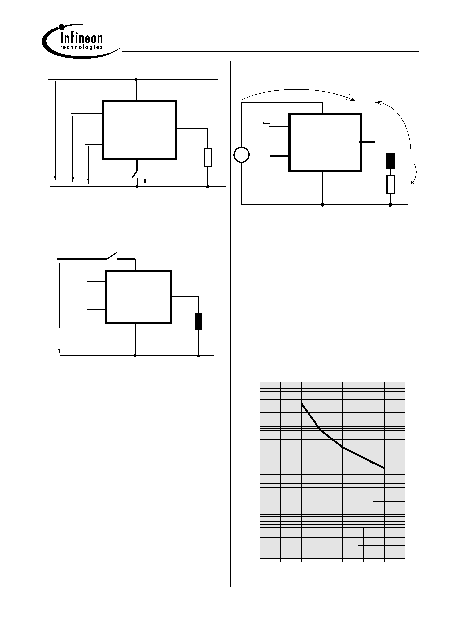
Typ. on-state resistance
R
ON
= f (Vbb,Tj ); I
L
=
2
A, IN
= high
R
ON
[mOhm]
60
50
180
30
20
0
3 5 7 9
30
40
Tj = 150∞C
25∞C
-40∞C
V
bb
[V]
Typ. standby current
I
bb(off)
= f (T
j
); V
bb
= 9...34 V, IN1,2,3,4
= low
I
bb(off)
[
µA]
0
5
10
15
20
25
30
35
40
45
-50
0
50
100
150
200
T
j
[∞C]

BTS737S2
Infineon technologies
Page 13
2001-07-13
Figure 1a: Switching a resistive load,
change of load current in on-condition:
IN
OUT
L
t
V
I
I
S
,V
S
t
son(IS)
t
t
slc(IS)
slc(IS)
Load 1
Load 2
soff(IS)
t
t
t
on
off
The sense signal is not valid during settling time after turn on or
change of load current.
Figure 1b: V
bb
turn on:
IN
V
L
I
bb
I
S
,V
S
proper turn on under all conditions
Figure 1c: Behaviour of sense output:
Sense current (I
S
) and sense voltage (V
S
) as
function of load current dependent on the sense
resistor
Shown is V
S
and I
S
for three different sense
resistors. Curve 1 refers to a low resistor, curve 2 to
a medium-sized resistor and curve 3 to a big resistor.
Note, that the sense resistor may not fall short of a
minimum value of 500
.
V
S
I
L(lim)
V
fault
V
ESD
I
S
I
L
I
L
1
2
1
3
2
3
I
S
= I
L
/ k
ILIS
V
IS
=
I
S *
R
IS
; R
IS
= 1 k
nominal
R
IS
> 500
Functionality diagrams
All diagrams are shown for chip 1 (channel 1/2). For chip 2 (channel 3/4) the diagrams are valid too. The
channels 1 and 2, respectively 3 and 4, are symmetric and consequently the diagrams are valid for each
channel as well as for permuted channels

BTS737S2
Infineon technologies
Page 14
2001-07-13
Figure 2a: Switching a lamp:
IN
ST
OUT
L
t
V
I
The initial peak current should be limited by the lamp and not by the
current limit of the device.
Figure 2b: Switching a lamp with current limit:
The behaviour of IS and VS is shown for a resistor,
which refers to curve 1 in figure 1c
IN
OUT
L
t
V
I
I
S
V
S
V
fault
Figure 3a: Short circuit:
shut down by overtempertature, reset by cooling
IN
I
L(SCr)
I
IL(lim)
L
V
S
V
fault
Heating up may require several milliseconds, depending on
external conditions
I
LL(lim')
= 50 A typ. increases with decreasing temperature.
Figure 3b: Turn on into short circuit:
shut down by overtemperature, restart by cooling
(two parallel switched channels 1 and 2)
IN1/2
L(SCr)
I
IL1 + IL2
IL(SCp)
toff(SC)
V
S1
, V
S2
V
fault

BTS737S2
Infineon technologies
Page 15
2001-07-13
Figure 4a: Overtemperature:
Reset if T
j
<T
jt
The behaviour of IS and VS is shown for a resistor,
which refers to curve 1 in figure 1c
t
IN
IL
V
S
T
J
I
S
t
delay(fault)
V
fault
Figure 6a: Current sense versus load current:
0
0.1
0.2
0.3
0.4
0.5
0.6
0.7
0.8
0.9
1
1.1
1.2
1.3
0
1
2
3
4
5
6
I L
[A]
[mA]
IIS
Figure 6b: Current sense ratio
18)
:
0
5000
10000
0 1 2 3 4 5 6 7 8 9 10 11 12 13
IL
[A]
kILIS
18)
This range for the current sense ratio refers to all
devices. The accuracy of the
k
ILIS
can be raised at
least by a factor of two by calibrating the value of
k
ILIS
for every single device.

BTS737S2
Infineon technologies
Page 16
2001-07-13
Package and Ordering Code
Standard: P-DSO-28-16
Sales Code
BTS 737 S2
Ordering Code
Q67060-S7017
1
14
15
28
18.1
-0.4
Index Marking
1)
2.45
-0.1
7.6
10.3
±0.3
-0.2
0.2
2.65 max
-0.2
1.27
0.23
+0.09
0.1
0.4
0.35 x 45∞
+0.8
+0.15
0.35
2)
8∞ max
0.2 28x
1)
2) Does not include dambar protrusion of 0.05 max per side
1) Does not include plastic or metal protrusions of 0.15 max rer side
GPS05123
All dimensions in millimetres
Definition of soldering point with temperature T
s
:
upper side of solder edge of device pin 15.
Pin 7,8
Printed circuit board (FR4, 1.5mm thick, one layer
70
µm, 6cm
2
active heatsink area) as a reference for
max. power dissipation P
tot
, nominal load current
I
L(NOM)
and thermal resistance R
thja
Published by Infineon technologies AG, Bereich Bauelemente,
Vertrieb, Produkt-Information, Balanstraþe 73, D-81541
M¸nchen
Infineon technologies AG 2001. All Rights Reserved
As far as patents or other rights of third parties are concerned,
liability is only assumed for components per se, not for applications,
processes and circuits implemented within components or assem-
blies. The information describes a type of component and shall not
be considered as warranted characteristics. The characteristics for
which SIEMENS grants a warranty will only be specified in the
purchase contract. Terms of delivery and rights to change design
reserved. For questions on technology, delivery and prices please
contact the Offices of Semiconductor Group in Germany or the
Siemens Companies and Representatives woldwide (see address
list). Due to technical requirements components may contain dan-
gerous substances. For information on the type in question please
contact your nearest Infineon technologies AG Office,
Semiconductor Group. Siemens AG is an approved CECC
manufacturer.
Packing: Please use the recycling operators known to you. We can
also help you - get in touch with your nearest sales office. By
agreement we will take packing material back, if it is sorted. You
must bear the costs of transport. For packing material that is re-
turned to us unsorted or which we are not obliged to accept we shall
have to invoice you for any costs incurred.
Components used in life-support devices or systems must be
expressly authorised for such purpose! Critical components19
)
of
the Semiconductor Group of Infineon technologies AG, may only be
used in life supporting devices or systems20
)
with the express
written approval of the Semiconductor Group of Infineon
technologies AG.
19) A critical component is a component used in a life-support
device or system whose failure can reasonably be expected to
cause the failure of that life-support device or system, or to
affect its safety or effectiveness of that device or system.
20) Life support devices or systems are intended (a) to be
implanted in the human body or (b) support and/or maintain
and sustain and/or protect human life. If they fail, it is
reasonably to assume that the health of the user or other
persons may be endangered.