N e v e r s t o p t h i n k i n g .
H Y B 1 8 L 2 5 6 1 6 0 B [ C / F ] - 7 . 5
H Y E 1 8 L 2 5 6 1 6 0 B [ C / F ] - 7 . 5
H Y E 1 8 L 2 5 6 1 6 0 B C L - 7 . 5
H Y E 1 8 L 2 5 6 1 6 0 B F L - 7 . 5
D R A M s f o r M o b i l e A p p l i c a t i o n s
2 5 6 - M b i t M o b i l e - R A M
D a t a S h e e t , R e v . 1 . 7 2 , J u l y 2 0 0 5
M e m o r y P r o d u c t s

Edition 2005-07
Published by Infineon Technologies AG,
St.-Martin-Strasse 53,
81669 M¸nchen, Germany
©
Infineon Technologies AG 2005.
All Rights Reserved.
Attention please!
The information herein is given to describe certain components and shall not be considered as a guarantee of
characteristics.
Terms of delivery and rights to technical change reserved.
We hereby disclaim any and all warranties, including but not limited to warranties of non-infringement, regarding
circuits, descriptions and charts stated herein.
Information
For further information on technology, delivery terms and conditions and prices please contact your nearest
Infineon Technologies Office (
www.infineon.com
).
Warnings
Due to technical requirements components may contain dangerous substances. For information on the types in
question please contact your nearest Infineon Technologies Office.
Under no circumstances may the Infineon Technologies product as referred to in this data sheet be used in
1. Any applications that are intended for military usage (including but not limited to weaponry), or
2. Any applications, devices or systems which are safety critical or serve the purpose of supporting, maintaining,
sustaining or protecting human life (such applications, devices and systems collectively referred to as "Critical
Systems"), if
a) A failure of the Infineon Technologies product can reasonable be expected to - directly or indirectly -
(i) Have a detrimental effect on such Critical Systems in terms of reliability, effectiveness or safety; or
(ii) Cause the failure of such Critical Systems; or
b) A failure or malfunction of such Critical Systems can reasonably be expected to - directly or indirectly -
(i) Endanger the health or the life of the user of such Critical Systems or any other person; or
(ii) Otherwise cause material damages (including but not limited to death, bodily injury or significant
damages to property, whether tangible or intangible).

HY[B/E]18L256160B[C/F]L-7.5
256-Mbit Mobile-RAM
Data Sheet
3
Rev. 1.72, 2005-07
01302004-CZ2R-J9SE
HYB18L256160B[C/F]-7.5 HYE18L256160B[C/F]-7.5 HYE18L256160BCL-7.5 HYE18L256160BFL-7.5
Revision History:
Rev. 1.72
2005-07
Previous Revision:
2
added disclaimer
48
Rev.1.71: deleted -BCX and BFX product types (R-05-0635)
2005-07-15
Rev.1.61
28
Figure 25
: Updated
12
Chapter 2.1
: added to note 6: Programming of the Extended Mode Register...
14
Extended Mode Register table: Editorial changes
Chapter 2.2.1.6
: Editorial change
38
Chapter 2.4.9.2
: replaced last paragraph by: If during normal operation...
17
,
28
,
44
,
45 Table 7
,
Table 11
and
Table 20
: t
IH
changed
Table 20
: note 7 changed: If
t
T
> 1ns, a value of [0.5 x (tT -1)] ns...
Table 19
: editorial changes
We Listen to Your Comments
Any information within this document that you feel is wrong, unclear or missing at all?
Your feedback will help us to continuously improve the quality of this document.
Please send your proposal (including a reference to this document) to:
techdoc.mp@infineon.com

Data Sheet
4
Rev. 1.72, 2005-07
HY[B/E]18L256160B[C/F]L-7.5
256-Mbit Mobile-RAM
1
Overview . . . . . . . . . . . . . . . . . . . . . . . . . . . . . . . . . . . . . . . . . . . . . . . . . . . . . . . . . . . . . . . . . . . . . . . 6
1.1
Features . . . . . . . . . . . . . . . . . . . . . . . . . . . . . . . . . . . . . . . . . . . . . . . . . . . . . . . . . . . . . . . . . . . . . . . . 6
1.2
Pin Configuration . . . . . . . . . . . . . . . . . . . . . . . . . . . . . . . . . . . . . . . . . . . . . . . . . . . . . . . . . . . . . . . . . 7
1.3
Description . . . . . . . . . . . . . . . . . . . . . . . . . . . . . . . . . . . . . . . . . . . . . . . . . . . . . . . . . . . . . . . . . . . . . . 8
1.4
Pin Definition and Description . . . . . . . . . . . . . . . . . . . . . . . . . . . . . . . . . . . . . . . . . . . . . . . . . . . . . . . . 9
2
Functional Description . . . . . . . . . . . . . . . . . . . . . . . . . . . . . . . . . . . . . . . . . . . . . . . . . . . . . . . . . . . 10
2.1
Power On and Initialization . . . . . . . . . . . . . . . . . . . . . . . . . . . . . . . . . . . . . . . . . . . . . . . . . . . . . . . . . 10
2.2
Register Definition . . . . . . . . . . . . . . . . . . . . . . . . . . . . . . . . . . . . . . . . . . . . . . . . . . . . . . . . . . . . . . . 11
2.2.1
Mode Register . . . . . . . . . . . . . . . . . . . . . . . . . . . . . . . . . . . . . . . . . . . . . . . . . . . . . . . . . . . . . . . . . 11
2.2.1.1
Burst Length . . . . . . . . . . . . . . . . . . . . . . . . . . . . . . . . . . . . . . . . . . . . . . . . . . . . . . . . . . . . . . . . 12
2.2.1.2
Burst Type . . . . . . . . . . . . . . . . . . . . . . . . . . . . . . . . . . . . . . . . . . . . . . . . . . . . . . . . . . . . . . . . . . 13
2.2.1.3
Read Latency . . . . . . . . . . . . . . . . . . . . . . . . . . . . . . . . . . . . . . . . . . . . . . . . . . . . . . . . . . . . . . . 13
2.2.1.4
Write Burst Mode . . . . . . . . . . . . . . . . . . . . . . . . . . . . . . . . . . . . . . . . . . . . . . . . . . . . . . . . . . . . . 13
2.2.1.5
Extended Mode Register . . . . . . . . . . . . . . . . . . . . . . . . . . . . . . . . . . . . . . . . . . . . . . . . . . . . . . . 13
2.2.1.6
Partial Array Self Refresh (PASR) . . . . . . . . . . . . . . . . . . . . . . . . . . . . . . . . . . . . . . . . . . . . . . . . 14
2.2.1.7
Temperature Compensated Self Refresh (TCSR) with On-Chip Temperature Sensor . . . . . . . . 14
2.2.1.8
Selectable Drive Strength . . . . . . . . . . . . . . . . . . . . . . . . . . . . . . . . . . . . . . . . . . . . . . . . . . . . . . 14
2.3
State Diagram . . . . . . . . . . . . . . . . . . . . . . . . . . . . . . . . . . . . . . . . . . . . . . . . . . . . . . . . . . . . . . . . . . . 15
2.4
Commands . . . . . . . . . . . . . . . . . . . . . . . . . . . . . . . . . . . . . . . . . . . . . . . . . . . . . . . . . . . . . . . . . . . . . 16
2.4.1
NO OPERATION (NOP) . . . . . . . . . . . . . . . . . . . . . . . . . . . . . . . . . . . . . . . . . . . . . . . . . . . . . . . . . 17
2.4.2
DESELECT . . . . . . . . . . . . . . . . . . . . . . . . . . . . . . . . . . . . . . . . . . . . . . . . . . . . . . . . . . . . . . . . . . . 17
2.4.3
MODE REGISTER SET . . . . . . . . . . . . . . . . . . . . . . . . . . . . . . . . . . . . . . . . . . . . . . . . . . . . . . . . . . 18
2.4.4
ACTIVE . . . . . . . . . . . . . . . . . . . . . . . . . . . . . . . . . . . . . . . . . . . . . . . . . . . . . . . . . . . . . . . . . . . . . . 19
2.4.5
READ . . . . . . . . . . . . . . . . . . . . . . . . . . . . . . . . . . . . . . . . . . . . . . . . . . . . . . . . . . . . . . . . . . . . . . . . 20
2.4.5.1
READ Burst Termination . . . . . . . . . . . . . . . . . . . . . . . . . . . . . . . . . . . . . . . . . . . . . . . . . . . . . . . 24
2.4.5.2
Clock Suspend Mode for READ Cycles . . . . . . . . . . . . . . . . . . . . . . . . . . . . . . . . . . . . . . . . . . . . 24
2.4.5.3
READ - DQM Operation . . . . . . . . . . . . . . . . . . . . . . . . . . . . . . . . . . . . . . . . . . . . . . . . . . . . . . . 25
2.4.5.4
READ to WRITE . . . . . . . . . . . . . . . . . . . . . . . . . . . . . . . . . . . . . . . . . . . . . . . . . . . . . . . . . . . . . 25
2.4.5.5
READ to PRECHARGE . . . . . . . . . . . . . . . . . . . . . . . . . . . . . . . . . . . . . . . . . . . . . . . . . . . . . . . . 26
2.4.6
WRITE . . . . . . . . . . . . . . . . . . . . . . . . . . . . . . . . . . . . . . . . . . . . . . . . . . . . . . . . . . . . . . . . . . . . . . . 27
2.4.6.1
WRITE Burst Termination . . . . . . . . . . . . . . . . . . . . . . . . . . . . . . . . . . . . . . . . . . . . . . . . . . . . . . 30
2.4.6.2
Clock Suspend Mode for WRITE Cycles . . . . . . . . . . . . . . . . . . . . . . . . . . . . . . . . . . . . . . . . . . . 31
2.4.6.3
WRITE - DQM Operation . . . . . . . . . . . . . . . . . . . . . . . . . . . . . . . . . . . . . . . . . . . . . . . . . . . . . . . 32
2.4.6.4
WRITE to READ . . . . . . . . . . . . . . . . . . . . . . . . . . . . . . . . . . . . . . . . . . . . . . . . . . . . . . . . . . . . . 32
2.4.6.5
WRITE to PRECHARGE . . . . . . . . . . . . . . . . . . . . . . . . . . . . . . . . . . . . . . . . . . . . . . . . . . . . . . . 33
2.4.7
BURST TERMINATE . . . . . . . . . . . . . . . . . . . . . . . . . . . . . . . . . . . . . . . . . . . . . . . . . . . . . . . . . . . . 33
2.4.8
PRECHARGE . . . . . . . . . . . . . . . . . . . . . . . . . . . . . . . . . . . . . . . . . . . . . . . . . . . . . . . . . . . . . . . . . 34
2.4.8.1
AUTO PRECHARGE . . . . . . . . . . . . . . . . . . . . . . . . . . . . . . . . . . . . . . . . . . . . . . . . . . . . . . . . . . 34
2.4.8.2
CONCURRENT AUTO PRECHARGE . . . . . . . . . . . . . . . . . . . . . . . . . . . . . . . . . . . . . . . . . . . . 35
2.4.9
AUTO REFRESH and SELF REFRESH . . . . . . . . . . . . . . . . . . . . . . . . . . . . . . . . . . . . . . . . . . . . . 37
2.4.9.1
AUTO REFRESH . . . . . . . . . . . . . . . . . . . . . . . . . . . . . . . . . . . . . . . . . . . . . . . . . . . . . . . . . . . . . 37
2.4.9.2
SELF REFRESH . . . . . . . . . . . . . . . . . . . . . . . . . . . . . . . . . . . . . . . . . . . . . . . . . . . . . . . . . . . . . 38
2.4.10
POWER DOWN . . . . . . . . . . . . . . . . . . . . . . . . . . . . . . . . . . . . . . . . . . . . . . . . . . . . . . . . . . . . . . . . 39
2.4.10.1
DEEP POWER DOWN . . . . . . . . . . . . . . . . . . . . . . . . . . . . . . . . . . . . . . . . . . . . . . . . . . . . . . . . 39
2.5
Function Truth Tables . . . . . . . . . . . . . . . . . . . . . . . . . . . . . . . . . . . . . . . . . . . . . . . . . . . . . . . . . . . . . 40
3
Electrical Characteristics . . . . . . . . . . . . . . . . . . . . . . . . . . . . . . . . . . . . . . . . . . . . . . . . . . . . . . . . . 43
3.1
Operating Conditions . . . . . . . . . . . . . . . . . . . . . . . . . . . . . . . . . . . . . . . . . . . . . . . . . . . . . . . . . . . . . 43
3.2
AC Characteristics . . . . . . . . . . . . . . . . . . . . . . . . . . . . . . . . . . . . . . . . . . . . . . . . . . . . . . . . . . . . . . . 45
3.3
Operating Currents . . . . . . . . . . . . . . . . . . . . . . . . . . . . . . . . . . . . . . . . . . . . . . . . . . . . . . . . . . . . . . . 46
3.4
Pull-up and Pull down Characteristics . . . . . . . . . . . . . . . . . . . . . . . . . . . . . . . . . . . . . . . . . . . . . . . . 48
4
Package Outlines . . . . . . . . . . . . . . . . . . . . . . . . . . . . . . . . . . . . . . . . . . . . . . . . . . . . . . . . . . . . . . . 49
Table of Contents

Data Sheet
5
Rev. 1.72, 2005-07
HY[B/E]18L256160B[C/F]L-7.5
256-Mbit Mobile-RAM
Figure 1
Standard Ballout 256-Mbit Mobile-RAM . . . . . . . . . . . . . . . . . . . . . . . . . . . . . . . . . . . . . . . . . . . . . . 7
Figure 2
Functional Block Diagram. . . . . . . . . . . . . . . . . . . . . . . . . . . . . . . . . . . . . . . . . . . . . . . . . . . . . . . . . 8
Figure 3
Power-Up Sequence and Mode Register Sets . . . . . . . . . . . . . . . . . . . . . . . . . . . . . . . . . . . . . . . . 10
Figure 4
State Diagram. . . . . . . . . . . . . . . . . . . . . . . . . . . . . . . . . . . . . . . . . . . . . . . . . . . . . . . . . . . . . . . . . 15
Figure 5
Address / Command Inputs Timing Parameters. . . . . . . . . . . . . . . . . . . . . . . . . . . . . . . . . . . . . . . 16
Figure 6
No Operation Command. . . . . . . . . . . . . . . . . . . . . . . . . . . . . . . . . . . . . . . . . . . . . . . . . . . . . . . . . 17
Figure 7
Mode Register Set Command . . . . . . . . . . . . . . . . . . . . . . . . . . . . . . . . . . . . . . . . . . . . . . . . . . . . 18
Figure 8
Mode Register Definition . . . . . . . . . . . . . . . . . . . . . . . . . . . . . . . . . . . . . . . . . . . . . . . . . . . . . . . . 18
Figure 9
ACTIVE Command . . . . . . . . . . . . . . . . . . . . . . . . . . . . . . . . . . . . . . . . . . . . . . . . . . . . . . . . . . . . . 19
Figure 10
Bank Activate Timings . . . . . . . . . . . . . . . . . . . . . . . . . . . . . . . . . . . . . . . . . . . . . . . . . . . . . . . . . . 19
Figure 11
READ Command . . . . . . . . . . . . . . . . . . . . . . . . . . . . . . . . . . . . . . . . . . . . . . . . . . . . . . . . . . . . . . 20
Figure 12
Basic READ Timing Parameters for DQs . . . . . . . . . . . . . . . . . . . . . . . . . . . . . . . . . . . . . . . . . . . . 20
Figure 13
Single READ Burst (CAS Latency = 2) . . . . . . . . . . . . . . . . . . . . . . . . . . . . . . . . . . . . . . . . . . . . . . 21
Figure 14
Single READ Burst (CAS Latency = 3) . . . . . . . . . . . . . . . . . . . . . . . . . . . . . . . . . . . . . . . . . . . . . . 22
Figure 15
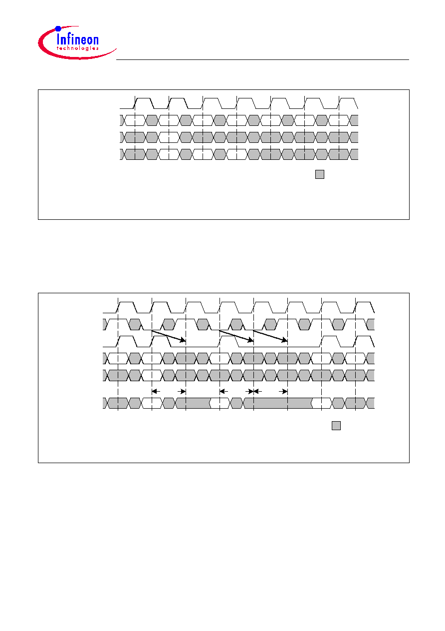
Consecutive READ Bursts . . . . . . . . . . . . . . . . . . . . . . . . . . . . . . . . . . . . . . . . . . . . . . . . . . . . . . . 22
Figure 16
Random READ Bursts . . . . . . . . . . . . . . . . . . . . . . . . . . . . . . . . . . . . . . . . . . . . . . . . . . . . . . . . . . 23
Figure 17
Non-Consecutive READ Bursts . . . . . . . . . . . . . . . . . . . . . . . . . . . . . . . . . . . . . . . . . . . . . . . . . . . 23
Figure 18
Terminating a READ Burst . . . . . . . . . . . . . . . . . . . . . . . . . . . . . . . . . . . . . . . . . . . . . . . . . . . . . . . 24
Figure 19
Clock Suspend Mode for READ Bursts . . . . . . . . . . . . . . . . . . . . . . . . . . . . . . . . . . . . . . . . . . . . . 24
Figure 20
READ Burst - DQM Operation . . . . . . . . . . . . . . . . . . . . . . . . . . . . . . . . . . . . . . . . . . . . . . . . . . . . 25
Figure 21
READ to WRITE Timing . . . . . . . . . . . . . . . . . . . . . . . . . . . . . . . . . . . . . . . . . . . . . . . . . . . . . . . . . 25
Figure 22
READ to PRECHARGE Timing . . . . . . . . . . . . . . . . . . . . . . . . . . . . . . . . . . . . . . . . . . . . . . . . . . . 26
Figure 23
WRITE Command. . . . . . . . . . . . . . . . . . . . . . . . . . . . . . . . . . . . . . . . . . . . . . . . . . . . . . . . . . . . . . 27
Figure 24
Basic WRITE Timing Parameters for DQs . . . . . . . . . . . . . . . . . . . . . . . . . . . . . . . . . . . . . . . . . . . 27
Figure 25
WRITE Burst (CAS Latency = 2) . . . . . . . . . . . . . . . . . . . . . . . . . . . . . . . . . . . . . . . . . . . . . . . . . . 28
Figure 26
WRITE Burst (CAS Latency = 3) . . . . . . . . . . . . . . . . . . . . . . . . . . . . . . . . . . . . . . . . . . . . . . . . . . 29
Figure 27
Consecutive WRITE Bursts . . . . . . . . . . . . . . . . . . . . . . . . . . . . . . . . . . . . . . . . . . . . . . . . . . . . . . 29
Figure 28
Random WRITE Bursts . . . . . . . . . . . . . . . . . . . . . . . . . . . . . . . . . . . . . . . . . . . . . . . . . . . . . . . . . 30
Figure 29
Non-Consecutive WRITE Bursts . . . . . . . . . . . . . . . . . . . . . . . . . . . . . . . . . . . . . . . . . . . . . . . . . . 30
Figure 30
Terminating a WRITE Burst . . . . . . . . . . . . . . . . . . . . . . . . . . . . . . . . . . . . . . . . . . . . . . . . . . . . . . 31
Figure 31
Clock Suspend Mode for WRITE Bursts. . . . . . . . . . . . . . . . . . . . . . . . . . . . . . . . . . . . . . . . . . . . . 31
Figure 32
WRITE Burst - DQM Operation . . . . . . . . . . . . . . . . . . . . . . . . . . . . . . . . . . . . . . . . . . . . . . . . . . . 32
Figure 33
WRITE to READ Timing . . . . . . . . . . . . . . . . . . . . . . . . . . . . . . . . . . . . . . . . . . . . . . . . . . . . . . . . . 32
Figure 34
WRITE to PRECHARGE Timing. . . . . . . . . . . . . . . . . . . . . . . . . . . . . . . . . . . . . . . . . . . . . . . . . . . 33
Figure 35
BURST TERMINATE Command . . . . . . . . . . . . . . . . . . . . . . . . . . . . . . . . . . . . . . . . . . . . . . . . . . 33
Figure 36
PRECHARGE Command . . . . . . . . . . . . . . . . . . . . . . . . . . . . . . . . . . . . . . . . . . . . . . . . . . . . . . . . 34
Figure 37
READ with Auto Precharge Interrupted by READ . . . . . . . . . . . . . . . . . . . . . . . . . . . . . . . . . . . . . 35
Figure 38
READ with Auto Precharge Interrupted by WRITE. . . . . . . . . . . . . . . . . . . . . . . . . . . . . . . . . . . . . 35
Figure 39
WRITE with Auto Precharge Interrupted by READ. . . . . . . . . . . . . . . . . . . . . . . . . . . . . . . . . . . . . 36
Figure 40
WRITE with Auto Precharge Interrupted by WRITE . . . . . . . . . . . . . . . . . . . . . . . . . . . . . . . . . . . . 36
Figure 41
AUTO REFRESH Command . . . . . . . . . . . . . . . . . . . . . . . . . . . . . . . . . . . . . . . . . . . . . . . . . . . . . 37
Figure 42
Auto Refresh. . . . . . . . . . . . . . . . . . . . . . . . . . . . . . . . . . . . . . . . . . . . . . . . . . . . . . . . . . . . . . . . . . 37
Figure 43
SELF REFRESH Entry Command . . . . . . . . . . . . . . . . . . . . . . . . . . . . . . . . . . . . . . . . . . . . . . . . . 38
Figure 44
Self Refresh Entry and Exit. . . . . . . . . . . . . . . . . . . . . . . . . . . . . . . . . . . . . . . . . . . . . . . . . . . . . . . 38
Figure 45
Power Down Entry Command . . . . . . . . . . . . . . . . . . . . . . . . . . . . . . . . . . . . . . . . . . . . . . . . . . . . 39
Figure 46
Power Down Entry and Exit . . . . . . . . . . . . . . . . . . . . . . . . . . . . . . . . . . . . . . . . . . . . . . . . . . . . . . 39
Figure 47
P-VFBGA-54-2
(Plastic Very Thin Fine Ball Grid Array Package)
. . . . . . . . . . . . . . . . . . . . . . . . . 49
List of Figures

HY[B/E]18L256160B[C/F]L-7.5
256-Mbit Mobile-RAM
Overview
Data Sheet
6
Rev. 1.72, 2005-07
01302004-CZ2R-J9SE
1
Overview
1.1
Features
∑
4 banks
◊
4 Mbit
◊
16 organization
∑
Fully synchronous to positive clock edge
∑
Four internal banks for concurrent operation
∑
Programmable CAS latency: 2, 3
∑
Programmable burst length: 1, 2, 4, 8 or full page
∑
Programmable wrap sequence: sequential or interleaved
∑
Programmable drive strength
∑
Auto refresh and self refresh modes
∑
8192 refresh cycles / 64 ms
∑
Auto precharge
∑
Commercial (0∞C to +70∞C) and Extended (-25
o
C to +85
o
C) operating temperature range
∑
54-ball P-VFBGA package (12.0
◊
8.0
◊
1.0 mm)
Power Saving Features
∑
Low supply voltages:
V
DD
= 1.65V to 1.95V,
V
DDQ
= 1.65V to 1.95V
∑
Optimized self refresh (
I
DD6
) and standby currents (
I
DD2
/
I
DD3
)
∑
Programmable Partial Array Self Refresh (PASR)
∑
Temperature Compensated Self-Refresh (TCSR), controlled by on-chip temperature sensor
∑
Power-Down and Deep Power Down modes
Table 1
Performance
Part Number Speed Code
- 7.5
Unit
Speed Grade
133
MHz
Access Time (
t
ACmax
)
CL = 3
5.4
ns
CL = 2
6.0
ns
Clock Cycle Time (
t
CKmin
)
CL = 3
7.5
ns
CL = 2
9.5
ns
Table 2
Memory Addressing Scheme
Item
Addresses
Banks
BA0, BA1
Rows
A0 - A12
Columns
A0 - A8
Data Sheet
7
Rev. 1.72, 2005-07
01302004-CZ2R-J9SE
HY[B/E]18L256160B[C/F]L-7.5
256-Mbit Mobile-RAM
Overview
1.2
Pin Configuration
Figure 1
Standard Ballout 256-Mbit Mobile-RAM
Table 3
Ordering Information
Type
1)
Description
Package
Commercial Temperature Range
HYB18L256160BC
133 MHz 4 Banks
◊
4 Mbit
◊
16 LP-SDRAM
P-VFBGA-54-2
HYB18L256160BF
133 MHz 4 Banks
◊
4 Mbit
◊
16 LP-SDRAM
P-VFBGA-54-2
Extended Temperature Range
HYE18L256160BC-7.5
133 MHz 4 Banks
◊
4 Mbit
◊
16 LP-SDRAM
P-VFBGA-54-2
HYE18L256160BCL-7.5 133 MHz 4 Banks
◊
4 Mbit
◊
16 LP-SDRAM
P-VFBGA-54-2
HYE18L256160BF-7.5
133 MHz 4 Banks
◊
4 Mbit
◊
16 LP-SDRAM
P-VFBGA-54-2
HYE18L256160BFL-7.5 133 MHz 4 Banks
◊
4 Mbit
◊
16 LP-SDRAM
1) HYB / HYE: Designator for memory products (HYB: standard temp. range; HYE: extended temp. range)
18L: 1.8V Mobile-RAM
256: 256 MBit density
160: 16 bit interface width
B: die revision
C / F: lead-containing product (C) / green product (F)
L: low-power product
-7.5: speed grade(s): min. clock cycle time
HY[B/E]18L256160B[C/F]L-7.5
256-Mbit Mobile-RAM
Overview
Data Sheet
8
Rev. 1.72, 2005-07
01302004-CZ2R-J9SE
1.3
Description
The HY[B/E]18L256160B[C/F]L is a high-speed CMOS, dynamic random-access memory containing 268,435,456
bits. It is internally configured as a quad-bank DRAM.
The HY[B/E]18L256160B[C/F]L achieves high speed data transfer rates by employing a chip architecture that
prefetches multiple bits and then synchronizes the output data to the system clock. Read and write accesses are
burst-oriented; accesses start at a selected location and continue for a programmed number of locations (1, 2, 4,
8 or full page) in a programmed sequence.
The device operation is fully synchronous: all inputs are registered at the positive edge of CLK.
The HY[B/E]18L256160B[C/F]L is especially designed for mobile applications. It operates from a 1.8V power
supply. Power consumption in self refresh mode is drastically reduced by an On-Chip Temperature Sensor
(OCTS); it can further be reduced by using the programmable Partial Array Self Refresh (PASR).
A conventional data-retaining Power-Down (PD) mode is available as well as a non-data-retaining Deep Power-
Down (DPD) mode.
The HY[B/E]18L256160B[C/F]L is housed in a 54-ball P-VFBGA package. It is available in Commercial (0
∞
C to
70
∞
C) and Extended (-25
∞
C to +85
∞
C) temperature range.
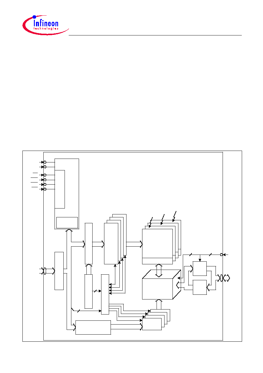
Figure 2
Functional Block Diagram
Data Sheet
9
Rev. 1.72, 2005-07
01302004-CZ2R-J9SE
HY[B/E]18L256160B[C/F]L-7.5
256-Mbit Mobile-RAM
Overview
1.4
Pin Definition and Description
Table 4
Pin Description
Ball
Type
Detailed Function
CLK
Input
Clock: all inputs are sampled on the positive edge of CLK.
CKE
Input
Clock Enable: CKE HIGH activates and CKE LOW deactivates internal clock signals,
device input buffers and output drivers. Taking CKE LOW provides PRECHARGE
POWER-DOWN and SELF REFRESH operation (all banks idle), ACTIVE POWER-
DOWN (row active in any bank) or SUSPEND (access in progress). Input buffers,
excluding CLK and CKE are disabled during power-down. Input buffers, excluding CKE
are disabled during SELF REFRESH.
CS
Input
Chip Select: All commands are masked when CS is registered HIGH. CS provides for
external bank selection on systems with multiple memory banks. CS is considered part of
the command code.
RAS, CAS,
WE
Input
Command Inputs: RAS, CAS and WE (along with CS) define the command being
entered.
DQ0 - DQ15 I/O
Data Inputs/Output: Bi-directional data bus (16 bit)
LDQM,
UDQM
Input
Input/Output Mask: input mask signal for WRITE cycles and output enable for READ
cycles. For WRITEs, DQM acts as a data mask when HIGH. For READs, DQM acts as
an output enable and places the output buffers in High-Z state when HIGH (two clocks
latency).
LDQM corresponds to the data on DQ0 - DQ7; UDQM to the data on DQ8 - DQ15.
BA0, BA1
Input
Bank Address Inputs: BA0 and BA1 define to which bank an ACTIVATE, READ, WRITE
or PRECHARGE command is being applied. BA0, BA1 also determine which mode
register is to be loaded during a MODE REGISTER SET command (MRS or EMRS).
A0 - A12
Input
Address Inputs: A0 - A12 define the row address during an ACTIVE command cycle. A0
- A8 define the column address during a READ or WRITE command cycle. In addition,
A10 (= AP) controls Auto Precharge operation at the end of the burst read or write cycle.
During a PRECHARGE command, A10 (= AP) in conjunction with BA0, BA1 controls
which bank(s) are to be precharged: if A10 is HIGH, all four banks will be precharged
regardless of the state of BA0 and BA1; if A10 is LOW, BA0, BA1 define the bank to be
precharged. During MODE REGISTER SET commands, the address inputs hold the op-
code to be loaded.
V
DDQ
Supply I/O Power Supply: Isolated power for DQ output buffers for improved noise immunity:
V
DDQ
= 1.65V to 1.95V
V
SSQ
Supply I/O Ground
V
DD
Supply Power Supply: Power for the core logic and input buffers,
V
DD
= 1.65V to 1.95V
V
SS
Supply Ground
N.C.
≠
No Connect
HY[B/E]18L256160B[C/F]L-7.5
256-Mbit Mobile-RAM
Functional Description
Data Sheet
10
Rev. 1.72, 2005-07
01302004-CZ2R-J9SE
2
Functional Description
The 256-Mbit Mobile-RAM is a high-speed CMOS, dynamic random-access memory containing 268,435,456 bits.
It is internally configured as a quad-bank DRAM.
READ and WRITE accesses to the Mobile-RAM are burst oriented; accesses start at a selected location and
continue for a programmed number of locations in a programmed sequence. Accesses begin with the registration
of an ACTIVE command, followed by a READ or WRITE command. The address bits registered coincident with
the ACTIVE command are used to select the bank and row to be accessed (BA0, BA1 select the banks, A0 - A12
select the row). The address bits registered coincident with the READ or WRITE command are used to select the
starting column location for the burst access.
Prior to normal operation, the Mobile-RAM must be initialized. The following sections provide detailed information
covering device initialization, register definition, command description and device operation.
2.1
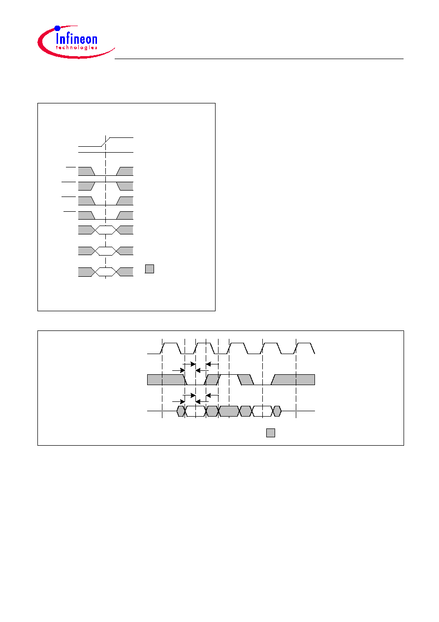
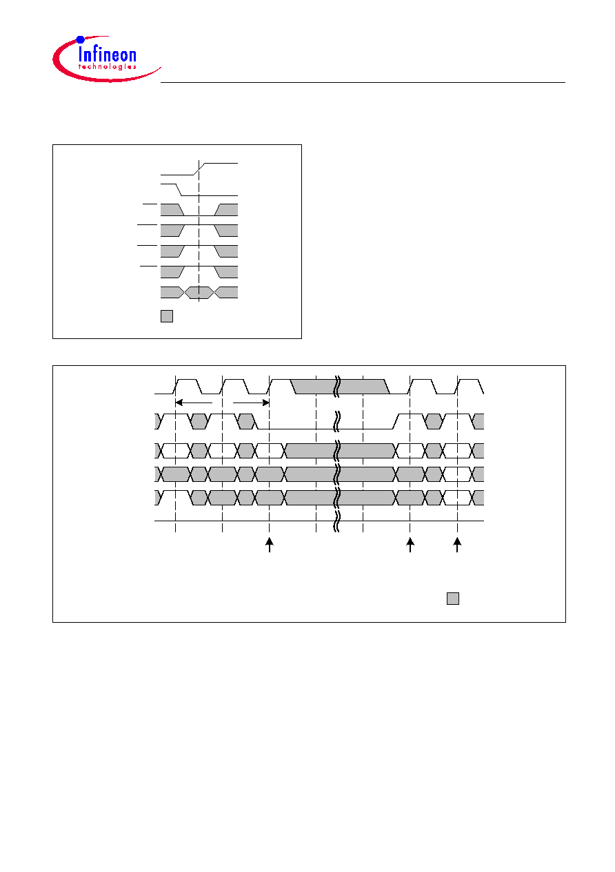
Power On and Initialization
The Mobile-RAM must be powered up and initialized in a predefined manner (see
Figure 3
). Operational
procedures other than those specified may result in undefined operation.
Figure 3
Power-Up Sequence and Mode Register Sets
Data Sheet
11
Rev. 1.72, 2005-07
01302004-CZ2R-J9SE
HY[B/E]18L256160B[C/F]L-7.5
256-Mbit Mobile-RAM
Functional Description
1. At first, device core power (V
DD
) and device IO power (V
DDQ
) must be brought up simultaneously. Typically V
DD
and V
DDQ
are driven from a single power converter output.
Assert and hold CKE and DQM to a HIGH level.
2. After V
DD
and V
DDQ
are stable and CKE is HIGH, apply stable clocks.
3. Wait for 200µs while issuing NOP or DESELECT commands.
4. Issue a PRECHARGE ALL command, followed by NOP or DESELECT commands for at least t
RP
period.
5. Issue two AUTO REFRESH commands, each followed by NOP or DESELECT commands for at least t
RC
period.
6. Issue two MODE REGISTER SET commands for programming the Mode Register and Extended Mode
Register, each followed by NOP or DESELECT commands for at least t
MRD
period; the order in which both
registers are programmed is not important. Programming of the Extended Mode Register may be omitted when
default values (half drive strength, 4 bank refresh) will be used.
Following these steps, the Mobile-RAM is ready for normal operation.
2.2
Register Definition
2.2.1
Mode Register
The Mode Register is used to define the specific mode of operation of the Mobile-RAM. This definition includes
the selection of a burst length (bits A0-A2), a burst type (bit A3), a CAS latency (bits A4-A6), and a write burst
mode (bit A9). The Mode Register is programmed via the MODE REGISTER SET command (with BA0 = 0 and
BA1 = 0) and will retain the stored information until it is programmed again or the device loses power.
The Mode Register must be loaded when all banks are idle, and the controller must wait the specified time before
initiating any subsequent operation. Violating either of these requirements results in unspecified operation.
Reserved states should not be used, as unknown operation or incompatibility with future versions may result.
MR
Mode Register Definition
(BA[1:0] = 00
B
)
BA1
BA0
A12
A11
A10
A9
A8
A7
A6
A5
A4
A3
A2
A1
A0
0
0
0
0
0
WB
0
0
CL
BT
BL
Field
Bits
Type Description
WB
9
w
Write Burst Mode
0
Burst Write
1
Single Write
CL
[6:4]
w
CAS Latency
010 2
011 3
Note: All other bit combinations are RESERVED.
BT
3
w
Burst Type
0
Sequential
1
Interleaved
HY[B/E]18L256160B[C/F]L-7.5
256-Mbit Mobile-RAM
Functional Description
Data Sheet
12
Rev. 1.72, 2005-07
01302004-CZ2R-J9SE
2.2.1.1
Burst Length
READ and WRITE accesses to the Mobile-RAM are burst oriented, with the burst length being programmable. The
burst length determines the maximum number of column locations that can be accessed for a given READ or
WRITE command. Burst lengths of 1, 2, 4, 8 locations are available for both the sequential and interleaved burst
types, and a full-page burst mode is available for the sequential burst type.
When a READ or WRITE command is issued, a block of columns equal to the burst length is effectively selected.
All accesses for that burst take place within this block, meaning that the burst wraps within the block if a boundary
is reached. The block is uniquely selected by A1-A8 when the burst length is set to two, by A2-A8 when the burst
length is set to four and by A3-A8 when the burst length is set to eight. The remaining (least significant) address
bit(s) is (are) used to select the starting location within the block.
Full page bursts wrap within the page if the boundary is reached. Please note that full page bursts do not self-
terminate; this implies that full-page read or write bursts with Auto Precharge are not legal commands.
Notes
1. For a burst length of 2, A1-Ai select the two-data-element block; A0 selects the first access within the block.
2. For a burst length of 4, A2-Ai select the four-data-element block; A0-A1 select the first access within the block.
3. For a burst length of 8, A3-Ai select the eight-data-element block; A0-A2 select the first access within the block.
4. For a full page burst, A0-Ai select the starting data element.
BL
[2:0]
w
Burst Length
000 1
001 2
010 4
011 8
111 full page (Sequential burst type only)
Note: All other bit combinations are RESERVED.
Table 5
Burst Definition
Burst Length
Starting Column Address
Order of Accesses Within a Burst
A2
A1
A0
Sequential
Interleaved
2
0
0 - 1
0 - 1
1
1 - 0
1 - 0
4
0
0
0 - 1 - 2 - 3
0 - 1 - 2 - 3
0
1
1 - 2 - 3 - 0
1 - 0 - 3 - 2
1
0
2 - 3 - 0 - 1
2 - 3 - 0 - 1
1
1
3 - 0 - 1 - 2
3 - 2 - 1 - 0
8
0
0
0
0 - 1 - 2 - 3 - 4 - 5 - 6 - 7
0 - 1 - 2 - 3 - 4 - 5 - 6 - 7
0
0
1
1 - 2 - 3 - 4 - 5 - 6 - 7 - 0
1 - 0 - 3 - 2 - 5 - 4 - 7 - 6
0
1
0
2 - 3 - 4 - 5 - 6 - 7 - 0 - 1
2 - 3 - 0 - 1 - 6 - 7 - 4 - 5
0
1
1
3 - 4 - 5 - 6 - 7 - 0 - 1 - 2
3 - 2 - 1 - 0 - 7 - 6 - 5 - 4
1
0
0
4 - 5 - 6 - 7 - 0 - 1 - 2 - 3
4 - 5 - 6 - 7 - 0 - 1 - 2 - 3
1
0
1
5 - 6 - 7 - 0 - 1 - 2 - 3 - 4
5 - 4 - 7 - 6 - 1 - 0 - 3 - 2
1
1
0
6 - 7 - 0 - 1 - 2 - 3 - 4 - 5
6 - 7 - 4 - 5 - 2 - 3 - 0 - 1
1
1
1
7 - 0 - 1 - 2 - 3 - 4 - 5 - 6
7 - 6 - 5 - 4 - 3 - 2 - 1 - 0
Full Page
n
n
n
Cn, Cn+1, Cn+2, ...
not supported
Field
Bits
Type Description
Data Sheet
13
Rev. 1.72, 2005-07
01302004-CZ2R-J9SE
HY[B/E]18L256160B[C/F]L-7.5
256-Mbit Mobile-RAM
Functional Description
5. Whenever a boundary of the block is reached within a given sequence, the following access wraps within the
block.
2.2.1.2
Burst Type
Accesses within a given burst may be programmed to be either sequential or interleaved; this is referred to as the
burst type and is selected via bit A3. The ordering of accesses within a burst is determined by the burst length, the
burst type and the starting column address, as shown in
Table 5
.
2.2.1.3
Read Latency
The Read latency, or CAS latency, is the delay, in clock cycles, between the registration of a READ command and
the availability of the first piece of output data. The latency can be programmed to 2 or 3 clocks.
If a READ command is registered at clock edge n, and the latency is m clocks, the data will be available with clock
edge n + m (for details please refer to the READ command description).
2.2.1.4
Write Burst Mode
When A9 = 0, the burst length programmed via A0-A2 applies to both read and write bursts; when A9 = 1, write
accesses consist of single data elements only.
2.2.1.5
Extended Mode Register
The Extended Mode Register controls additional low power features of the device. These include the Partial Array
Self Refresh (PASR, bits A0-A2)), the Temperature Compensated Self Refresh (TCSR, bits A3-A4)) and the drive
strength selection for the DQs (bits A5-A6). The Extended Mode Register is programmed via the MODE
REGISTER SET command (with BA0 = 0 and BA1 = 1) and will retain the stored information until it is programmed
again or the device loses power.
The Extended Mode Register must be loaded when all banks are idle, and the controller must wait the specified
time before initiating any subsequent operation. Violating either of these requirements result in unspecified
operation.
Reserved states should not be used, as unknown operation or incompatibility with future versions may result.
EMR
Extended Mode Register
(BA[1:0] = 10
B
)
BA1
BA0
A12
A11
A10
A9
A8
A7
A6
A5
A4
A3
A2
A1
A0
1
0
0
0
0
0
0
0
DS
(TCSR)
PASR
Field
Bits
Type Description
DS
[6:5]
w
Selectable Drive Strength
00
Full Drive Strength
01
Half Drive Strength (default)
Note: All other bit combinations are RESERVED.
TCSR [4:3]
w
Temperature Compensated Self Refresh
XX
Superseded by on-chip temperature sensor (see text)

HY[B/E]18L256160B[C/F]L-7.5
256-Mbit Mobile-RAM
Functional Description
Data Sheet
14
Rev. 1.72, 2005-07
01302004-CZ2R-J9SE
2.2.1.6
Partial Array Self Refresh (PASR)
Partial Array Self Refresh is a power-saving feature specific to Mobile RAMs. With PASR, self refresh may be
restricted to variable portions of the total array. The selection comprises all four banks, two banks, one bank, half
of one bank, and a quarter of one bank. Data written to the non activated memory sections will get lost after a
period defined by
t
REF
(cf.
Table 13
).
2.2.1.7
Temperature Compensated Self Refresh (TCSR) with On-Chip Temperature
Sensor
DRAM devices store data as electrical charge in tiny capacitors that require a periodic refresh in order to retain
the stored information. This refresh requirement heavily depends on the die temperature: high temperatures
correspond to short refresh periods, and low temperatures correspond to long refresh periods.
The Mobile-RAM is equipped with an on-chip temperature sensor which continuously senses the actual die
temperature and adjusts the refresh period in Self Refresh mode accordingly. This makes any programming of the
TCSR bits in the Extended Mode Register obsolete. It also is the superior solution in terms of compatibility and
power-saving, because
∑
it is fully compatible to all processors that do not support the Extended Mode Register
∑
it is fully compatible to all applications that only write a default (worst case) TCSR value, e.g. because of the
lack of an external temperature sensor
∑
it does not require any processor interaction for regular TCSR updates
2.2.1.8
Selectable Drive Strength
The drive strength of the DQ output buffers is selectable via bits A5 and A6 and shall be set load dependent. The
half drive strength is suitable for typical Mobile-RAM applications. The full drive strength is intended for heavier
loaded systems.
I
-
V
curves for full drive strength and half drive strength can be found in
Table 23
.
PASR [2:0]
w
Partial Array Self Refresh
000 all banks (default)
001 1/2 array (BA1 = 0)
010 1/4 array (BA1 = BA0 = 0)
101 1/8 array (BA1 = BA0 = RA12 = 0)
110 1/16 array (BA1 = BA0 = RA12 = RA11 = 0)
Note: All other bit combinations are RESERVED.
Field
Bits
Type Description
Data Sheet
15
Rev. 1.72, 2005-07
01302004-CZ2R-J9SE
HY[B/E]18L256160B[C/F]L-7.5
256-Mbit Mobile-RAM
Functional Description
2.3
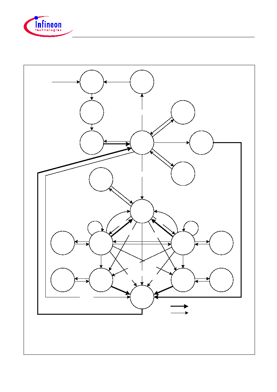
State Diagram
Figure 4
State Diagram
HY[B/E]18L256160B[C/F]L-7.5
256-Mbit Mobile-RAM
Functional Description
Data Sheet
16
Rev. 1.72, 2005-07
01302004-CZ2R-J9SE
2.4
Commands
Address (A0 - A12, BA0, BA1), write data (DQ0 - DQ15) and command inputs (CKE, CS, RAS, CAS, WE, DQM)
are all registered on the positive edge of CLK.
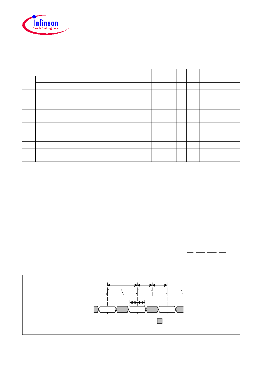
Figure 5
shows the basic timing parameters, which apply to all
commands and operations.
Figure 5
Address / Command Inputs Timing Parameters
Table 6
Command Overview
Command
CS RAS CAS WE DQM
Address
Notes
NOP
DESELECT
H
X
X
X
X
X
1)
1) DESELECT and NOP are functionally interchangeable.
NO OPERATION
L
H
H
H
X
X
1)
ACT
ACTIVE (Select bank and row)
L
L
H
H
X
Bank / Row
2)
2) BA0, BA1 provide bank address, and A0 - A12 provide row address.
RD
READ (Select bank and column and start read burst)
L
H
L
H
L/H
Bank / Col
3)
3) BA0, BA1 provide bank address, A0 - A8 provide column address; A10 HIGH enables the Auto Precharge feature (non
persistent), A10 LOW disables the Auto Precharge feature.
WR
WRITE (Select bank and column and start write burst) L
H
L
L
L/H
Bank / Col
3)
BST
BURST TERMINATE or
DEEP POWER DOWN
L
H
H
L
X
X
4)
4) This command is BURST TERMINATE if CKE is HIGH, DEEP POWER DOWN if CKE is LOW. The BURST TERMINATE
command is defined for READ or WRITE bursts with Auto Precharge disabled only.
PRE
PRECHARGE (Deactivate row in bank or banks)
L
L
H
L
X
Code
5)
5) A10 LOW: BA0, BA1 determine which bank is precharged.
A10 HIGH: all banks are precharged and BA0, BA1 are "Don't Care".
ARF
AUTO REFRESH or
SELF REFRESH (enter self refresh mode)
L
L
L
H
X
X
6)7)
6) This command is AUTO REFRESH if CKE is HIGH, SELF REFRESH if CKE is LOW.
7) Internal refresh counter controls row and bank addressing; all inputs and I/Os are "Don't Care" except for CKE.
MRS MODE REGISTER SET
L
L
L
L
X
Op-Code
8)
8) BA0, BA1 select either the Mode Register (BA0 = 0, BA1 = 0) or the Extended Mode Register (BA0 = 0, BA1 = 1); other
combinations of BA0, BA1 are reserved; A0 - A12 provide the op-code to be written to the selected mode register.
≠
Data Write / Output Enable
≠
≠
≠
≠
L
≠
9)
9) DQM LOW: data present on DQs is written to memory during write cycles; DQ output buffers are enabled during read
cycles;
DQM HIGH: data present on DQs are masked and thus not written to memory during write cycles; DQ output buffers are
placed in High-Z state (two clocks latency) during read cycles.
≠
Write Mask / Output Disable (High-Z)
≠
≠
≠
≠
H
≠
9)
Data Sheet
17
Rev. 1.72, 2005-07
01302004-CZ2R-J9SE
HY[B/E]18L256160B[C/F]L-7.5
256-Mbit Mobile-RAM
Functional Description
2.4.1
NO OPERATION (NOP)
Figure 6
No Operation Command
The NO OPERATION (NOP) command is used to
perform a NOP to a Mobile-RAM which is selected (CS
= LOW). This prevents unwanted commands from
being registered during idle states. Operations already
in progress are not affected.
2.4.2
DESELECT
The DESELECT function (CS = HIGH) prevents new commands from being executed by the Mobile-RAM. The
Mobile-RAM is effectively deselected. Operations already in progress are not affected.
Table 7
Inputs Timing Parameters
Parameter
Symbol
- 7.5
Unit
Notes
min.
max.
Clock cycle time
CL = 3
t
CK
7.5
--
ns
--
CL = 2
9.5
--
ns
Clock frequency
CL = 3
f
CK
--
133
MHz
--
CL = 2
--
105
MHz
Clock high-level width
t
CH
2.5
--
ns
--
Clock low-level width
t
CL
2.5
--
ns
--
Address and command input setup time
t
IS
1.5
--
ns
--
Address and command input hold time
t
IH
0.5
--
ns
--
HY[B/E]18L256160B[C/F]L-7.5
256-Mbit Mobile-RAM
Functional Description
Data Sheet
18
Rev. 1.72, 2005-07
01302004-CZ2R-J9SE
2.4.3
MODE REGISTER SET
Figure 7
Mode Register Set Command
The Mode Register and Extended Mode Register are
loaded via inputs A0 - A12 (see mode register
descriptions in
Chapter 2.2
). The MODE REGISTER
SET command can only be issued when all banks are
idle and no bursts are in progress. A subsequent
executable command cannot be issued until
t
MRD
is
met.
Figure 8
Mode Register Definition
Table 8
Timing Parameters for Mode Register Set Command
Parameter
Symbol
- 7.5
Units
Notes
min.
max.
MODE REGISTER SET command period
t
MRD
2
≠
t
CK
≠
Data Sheet
19
Rev. 1.72, 2005-07
01302004-CZ2R-J9SE
HY[B/E]18L256160B[C/F]L-7.5
256-Mbit Mobile-RAM
Functional Description
2.4.4
ACTIVE
Figure 9
ACTIVE Command
Before any READ or WRITE commands can be issued
to a bank within the Mobile-RAM, a row in that bank
must be "opened" (activated). This is accomplished via
the ACTIVE command and addresses A0 - A12, BA0
and BA1 (see
Figure 9
), which decode and select both
the bank and the row to be activated. After opening a
row (issuing an ACTIVE command), a READ or WRITE
command may be issued to that row, subject to the
t
RCD
specification. A subsequent ACTIVE command to a
different row in the same bank can only be issued after
the previous active row has been "closed"
(precharged).
The minimum time interval between successive
ACTIVE commands to the same bank is defined by
t
RC
.
A subsequent ACTIVE command to another bank can
be issued while the first bank is being accessed, which
results in a reduction of total row-access overhead. The
minimum time interval between successive ACTIVE
commands to different banks is defined by
t
RRD
.
Figure 10
Bank Activate Timings
Table 9
Timing Parameters for ACTIVE Command
Parameter
Symbol
- 7.5
Units
Notes
min.
max.
ACTIVE to ACTIVE command period
t
RC
67
≠
ns
1)
1) These parameters account for the number of clock cycles and depend on the operating frequency as follows:
no. of clock cycles = specified delay / clock period; round up to next integer.
ACTIVE to READ or WRITE delay
t
RCD
19
≠
ns
1)
ACTIVE bank A to ACTIVE bank B delay
t
RRD
15
≠
ns
1)
HY[B/E]18L256160B[C/F]L-7.5
256-Mbit Mobile-RAM
Functional Description
Data Sheet
20
Rev. 1.72, 2005-07
01302004-CZ2R-J9SE
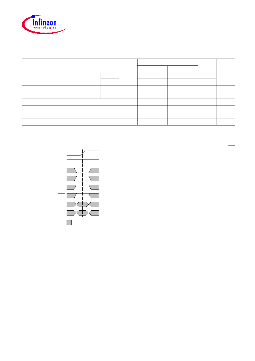
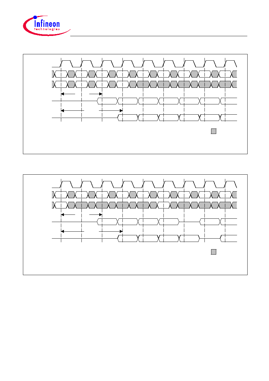
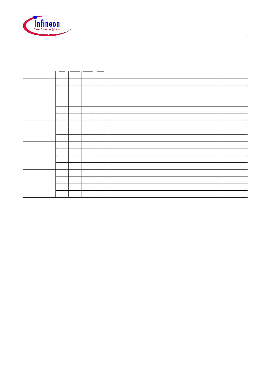
2.4.5
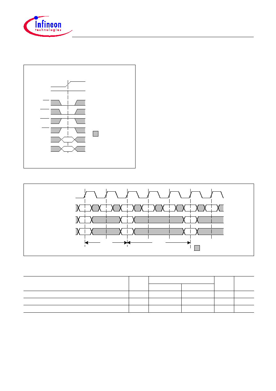
READ
Figure 11
READ Command
Subsequent to programming the mode register with
CAS latency and burst length, READ bursts are
initiated with a READ command, as shown in
Figure 11
. Basic timings for the DQs are shown in
Figure 12
; they apply to all read operations and
therefore are omitted from all subsequent timing
diagrams.
The starting column and bank addresses are provided
with the READ command and Auto Precharge is either
enabled or disabled for that burst access. If Auto
Precharge is enabled, the row being accessed starts
precharge at the completion of the burst, provided
t
RAS
has been satisfied. For the generic READ commands
used in the following illustrations, Auto Precharge is
disabled.
Figure 12
Basic READ Timing Parameters for DQs
Data Sheet
21
Rev. 1.72, 2005-07
01302004-CZ2R-J9SE
HY[B/E]18L256160B[C/F]L-7.5
256-Mbit Mobile-RAM
Functional Description
During READ bursts, the valid data-out element from the starting column address is available following the CAS
latency after the READ command. Each subsequent data-out element is valid nominally at the next positive clock
edge. Upon completion of a READ burst, assuming no other READ command has been initiated, the DQs go to
High-Z state.
Figure 13
and
Figure 14
show single READ bursts for each supported CAS latency setting.
Figure 13
Single READ Burst (CAS Latency = 2)
Table 10
Timing Parameters for READ
Parameter
Symbol
- 7.5
Units
Notes
min.
max.
Access time from CLK
CL = 3
t
AC
≠
5.4
ns
≠
CL = 2
t
AC
≠
6.0
ns
DQ low-impedance time from CLK
t
LZ
1.0
≠
ns
≠
DQ high-impedance time from CLK
t
HZ
3.0
7.0
ns
Data out hold time
t
OH
2.5
≠
ns
≠
DQM to DQ High-Z delay (READ Commands)
t
DQZ
≠
2
t
CK
≠
ACTIVE to ACTIVE command period
t
RC
67
≠
ns
1)
ACTIVE to READ or WRITE delay
t
RCD
19
≠
ns
1)
ACTIVE to PRECHARGE command period
t
RAS
45
100k
ns
1)
PRECHARGE command period
t
RP
19
≠
ns
1)
1) These parameters account for the number of clock cycles and depend on the operating frequency as follows:
no. of clock cycles = specified delay / clock period; round up to next integer.
HY[B/E]18L256160B[C/F]L-7.5
256-Mbit Mobile-RAM
Functional Description
Data Sheet
22
Rev. 1.72, 2005-07
01302004-CZ2R-J9SE
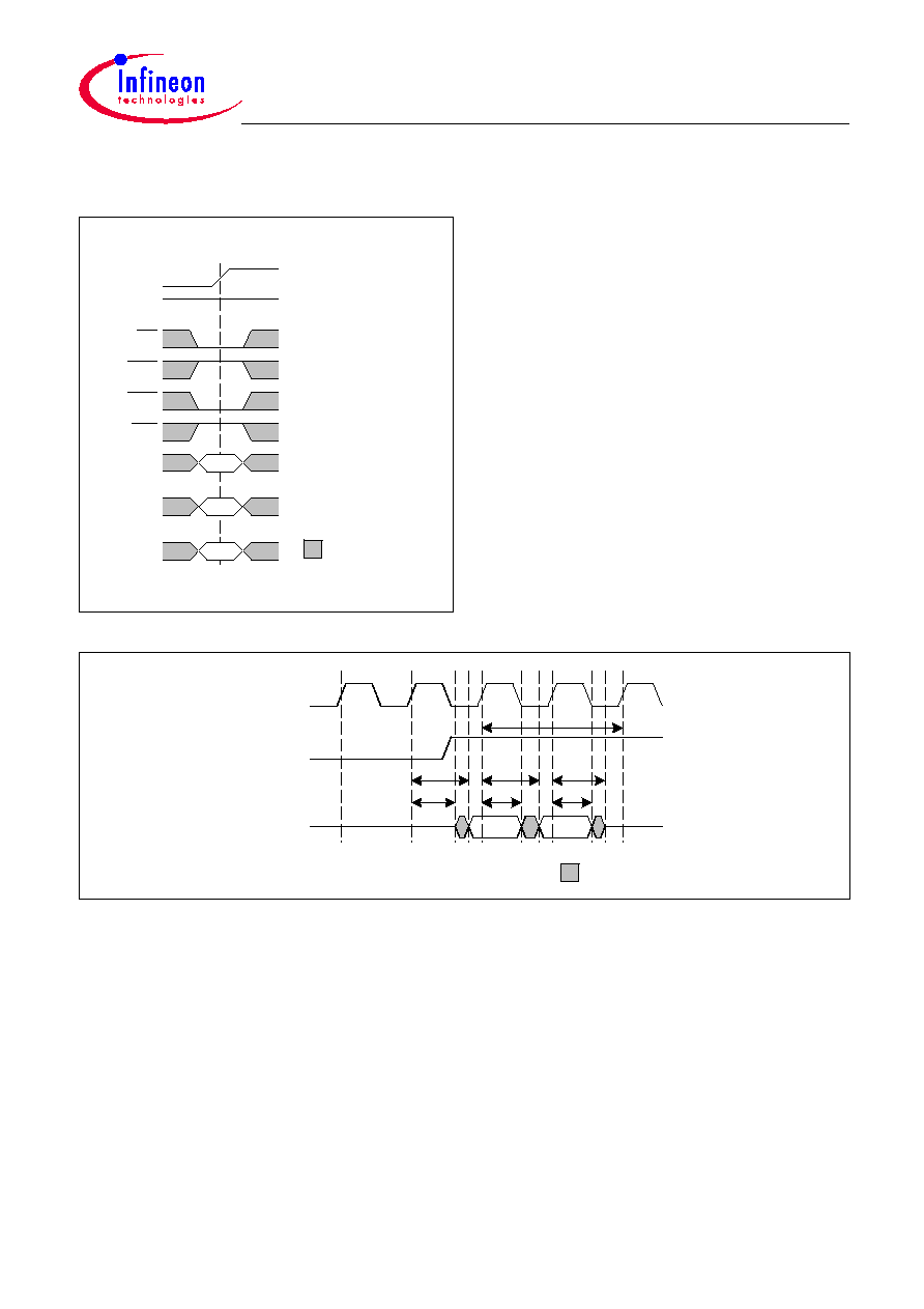
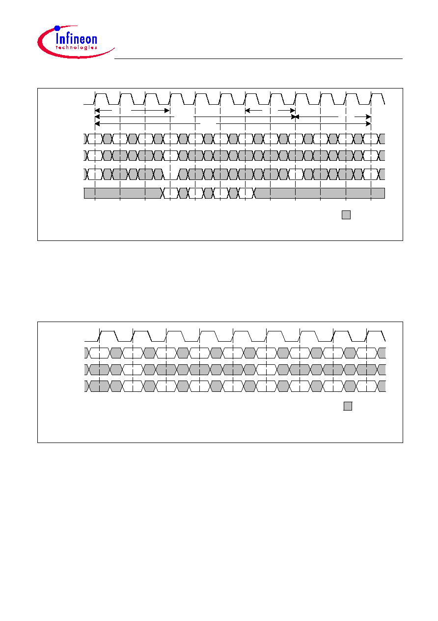
Figure 14
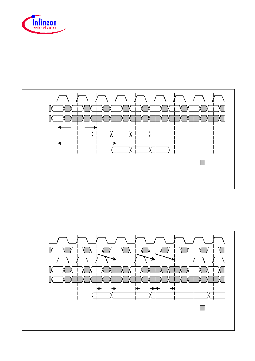
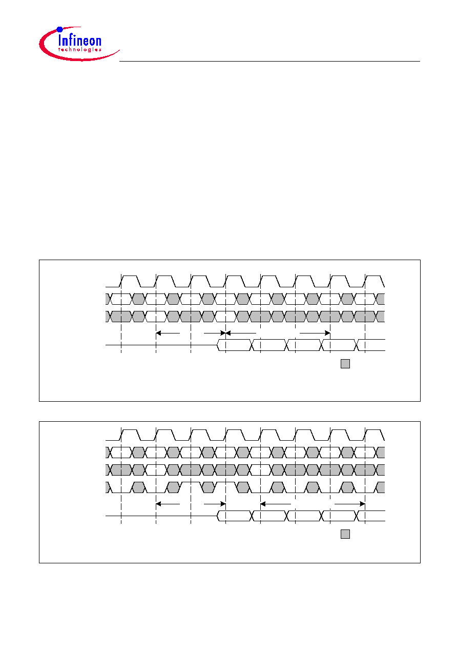
Single READ Burst (CAS Latency = 3)
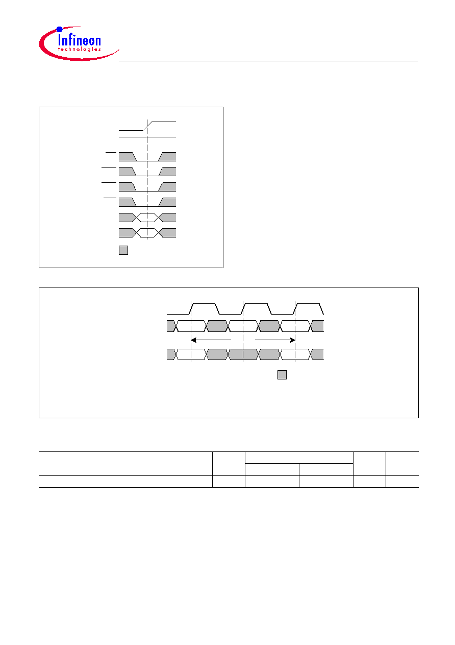
Data from any READ burst may be concatenated with data from a subsequent READ command. In either case, a
continuous flow of data can be maintained. A READ command can be initiated on any clock cycle following a
previous READ command, and may be performed to the same or a different (active) bank. The first data element
from the new burst follows either the last element of a completed burst (
Figure 15
) or the last desired data element
of a longer burst which is being truncated (
Figure 16
). The new READ command should be issued x cycles after
the first READ command, where x equals the number of desired data elements.
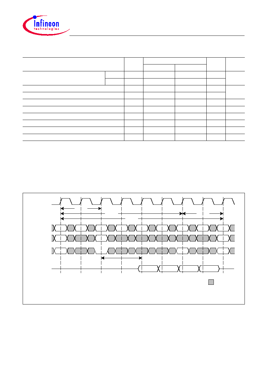
Figure 15
Consecutive READ Bursts
Data Sheet
23
Rev. 1.72, 2005-07
01302004-CZ2R-J9SE
HY[B/E]18L256160B[C/F]L-7.5
256-Mbit Mobile-RAM
Functional Description
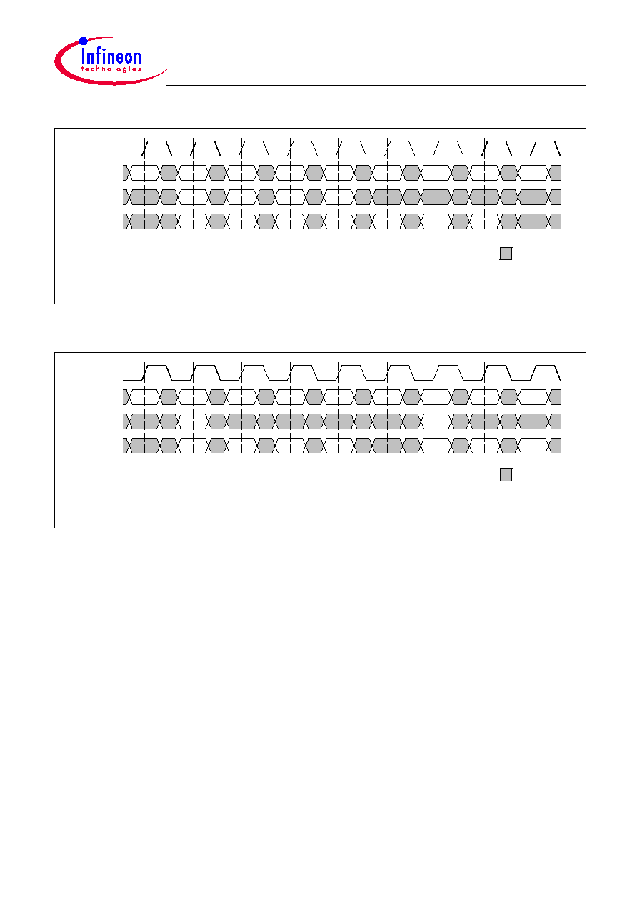
Figure 16
Random READ Bursts
Non-consecutive READ bursts are shown in
Figure 17
.
Figure 17
Non-Consecutive READ Bursts
HY[B/E]18L256160B[C/F]L-7.5
256-Mbit Mobile-RAM
Functional Description
Data Sheet
24
Rev. 1.72, 2005-07
01302004-CZ2R-J9SE
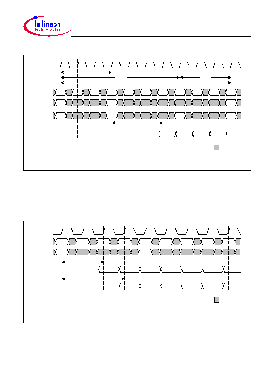
2.4.5.1
READ Burst Termination
Data from any READ burst may be truncated using the BURST TERMINATE command (see
Page 33
), provided
that Auto Precharge was not activated. The BURST TERMINATE latency is equal to the CAS latency, i.e. the
BURST TERMINATE command must be issued x clock cycles before the clock edge at which the last desired data
element is valid, where x equals the CAS latency for READ bursts minus 1. This is shown in
Figure 18
. The
BURST TERMINATE command may be used to terminate a full-page READ which does not self-terminate.
Figure 18
Terminating a READ Burst
2.4.5.2
Clock Suspend Mode for READ Cycles
Clock suspend mode allows to extend any read burst in progress by a variable number of clock cycles. As long as
CKE is registered LOW, the following internal clock pulse(s) will be ignored and data on DQ will remain driven, as
shown in
Figure 19
.
Figure 19
Clock Suspend Mode for READ Bursts
Data Sheet
25
Rev. 1.72, 2005-07
01302004-CZ2R-J9SE
HY[B/E]18L256160B[C/F]L-7.5
256-Mbit Mobile-RAM
Functional Description
2.4.5.3
READ - DQM Operation
DQM may be used to suppress read data and place the output buffers into High-Z state. The generic timing
parameters as listed in
Table 10
also apply to this DQM operation. The read burst in progress is not affected and
will continue as programmed.
Figure 20
READ Burst - DQM Operation
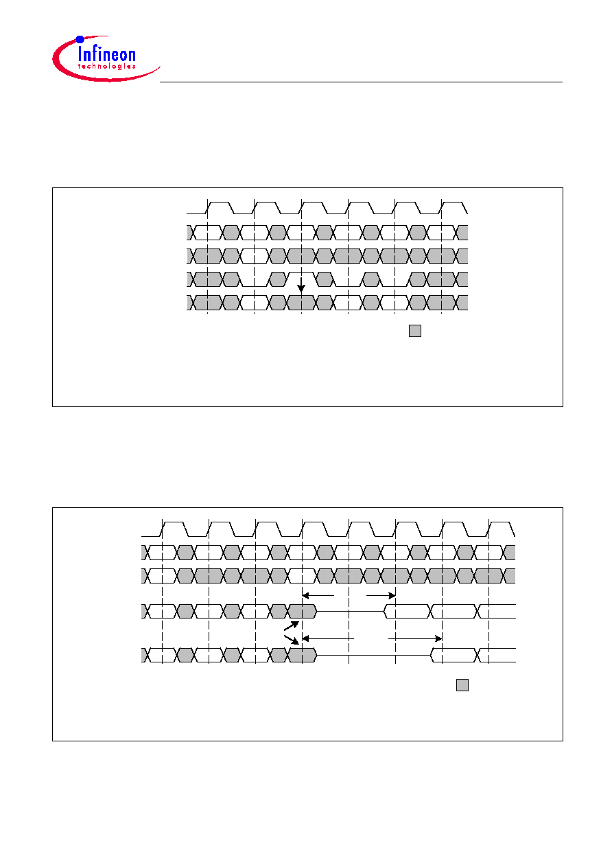
2.4.5.4
READ to WRITE
A READ burst may be followed by or truncated with a WRITE command. The WRITE command can be performed
to the same or a different (active) bank. Care must be taken to avoid bus contention on the DQs; therefore it is
recommended that the DQs are held in High-Z state for a minimum of 1 clock cycle. This can be achieved by either
delaying the WRITE command, or suppressing the data-out from the READ by pulling DQM HIGH two clock cycles
prior to the WRITE command, as shown in
Figure 21
. With the registration of the WRITE command, DQM acts as
a write mask: when asserted HIGH, input data will be masked and no write will be performed.
Figure 21
READ to WRITE Timing
HY[B/E]18L256160B[C/F]L-7.5
256-Mbit Mobile-RAM
Functional Description
Data Sheet
26
Rev. 1.72, 2005-07
01302004-CZ2R-J9SE
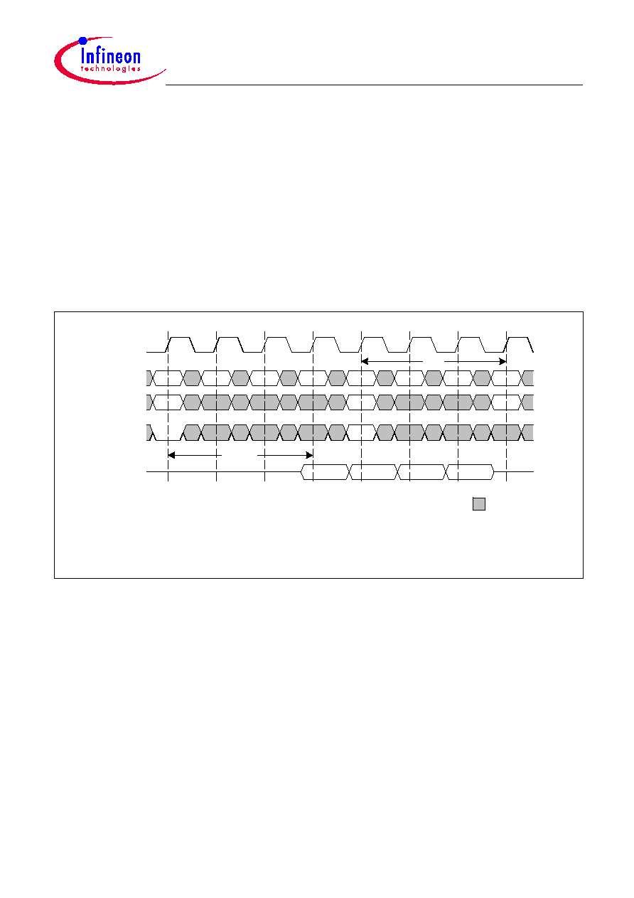
2.4.5.5
READ to PRECHARGE
A READ burst may be followed by, or truncated with a PRECHARGE command to the same bank, provided that
Auto Precharge was not activated. This is shown in
Figure 22
.
The PRECHARGE command should be issued x clock cycles before the clock edge at which the last desired data
element is valid, where x equals the CAS latency for READ bursts minus 1. Following the PRECHARGE
command, a subsequent ACTIVE command to the same bank cannot be issued until
t
RP
is met. Please note that
part of the row precharge time is hidden during the access of the last data elements.
In the case of a READ being executed to completion, a PRECHARGE command issued at the optimum time (as
described above) provides the same operation that would result from the same READ burst with Auto Precharge
enabled. The disadvantage of the PRECHARGE command is that it requires that the command and address
busses be available at the appropriate time to issue the command. The advantage of the PRECHARGE command
is that it can be used to truncate bursts.
Figure 22
READ to PRECHARGE Timing
Data Sheet
27
Rev. 1.72, 2005-07
01302004-CZ2R-J9SE
HY[B/E]18L256160B[C/F]L-7.5
256-Mbit Mobile-RAM
Functional Description
2.4.6
WRITE
Figure 23
WRITE Command
WRITE bursts are initiated with a WRITE command, as
shown in
Figure 23
. Basic timings for the DQs are
shown in
Figure 24
; they apply to all write operations.
The starting column and bank addresses are provided
with the WRITE command, and Auto Precharge is
either enabled or disabled for that access. If Auto
Precharge is enabled, the row being accessed is
precharged at the completion of the write burst. For the
generic WRITE commands used in the following
illustrations, Auto Precharge is disabled.
Figure 24
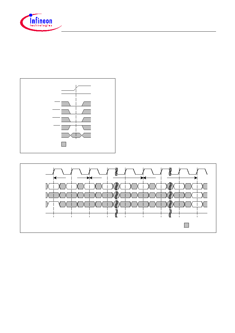
Basic WRITE Timing Parameters for DQs
During WRITE bursts, the first valid data-in element is registered coincident with the WRITE command, and
subsequent data elements are registered on each successive positive edge of CLK. Upon completion of a burst,
assuming no other commands have been initiated, the DQs remain in High-Z state, and any additional input data
is ignored.
Figure 25
and
Figure 26
show a single WRITE burst for each supported CAS latency setting.
HY[B/E]18L256160B[C/F]L-7.5
256-Mbit Mobile-RAM
Functional Description
Data Sheet
28
Rev. 1.72, 2005-07
01302004-CZ2R-J9SE
Figure 25
WRITE Burst (CAS Latency = 2)
Table 11
Timing Parameters for WRITE
Parameter
Symbol
- 7.5
Units
Notes
min.
max.
DQ and DQM input setup time
t
IS
1.5
--
ns
--
DQ input hold time
t
IH
0.8
--
ns
--
DQM input hold time
0.5
--
ns
--
DQM write mask latency
t
DQW
0
--
t
CK
--
ACTIVE to ACTIVE command period
t
RC
67
--
ns
1)
ACTIVE to READ or WRITE delay
t
RCD
19
--
ns
1)
ACTIVE to PRECHARGE command period
t
RAS
45
100k
ns
1)
WRITE recovery time
t
WR
14
--
ns
1)
PRECHARGE command period
t
RP
19
--
ns
1)
1) These parameters account for the number of clock cycles and depend on the operating frequency as follows:
no. of clock cycles = specified delay / clock period; round up to next integer.
Data Sheet
29
Rev. 1.72, 2005-07
01302004-CZ2R-J9SE
HY[B/E]18L256160B[C/F]L-7.5
256-Mbit Mobile-RAM
Functional Description
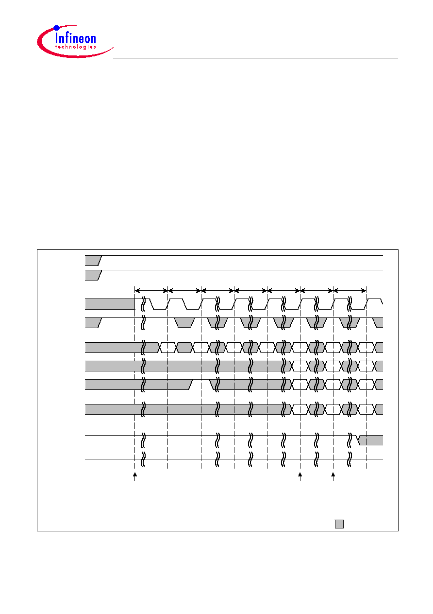
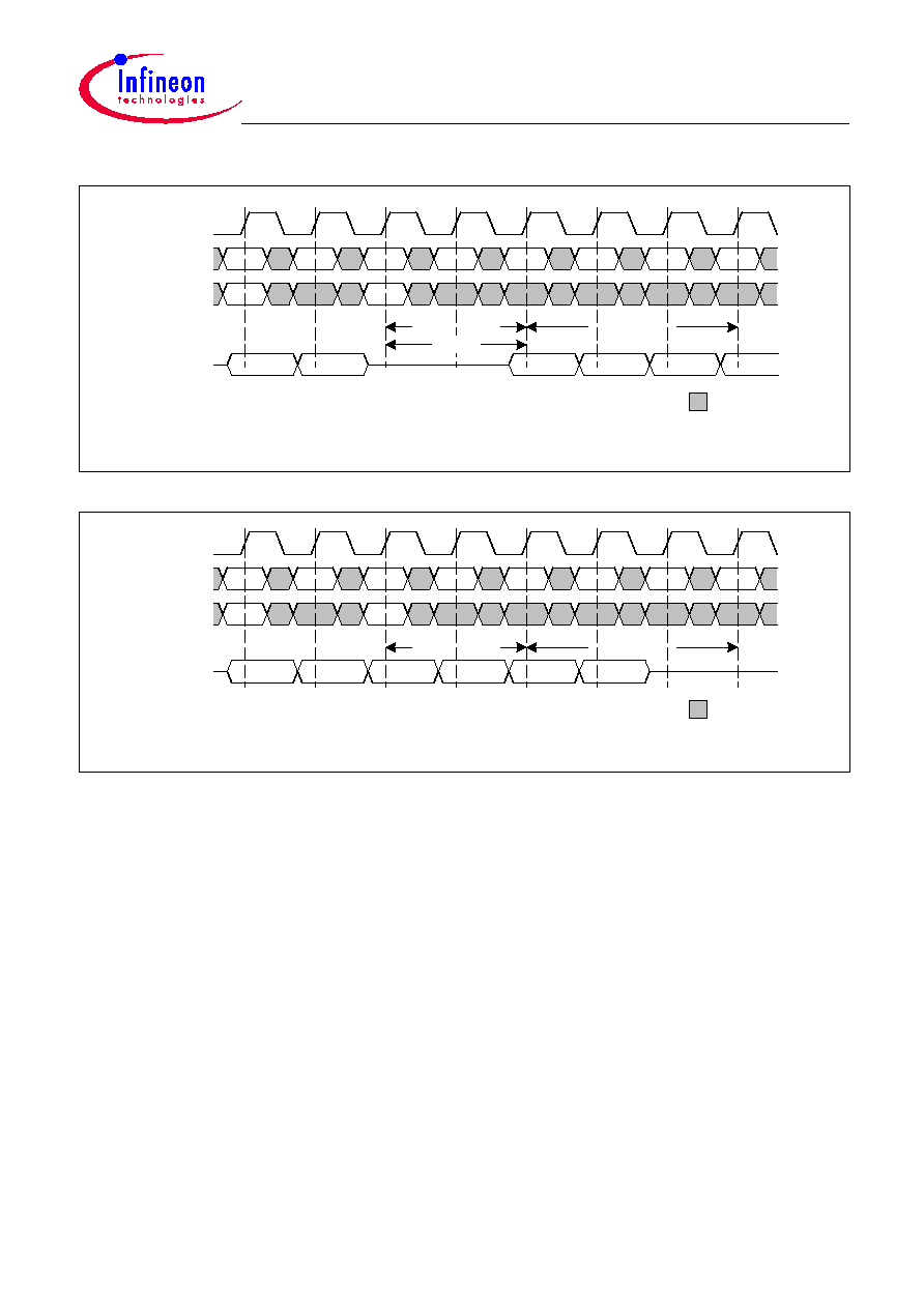
Figure 26
WRITE Burst (CAS Latency = 3)
Data for any WRITE burst may be concatenated with or truncated with a subsequent WRITE command. In either
case, a continuous flow of input data can be maintained. A WRITE command can be issued on any positive edge
of clock following the previous WRITE command. The first data element from the new burst is applied after either
the last element of a completed burst (
Figure 27
) or the last desired data element of a longer burst which is being
truncated (
Figure 28
). The new WRITE command should be issued x cycles after the first WRITE command,
where x equals the number of desired data elements.
Figure 27
Consecutive WRITE Bursts
HY[B/E]18L256160B[C/F]L-7.5
256-Mbit Mobile-RAM
Functional Description
Data Sheet
30
Rev. 1.72, 2005-07
01302004-CZ2R-J9SE
Figure 28
Random WRITE Bursts
Non-consecutive WRITE bursts are shown in
Figure 29
.
Figure 29
Non-Consecutive WRITE Bursts
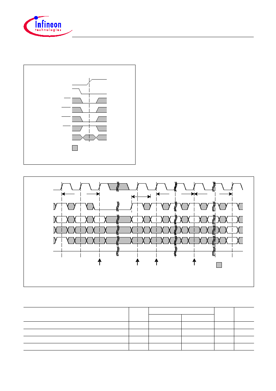
2.4.6.1
WRITE Burst Termination
Data from any WRITE burst may be truncated using the BURST TERMINATE command (see
Page 33
), provided
that Auto Precharge was not activated. The input data provided coincident with the BURST TERMINATE
command will be ignored. This is shown in
Figure 30
. The BURST TERMINATE command may be used to
terminate a full-page WRITE which does not self-terminate.
Data Sheet
31
Rev. 1.72, 2005-07
01302004-CZ2R-J9SE
HY[B/E]18L256160B[C/F]L-7.5
256-Mbit Mobile-RAM
Functional Description
Figure 30
Terminating a WRITE Burst
2.4.6.2
Clock Suspend Mode for WRITE Cycles
Clock suspend mode allows to extend any WRITE burst in progress by a variable number of clock cycles. As long
as CKE is registered LOW, the following internal clock pulse(s) will be ignored and no data will be captured, as
shown in
Figure 31
.
Figure 31
Clock Suspend Mode for WRITE Bursts
HY[B/E]18L256160B[C/F]L-7.5
256-Mbit Mobile-RAM
Functional Description
Data Sheet
32
Rev. 1.72, 2005-07
01302004-CZ2R-J9SE
2.4.6.3
WRITE - DQM Operation
DQM may be used to mask write data: when asserted HIGH, input data will be masked and no write will be
performed. The generic timing parameters as listed in
Table 11
also apply to this DQM operation. The write burst
in progress is not affected and will continue as programmed.
Figure 32
WRITE Burst - DQM Operation
2.4.6.4
WRITE to READ
A WRITE burst may be followed by, or truncated with a READ command. The READ command can be performed
to the same or a different (active) bank. With the registration of the READ command, data inputs will be ignored
and no WRITE will be performed, as shown in
Figure 33
.
Figure 33
WRITE to READ Timing
Data Sheet
33
Rev. 1.72, 2005-07
01302004-CZ2R-J9SE
HY[B/E]18L256160B[C/F]L-7.5
256-Mbit Mobile-RAM
Functional Description
2.4.6.5
WRITE to PRECHARGE
A WRITE burst may be followed by, or truncated with a PRECHARGE command to the same bank, provided that
Auto Precharge was not activated. This is shown in
Figure 34
.
The PRECHARGE command should be issued
t
WR
after the clock edge at which the last desired data element of
the WRITE burst was registered. Additionally, when truncating a WRITE burst, DQM must be pulled to mask input
data presented during
t
WR
prior to the PRECHARGE command. Following the PRE-CHARGE command, a
subsequent ACTIVE command to the same bank cannot be issued until
t
RP
is met.
In the case of a WRITE being executed to completion, a PRECHARGE command issued at the optimum time (as
described above) provides the same operation that would result from the same WRITE burst with Auto Precharge
enabled. The disadvantage of the PRECHARGE command is that it requires that the command and address
busses be available at the appropriate time to issue the command. The advantage of the PRECHARGE command
is that it can be used to truncate bursts.
Figure 34
WRITE to PRECHARGE Timing
2.4.7
BURST TERMINATE
Figure 35
BURST TERMINATE Command
The BURST TERMINATE command is used to truncate
READ or WRITE bursts (with Auto Precharge
disabled). The most recently registered READ or
WRITE command prior to the BURST TERMINATE
command will be truncated, as shown in
Figure 18
and
Figure 30
, respectively.
The BURST TERMINATE command is not allowed for
truncation of READ or WRITE bursts with Auto
Precharge enabled.
HY[B/E]18L256160B[C/F]L-7.5
256-Mbit Mobile-RAM
Functional Description
Data Sheet
34
Rev. 1.72, 2005-07
01302004-CZ2R-J9SE
2.4.8
PRECHARGE
Figure 36
PRECHARGE Command
The PRECHARGE command is used to deactivate
(close) the open row in a particular bank or the open
row in all banks. The bank(s) will be available for a
subsequent row access a specified time (
t
RP
) after the
PRECHARGE command is issued. Input A10
determines whether one or all banks are to be
precharged, and in the case where only one bank is to
be precharged, inputs BA0, BA1 select the bank.
Otherwise BA0, BA1 are treated as "Don't Care".
Once a bank has been precharged, it is in the idle state
and must be activated prior to any READ or WRITE
commands being issued to that bank. A PRECHARGE
command will be treated as a NOP if there is no open
row in that bank, or if the previously open row is already
in the process of precharging.
2.4.8.1
AUTO PRECHARGE
Auto Precharge is a feature which performs the same individual-bank precharge functions described above, but
without requiring an explicit command. This is accomplished by using A10 to enable Auto Precharge in conjunction
with a specific READ or WRITE command. A precharge of the bank/row that is addressed with the READ or
WRITE command is automatically performed upon completion of the READ or WRITE burst. Auto Precharge is
non persistent in that it is either enabled or disabled for each individual READ or WRITE command. Auto
Precharge ensures that the precharge is initiated at the earliest valid stage within a burst. The user must not issue
another command to the same bank until the precharge (
t
RP
) is completed. This is determined as if an explicit
PRECHARGE command was issued at the earliest possible time, as described for each burst type.
Table 12
Timing Parameters for PRECHARGE
Parameter
Symbol
- 7.5
Units
Notes
min.
max.
ACTIVE to PRECHARGE command period
t
RAS
45
100k
ns
1)
1) These parameters account for the number of clock cycles and depend on the operating frequency as follows:
no. of clock cycles = specified delay / clock period; round up to next integer.
WRITE recovery time
t
WR
14
≠
ns
1)
PRECHARGE command period
t
RP
19
≠
ns
1)
Data Sheet
35
Rev. 1.72, 2005-07
01302004-CZ2R-J9SE
HY[B/E]18L256160B[C/F]L-7.5
256-Mbit Mobile-RAM
Functional Description
2.4.8.2
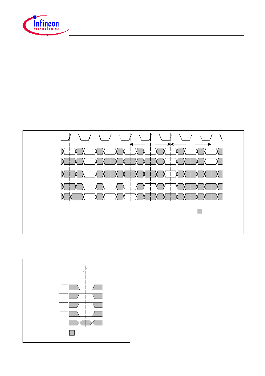
CONCURRENT AUTO PRECHARGE
A READ or WRITE burst with Auto Precharge enabled can be interrupted by a subsequent READ or WRITE
command issued to a different bank.
Figure 37
shows a READ with Auto Precharge to bank n, interrupted by a READ (with or without Auto Precharge)
to bank m. The READ to bank m will interrupt the READ to bank n, CAS latency later. The precharge to bank n
will begin when the READ to bank m is registered.
Figure 38
shows a READ with Auto Precharge to bank n, interrupted by a WRITE (with or without Auto Precharge)
to bank m. The precharge to bank n will begin when the WRITE to bank m is registered. DQM should be pulled
HIGH two clock cycles prior to the WRITE to prevent bus contention.
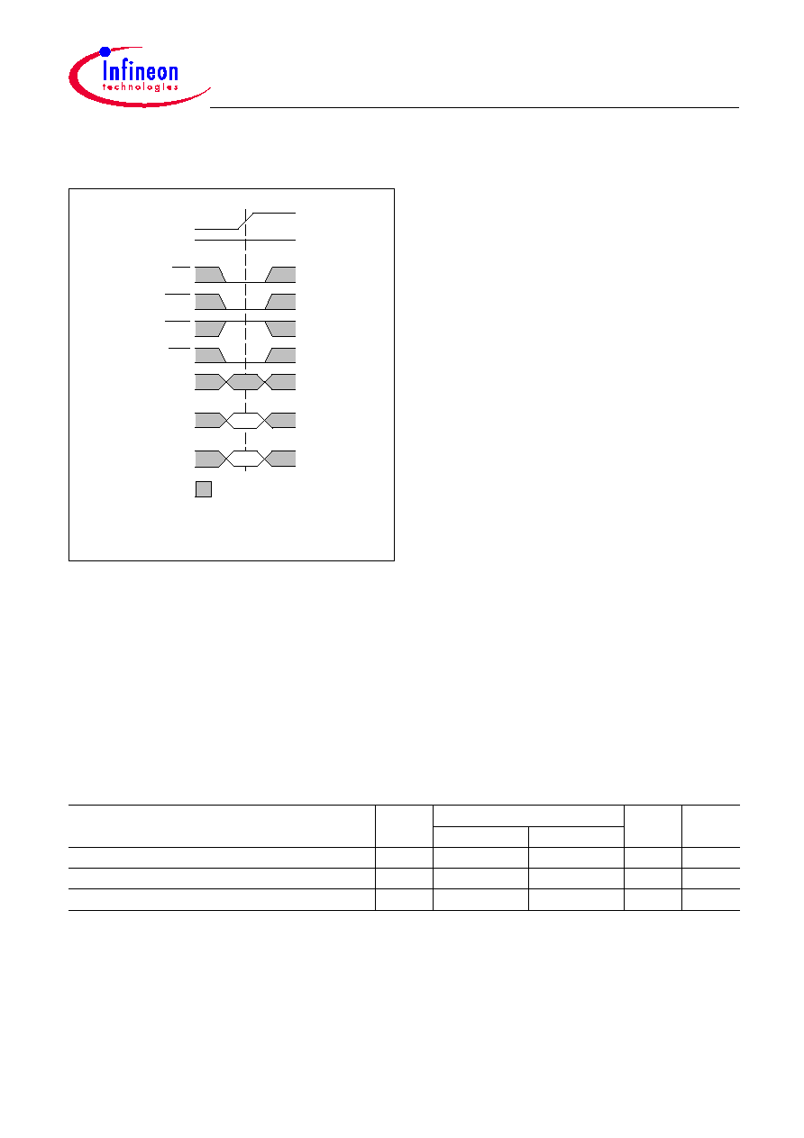
Figure 39
shows a WRITE with Auto Precharge to bank n, interrupted by a READ (with or without Auto Precharge)
to bank m. The precharge to bank n will begin
t
WR
after the new command to bank m is registered. The last valid
data-in to bank n is one clock cycle prior to the READ to bank m.
Figure 40
shows a WRITE with Auto Precharge to bank n, interrupted by a WRITE (with or without Auto
Precharge) to bank m. The precharge to bank n will begin
t
WR
after the WRITE to bank m is registered. The last
valid data-in to bank n is one clock cycle prior to the WRITE to bank m.
Figure 37
READ with Auto Precharge Interrupted by READ
Figure 38
READ with Auto Precharge Interrupted by WRITE
HY[B/E]18L256160B[C/F]L-7.5
256-Mbit Mobile-RAM
Functional Description
Data Sheet
36
Rev. 1.72, 2005-07
01302004-CZ2R-J9SE
Figure 39
WRITE with Auto Precharge Interrupted by READ
Figure 40
WRITE with Auto Precharge Interrupted by WRITE
Data Sheet
37
Rev. 1.72, 2005-07
01302004-CZ2R-J9SE
HY[B/E]18L256160B[C/F]L-7.5
256-Mbit Mobile-RAM
Functional Description
2.4.9
AUTO REFRESH and SELF REFRESH
The Mobile-RAM requires a refresh of all rows in a rolling interval. Each refresh is generated in one of two ways:
by an explicit AUTO REFRESH command, or by an internally timed event in SELF REFRESH mode.
2.4.9.1
AUTO REFRESH
Figure 41
AUTO REFRESH Command
Auto Refresh is used during normal operation of the
Mobile-RAM. The command is non persistent, so it
must be issued each time a refresh is required. A
minimum row cycle time (
t
RC
) is required between two
AUTO REFRESH commands. The same rule applies to
any access command after the auto refresh operation.
All banks must be precharged prior to the AUTO
REFRESH command.
The refresh addressing is generated by the internal
refresh controller. This makes the address bits "Don't
Care" during an AUTO REFRESH command. The
Mobile-RAM requires AUTO REFRESH cycles at an
average periodic interval of 7.8
µ
s (max.). Partial array
mode has no influence on auto refresh mode.
Figure 42
Auto Refresh
HY[B/E]18L256160B[C/F]L-7.5
256-Mbit Mobile-RAM
Functional Description
Data Sheet
38
Rev. 1.72, 2005-07
01302004-CZ2R-J9SE
2.4.9.2
SELF REFRESH
Figure 43
SELF REFRESH Entry Command
The SELF REFRESH command can be used to retain
data in the Mobile-RAM, even if the rest of the system
is powered down. When in the self refresh mode, the
Mobile-RAM retains data without external clocking. The
SELF REFRESH command is initiated like an AUTO
REFRESH command except CKE is LOW. Input
signals except CKE are "Don't Care" during SELF
REFRESH.
The procedure for exiting SELF REFRESH requires a
stable clock prior to CKE returning HIGH. Once CKE is
HIGH, NOP commands must be issued for
t
RC
because
time is required for a completion of any internal refresh
in progress.
If during normal operation burst auto refresh or user
controlled refresh is used, add 8192 auto refresh cycles
just before self refresh entry and just after self refresh
exit.
Figure 44
Self Refresh Entry and Exit
Table 13
Timing Parameters for AUTO REFRESH and SELF REFRESH
Parameter
Symbol
- 7.5
Units
Notes
min.
max.
ACTIVE to ACTIVE command period
t
RC
67
≠
ns
1)
1) These parameters account for the number of clock cycles and depend on the operating frequency as follows:
no. of clock cycles = specified delay / clock period; round up to next integer.
PRECHARGE command period
t
RP
19
≠
ns
1)
Refresh period (8192 rows)
t
REF
≠
64
ms
1)
Self refresh exit time
t
SREX
1
≠
t
CK
1)
Data Sheet
39
Rev. 1.72, 2005-07
01302004-CZ2R-J9SE
HY[B/E]18L256160B[C/F]L-7.5
256-Mbit Mobile-RAM
Functional Description
2.4.10
POWER DOWN
Figure 45
Power Down Entry Command
Power-down is entered when CKE is registered LOW
(no accesses can be in progress). If power-down
occurs when all banks are idle, this mode is referred to
as precharge power-down; if power-down occurs when
there is a row active in any bank, this mode is referred
to as active power-down. Entering power-down
deactivates the input and output buffers, excluding CLK
and CKE. CKE LOW must be maintained during power-
down.
Power-down duration is limited by the refresh
requirements of the device (
t
REF
).
The power-down state is synchronously exited when
CKE is registered HIGH (along with a NOP or
DESELECT command). One clock delay is required for
power down entry and exit.
Figure 46
Power Down Entry and Exit
2.4.10.1 DEEP POWER DOWN
The deep power down mode is an unique function on Low Power SDRAM devices with extremely low current
consumption. Deep power down mode is entered using the BURST TERMINATE command (cf.
Figure 35
) except
that CKE is LOW. All internal voltage generators inside the device are stopped and all memory data is lost in this
mode. To enter the deep power down mode all banks must be precharged.
The deep power down mode is asynchronously exited by asserting CKE HIGH. After the exit, the same command
sequence as for power-up initialization, including the 200µs initial pause, has to be applied before any other
command may be issued (cf.
Figure 3
and
Figure 4
).
HY[B/E]18L256160B[C/F]L-7.5
256-Mbit Mobile-RAM
Functional Description
Data Sheet
40
Rev. 1.72, 2005-07
01302004-CZ2R-J9SE
2.5
Function Truth Tables
Table 14
Current State Bank n - Command to Bank n
Current State
CS RAS CAS WE Command / Action
Notes
Any
H
X
X
X
DESELECT (NOP / continue previous operation)
1)2)3)4)5)6)
1) This table applies when CKEn-1 was HIGH and CKEn is HIGH and after
t
RC
has been met (if the previous state was self
refresh).
2) This table is bank-specific, except where noted, i.e., the current state is for a specific bank and the commands shown are
those allowed to be issued to that bank when in that state. Exceptions are covered in the notes below.
3) Current state definitions:
Idle:
The bank has been precharged, and
t
RP
has been met.
Row Active:
A row in the bank has been activated, and
t
RCD
has been met. No data bursts/accesses and no register
accesses are in progress.
Read:
A READ burst has been initiated, with Auto Precharge disabled, and has not yet terminated or been
terminated.
Write:
A WRITE burst has been initiated, with Auto Precharge disabled, and has not yet terminated or been
terminated.
4) The following states must not be interrupted by a command issued to the same bank. DESELECT or NOP commands, or
allowable commands to the other bank should be issued on any clock edge occurring during these states. Allowable
commands to the other bank are determined by its current state and according to
Table 15
.
Precharging:
Starts with registration of a PRECHARGE command and ends when
t
RP
is met. Once
t
RP
is met, the bank
is in the "idle" state.
Row Activating: Starts with registration of an ACTIVE command and ends when
t
RCD
is met. Once
t
RCD
is met, the bank
is in the "row active" state.
Read with AP
Enabled:
Starts with registration of a READ command with Auto Precharge enabled and ends when
t
RP
has been
met. Once
t
RP
is met, the bank is in the idle state.
Write with AP
Enabled:
Starts with registration of a WRITE command with Auto Precharge enabled and ends when
t
RP
has been
met. Once
t
RP
is met, the bank is in the idle state.
L
H
H
H
NO OPERATION (NOP / continue previous operation)
1) to 6)
Idle
L
L
H
H
ACTIVE (select and activate row)
1) to 6)
L
L
L
H
AUTO REFRESH
1) to 7)
L
L
L
L
MODE REGISTER SET
1) to 7)
L
L
H
L
PRECHARGE
1) to 6), 8)
Row Active
L
H
L
H
READ (select column and start READ burst)
1) to 6), 9)
L
H
L
L
WRITE (select column and start WRITE burst)
1) to 6), 9)
L
L
H
L
PRECHARGE (deactivate row in bank or banks)
1) to 6), 10)
Read
(Auto-
Precharge
Disabled)
L
H
L
H
READ (select column and start new READ burst)
1) to 6), 9)
L
H
L
L
WRITE (select column and start new WRITE burst)
1) to 6), 9)
L
L
H
L
PRECHARGE (truncate READ burst, start precharge)
1) to 6), 10)
L
H
H
L
BURST TERMINATE
1) to 6), 11)
Write
(Auto-
Precharge
Disabled)
L
H
L
H
READ (select column and start READ burst)
1) to 6), 9)
L
H
L
L
WRITE (select column and start WRITE burst)
1) to 6), 9)
L
L
H
L
PRECHARGE (truncate WRITE burst, start precharge)
1) to 6), 10)
L
H
H
L
BURST TERMINATE
1) to 6), 11)

Data Sheet
41
Rev. 1.72, 2005-07
01302004-CZ2R-J9SE
HY[B/E]18L256160B[C/F]L-7.5
256-Mbit Mobile-RAM
Functional Description
5) The following states must not be interrupted by any executable command; DESELECT or NOP commands must be applied
on each positive clock edge during these states.
Refreshing:
Starts with registration of an AUTO REFRESH command and ends when
t
RC
is met. Once
t
RC
is met, the
SDRAM is in the "all banks idle" state.
Accessing Mode
Register:
Starts with registration of a MODE REGISTER SET command and ends when
t
MRD
has been met. Once
t
MRD
is met, the SDRAM is in the "all banks idle" state.
Precharging All: Starts with registration of a PRECHARGE ALL command and ends when
t
RP
is met. Once
t
RP
is met, all
banks are in the idle state.
6) All states and sequences not shown are illegal or reserved.
7) Not bank-specific; requires that all banks are idle and no bursts are in progress.
8) Same as NOP command in that state.
9) READs or WRITEs listed in the Command/Action column include READs or WRITEs with Auto Precharge enabled and
READs or WRITEs with Auto Precharge disabled.
10) May or may not be bank-specific; if multiple banks are to be precharged, each must be in a valid state for precharging.
11) Not bank-specific; BURST TERMINATE affects the most recent READ or WRITE burst, regardless of bank.
Table 15
Current State Bank n - Command to Bank m (different bank)
Current State
CS RAS CAS WE Command / Action
Notes
Any
H
X
X
X
DESELECT (NOP / continue previous operation)
1)2)3)4)5)6)
1) This table applies when CKEn-1 was HIGH and CKEn is HIGH and after
t
RC
has been met (if the previous state was Self
Refresh).
2) This table describes alternate bank operation, except where noted, i.e., the current state is for bank n and the commands
shown are those allowed to be issued to bank m (assuming that bank m is in such a state that the given command is
allowable). Exceptions are covered in the notes below.
L
H
H
H
NO OPERATION (NOP / continue previous operation)
1) to 6)
Idle
X
X
X
X
Any command otherwise allowed to bank n
1) to 6)
Row Activating,
Active, or
Precharging
L
L
H
H
ACTIVE (select and activate row)
1) to 6)
L
H
L
H
READ (select column and start READ burst)
1) to 7)
L
H
L
L
WRITE (select column and start WRITE burst)
1) to 7)
L
L
H
L
PRECHARGE (deactivate row in bank or banks)
1) to 6)
Read (Auto-
Precharge
Disabled)
L
L
H
H
ACTIVE (select and activate row)
1) to 6)
L
H
L
H
READ (select column and start READ burst)
1) to 7)
L
H
L
L
WRITE (select column and start WRITE burst)
1) to 8)
L
L
H
L
PRECHARGE (deactivate row in bank or banks)
1) to 6)
Write (Auto-
Precharge
Disabled)
L
L
H
H
ACTIVE (select and activate row)
1) to 6)
L
H
L
H
READ (select column and start READ burst)
1) to 7)
L
H
L
L
WRITE (select column and start WRITE burst)
1) to 7)
L
L
H
L
PRECHARGE (deactivate row in bank or banks)
1) to 6)
Read
(with Auto-
Precharge)
L
L
H
H
ACTIVE (select and activate row)
1) to 6)
L
H
L
H
READ (select column and start READ burst)
1) to 7), 9)
L
H
L
L
WRITE (select column and start WRITE burst)
1) to 9)
L
L
H
L
PRECHARGE (deactivate row in bank or banks)
1) to 6)
Write
(with Auto-
Precharge)
L
L
H
H
ACTIVE (select and activate row)
1) to 6)
L
H
L
H
READ (select column and start READ burst)
1) to 7), 9)
L
H
L
L
WRITE (select column and start WRITE burst)
1) to 7), 9)
L
L
H
L
PRECHARGE (deactivate row in bank or banks)
1) to 6)

HY[B/E]18L256160B[C/F]L-7.5
256-Mbit Mobile-RAM
Functional Description
Data Sheet
42
Rev. 1.72, 2005-07
01302004-CZ2R-J9SE
3) Current state definitions:
Idle:
The bank has been precharged, and
t
RP
has been met.
Row Active:
A row in the bank has been activated, and
t
RCD
has been met. No data bursts/accesses and no register
accesses are in progress.
Read:
A READ burst has been initiated, with Auto Precharge disabled, and has not yet terminated or been
terminated.
Write:
A WRITE burst has been initiated, with Auto Precharge disabled, and has not yet terminated or been
terminated.
Read with AP
Enabled:
Starts with registration of a READ command with Auto Precharge enabled and ends when
t
RP
has been
met. Once
t
RP
is met, the bank is in the idle state.
Write with AP
Enabled:
Starts with registration of a WRITE command with Auto Precharge enabled and ends when
t
RP
has been
met. Once
t
RP
is met, the bank is in the idle state.
4) AUTO REFRESH, SELF REFRESH and MODE REGISTER SET commands may only be issued when all banks are idle.
5) A BURST TERMINATE command cannot be issued to another bank; it applies to the bank represented by the current state
only.
6) All states and sequences not shown are illegal or reserved.
7) READs or WRITEs listed in the Command/Action column include READs or WRITEs with Auto Precharge enabled and
READs or WRITEs with Auto Precharge disabled.
8) Requires appropriate DQM masking.
9) Concurrent Auto Precharge: bank n will start precharging when its burst has been interrupted by a READ or WRITE
command to bank m.
Table 16
Truth Table - CKE
CKEn-1
CKEn
Current State
Command
Action
Notes
L
L
Power Down
X
Maintain Power Down
1)2)3)4)
1) CKEn is the logic state of CKE at clock edge n; CKEn-1 was the state of CKE at the previous clock edge.
2) Current state is the state immediately prior to clock edge n.
3) COMMAND n is the command registered at clock edge n; ACTION n is a result of COMMAND n.
4) All states and sequences not shown are illegal or reserved.
Self Refresh
X
Maintain Self Refresh
1) to 4)
Clock Suspend
X
Maintain Clock Suspend
1) to 4)
Deep Power Down
X
Maintain Deep Power
Down
1) to 4)
L
H
Power Down
DESELECT or NOP
Exit Power Down
1) to 4)
Self Refresh
DESELECT or NOP
Exit Self Refresh
1) to 5)
5) DESELECT or NOP commands should be issued on any clock edges occurring during
t
RC
period.
Clock Suspend
X
Exit Clock Suspend
1) to 4)
Deep Power Down
X
Exit Deep Power Down
1) to 4), 6)
6) Exit from DEEP POWER DOWN requires the same command sequence as for power-up initialization.
H
L
All Banks Idle
DESELECT or NOP
Enter Precharge Power
Down
1) to 4)
Bank(s) Active
DESELECT or NOP
Enter Active Power Down
1) to 4)
All Banks Idle
AUTO REFRESH
Enter Self Refresh
1) to 4)
Read / Write burst
(valid)
Enter Clock Suspend
1) to 4)
H
H
see
Table 14
and
Table 15
1) to 4)
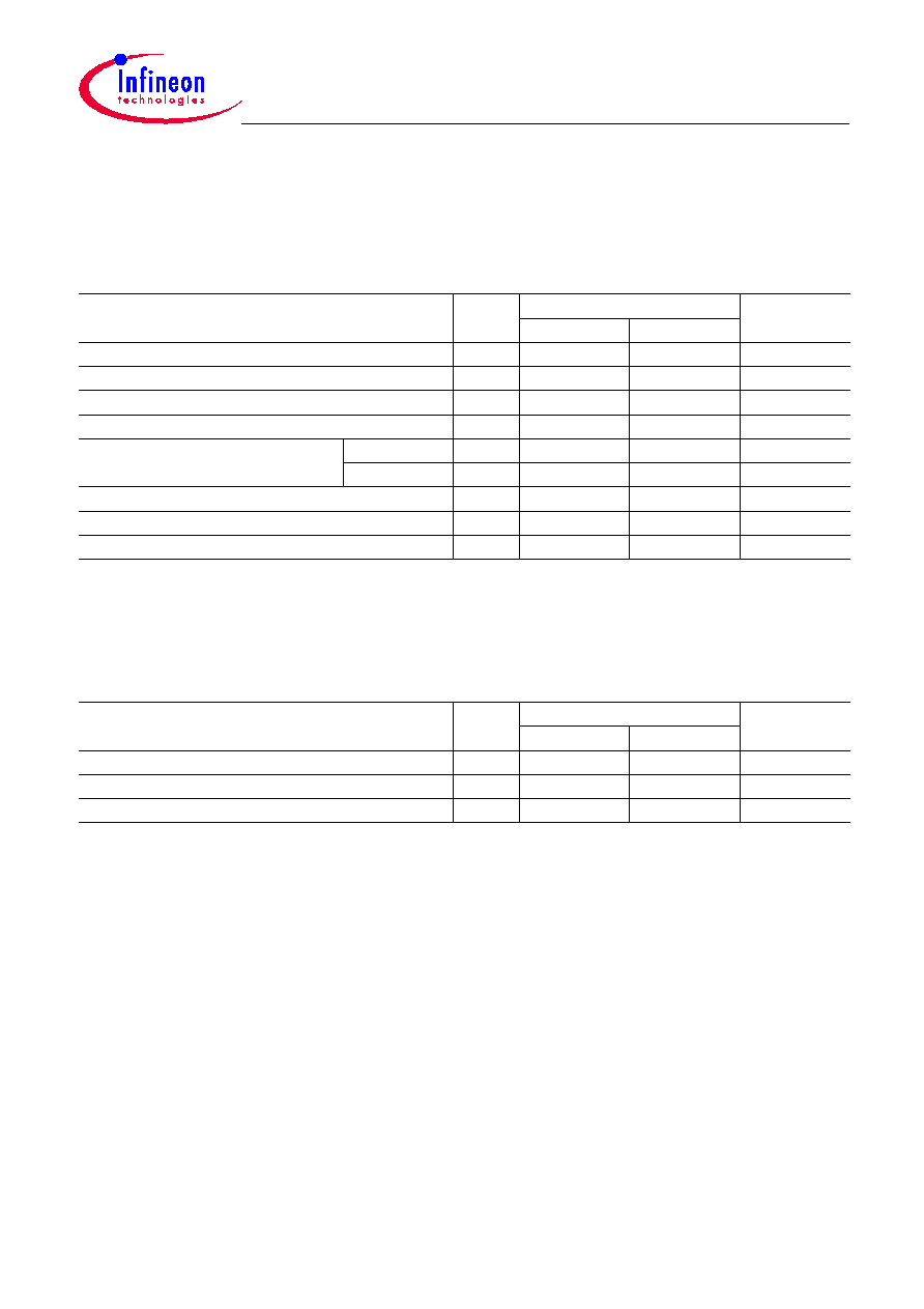
Data Sheet
43
Rev. 1.72, 2005-07
01302004-CZ2R-J9SE
HY[B/E]18L256160B[C/F]L-7.5
256-Mbit Mobile-RAM
Electrical Characteristics
3
Electrical Characteristics
3.1
Operating Conditions
Attention: Stresses above those listed here may cause permanent damage to the device. Exposure to
absolute maximum rating conditions for extended periods may affect device reliability.
Maximum ratings are absolute ratings; exceeding only one of these values may cause
irreversible damage to the integrated circuit.
Table 17
Absolute Maximum Ratings
Parameter
Symbol
Values
Unit
min.
max.
Power Supply Voltage
V
DD
-0.3
2.7
V
Power Supply Voltage for Output Buffer
V
DDQ
-0.3
2.7
V
Input Voltage
V
IN
-0.3
V
DDQ
+ 0.3
V
Output Voltage
V
OUT
-0.3
V
DDQ
+ 0.3
V
Operation Case Temperature
Commercial
T
C
0
+70
∞
C
Extended
T
C
-25
+85
∞
C
Storage Temperature
T
STG
-55
+150
∞
C
Power Dissipation
P
D
≠
0.7
W
Short Circuit Output Current
I
OUT
≠
50
mA
Table 18
Pin Capacitances
1)2)
1) These values are not subject to production test but verified by device characterization.
2) Input capacitance is measured according to JEP147 with VDD, VDDQ applied and all other pins (except the pin under test)
floating. DQ's should be in high impedance state. This may be achieved by pulling CKE to low level.
Parameter
Symbol
Values
Unit
min.
max.
Input capacitance: CLK
C
I1
1.5
3.0
pF
Input capacitance: all other input pins
C
I2
1.5
3.0
pF
Input/Output capacitance: DQ
C
IO
3.0
5.0
pF
HY[B/E]18L256160B[C/F]L-7.5
256-Mbit Mobile-RAM
Electrical Characteristics
Data Sheet
44
Rev. 1.72, 2005-07
01302004-CZ2R-J9SE
Table 19
Electrical Characteristics
1)
1) 0
∞
C
T
C
70
∞
C (comm.); -25
∞
C
T
C
85
∞
C (ext.); all voltages referenced to
V
SS
.
V
SS
and
V
SSQ
must be at same potential.
Parameter
Symbol
Values
Unit
Notes
min.
max.
Power Supply Voltage
V
DD
1.65
1.95
V
≠
Power Supply Voltage for DQ Output Buffer
V
DDQ
1.65
1.95
V
≠
Input high voltage
V
IH
0.8
◊
V
DDQ
V
DDQ
+ 0.3
V
2)
2)
V
IH
may overshoot to
V
DD
+ 0.8 V for pulse width < 4 ns;
V
IL
may undershoot to -0.8 V for pulse width < 4 ns.
Pulse width measured at 50% with amplitude measured between peak voltage and DC reference level.
Input low voltage
V
IL
-0.3
0.3
V
2)
Output high voltage (
I
OH
= -0.1 mA)
V
OH
V
DDQ
- 0.2
≠
V
≠
Output low voltage (
I
OL
= 0.1 mA)
V
OL
≠
0.2
V
≠
Input leakage current
I
IL
-1.0
1.0
µ
A
≠
Output leakage current
I
OL
-1.5
1.5
µ
A
≠
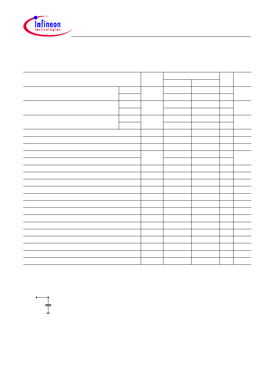
Data Sheet
45
Rev. 1.72, 2005-07
01302004-CZ2R-J9SE
HY[B/E]18L256160B[C/F]L-7.5
256-Mbit Mobile-RAM
Electrical Characteristics
3.2
AC Characteristics
Table 20
AC Characteristics
1)2)3)4)
1) 0
∞
C
T
C
70
∞
C (comm.); -25
∞
C
T
C
85
∞
C (ext.);
V
DD
=
V
DDQ
= 1.65V to 1.95V;
2) All parameters assumes proper device initialization.
3) AC timing tests measured at 0.9 V.
4) The transition time
t
T
is measured between
V
IH
and
V
IL
; all AC characteristics assume
t
T
= 1 ns.
Parameter
Symbol
- 7.5
Unit Notes
min.
max.
Clock cycle time
CL = 3
t
CK
7.5
--
ns
--
CL = 2
9.5
--
ns
Clock frequency
CL = 3
f
CK
--
133
MHz
--
CL = 2
--
105
MHz
Access time from CLK
CL = 3
t
AC
--
5.4
ns
5)6)
5) Specified
t
AC
and
t
OH
parameters are measured with a 30 pF capacitive load only as shown below:
6) If
t
T
(CLK) > 1 ns, a value of (
t
T
/2 - 0.5) ns has to be added to this parameter.
CL = 2
--
6.0
ns
Clock high-level width
t
CH
2.5
--
ns
--
Clock low-level width
t
CL
2.5
--
ns
--
Address, data and command input setup time
t
IS
1.5
--
ns
7)
7) If
t
T
> 1 ns, a value of [0.5 x (
t
T
- 1)] ns has to be added to this parameter.
Address and command input hold time
t
IH
0.5
--
ns
7)
Data (DQ) input hold time
0.8
--
MODE REGISTER SET command period
t
MRD
2
--
t
CK
--
DQ low-impedance time from CLK
t
LZ
1.0
≠
ns
--
DQ high-impedance time from CLK
t
HZ
3.0
7.0
ns
--
Data out hold time
t
OH
2.5
--
ns
5)6)
DQM to DQ High-Z delay (READ Commands)
t
DQZ
--
2
t
CK
--
DQM write mask latency
t
DQW
0
--
t
CK
--
ACTIVE to ACTIVE command period
t
RC
67
--
ns
8)
8) These parameter account for the number of clock cycles and depend on the operating frequency, as follows:
no. of clock cycles = specified delay / clock period; round up to next integer.
ACTIVE to READ or WRITE delay
t
RCD
19
--
ns
8)
ACTIVE bank A to ACTIVE bank B delay
t
RRD
15
--
ns
8)
ACTIVE to PRECHARGE command period
t
RAS
45
100k
ns
8)
WRITE recovery time
t
WR
14
--
ns
9)
9) The write recovery time of
t
WR
= 14 ns allows the use of one clock cycle for the write recovery time when
f
CK
72 MHz.
With
f
CK
> 72 MHz two clock cycles for
t
WR
are mandatory. Infineon Technologies recommends to use two clock cycles for
the write recovery time in all applications.
PRECHARGE command period
t
RP
19
--
ns
8)
Refresh period (8192 rows)
t
REF
--
64
ms
--
Self refresh exit time
t
SREX
1
--
t
CK
--
30 pF
I/O
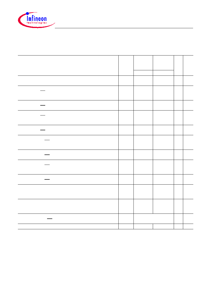
HY[B/E]18L256160B[C/F]L-7.5
256-Mbit Mobile-RAM
Electrical Characteristics
Data Sheet
46
Rev. 1.72, 2005-07
01302004-CZ2R-J9SE
3.3
Operating Currents
Table 21
Maximum Operating Currents
1)
1) 0
∞
C
T
C
70
∞
C (comm.); -25
∞
C
T
C
85
∞
C (ext.);
V
DD
=
V
DDQ
= 1.65V to 1.95V;
Recommended Operating Conditions unless otherwise noted
Parameter & Test Conditions
Symbol Values for
HY[B/E]...
160B[C/F]
Values for
HYE...
160B[C/F]L
Unit Note
- 7.5
- 7.5
Operating current:
one bank:
active / read / precharge, BL = 1,
t
RC
=
t
RCmin
I
DD1
60
60
mA
2)3)
2) These values are measured with
t
CK
= 7.5 ns
3) All parameters are measured with no output loads.
Precharge power-down standby current:
all banks idle, CS
V
IHmin
, CKE
V
ILmax
,
inputs changing once every two clock cycles
I
DD2P
0.6
0.4
mA
2)
Precharge power-down standby current with clock stop:
all banks idle, CS
V
IHmin
, CKE
V
ILmax
, all inputs stable
I
DD2PS
0.5
0.35
mA
≠
Precharge non power-down standby current:
all banks idle, CS
V
IHmin
, CKE
V
IHmin
,
inputs changing once every two clock cycles
I
DD2N
13
13
mA
2)
Precharge non power-down standby current with clock stop:
all banks idle, CS
V
IHmin
, CKE
V
IHmin
, all inputs stable
I
DD2NS
1.0
1.0
mA
≠
Active power-down standby current:
one bank active, CS
V
IHmin
, CKE
V
ILmax
,
inputs changing once every two clock cycles
I
DD3P
1.0
1.0
mA
2)
Active power-down standby current with clock stop:
one bank active, CS
V
IHmin
, CKE
V
ILmax
, all inputs stable
I
DD3PS
0.75
0.5
mA
≠
Active non power-down standby current:
one bank active, CS
V
IHmin
, CKE
V
IHmin
,
inputs changing once every two clock cycles
I
DD3N
15
15
mA
2)
Active non power-down standby current with clock stop:
one bank active, CS
V
IHmin
, CKE
V
IHmin
, all inputs stable
I
DD3NS
1.5
1.5
mA
≠
Operating burst read current:
all banks active; continuous burst read,
inputs changing once every two clock cycles
I
DD4
45
45
mA
2)3)
Auto-Refresh current:
t
RC
=
t
RCmin
, "burst refresh",
inputs changing once every two clock cycles
I
DD5
90
90
mA
2)
Self Refresh current:
self refresh mode, CS
V
IHmin
, CKE
V
ILmax
, all inputs stable
I
DD6
see
Table 22
≠
Deep Power Down current
I
DD7
20
20
µ
A
≠
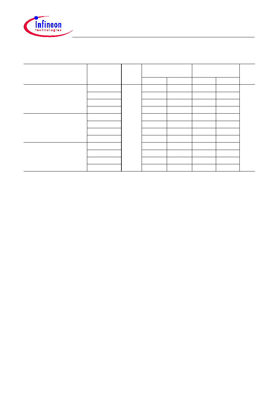
Data Sheet
47
Rev. 1.72, 2005-07
01302004-CZ2R-J9SE
HY[B/E]18L256160B[C/F]L-7.5
256-Mbit Mobile-RAM
Electrical Characteristics
Table 22
Self Refresh Currents
1)2)
1) 0
∞
C
T
C
70
∞
C (comm.); -25
∞
C
T
C
85
∞
C (ext.);
V
DD
=
V
DDQ
= 1.65V to 1.95V
2) The On-Chip Temperature Sensor (OCTS) adjusts the refresh rate in self refresh mode to the component's actual
temperature with a much finer resolution than supported by the 4 distinct temperature levels as defined by JEDEC for
TCSR. At production test the sensor is calibrated, and IDD6 max. current is measured at 85∞C. Typ. values are obtained
from device characterization.
Parameter & Test
Conditions
Max.
Temperature
Symbol
Values for
HY[B/E]256160B[C/F]
Values for
HYE256160B[C/F]L
Unit
typ.
max.
typ.
max.
Self Refresh Current:
Self refresh mode,
full array activation
(PASR = 000)
85
∞
C
I
DD6
510
600
430
450
µ
A
70
∞
C
340
≠
285
≠
45
∞
C
225
≠
190
≠
25 ∞C
205
≠
175
≠
Self Refresh Current:
Self refresh mode,
half array activation
(PASR = 001)
85
∞
C
400
470
305
320
70
∞
C
285
≠
220
≠
45 ∞C
200
≠
155
≠
25
∞
C
180
≠
140
≠
Self Refresh Current:
Self refresh mode,
quarter array activation
(PASR = 010)
85
∞
C
340
400
245
260
70
∞
C
250
≠
180
≠
45
∞
C
185
≠
135
≠
25 ∞C
170
≠
120
≠

HY[B/E]18L256160B[C/F]L-7.5
256-Mbit Mobile-RAM
Electrical Characteristics
Data Sheet
48
Rev. 1.72, 2005-07
01302004-CZ2R-J9SE
3.4
Pull-up and Pull down Characteristics
The above characteristics are specified under nominal process variation / condition
Temperature (
T
j
): Nominal = 50
∞
C,
V
DDQ
: Nominal = 1.80 V
Table 23
Half Drive Strength and Full Drive Strength
Voltage
(V)
Half Drive Strength
Full Drive Strength
Pull-Down Current (mA) Pull-Up Current (mA) Pull-Down Current (mA) Pull-Up Current (mA)
Nominal
Low
Nominal
High
Nominal
Low
Nominal
High
Nominal
Low
Nominal
High
Nominal
Low
Nominal
High
0.00
0.0
0.0
-19.7
-33.4
0.0
0.0
-39.3
-66.7
0.40
15.1
20.5
-18.8
-32.0
30.2
41.0
-37.6
-63.9
0.65
20.3
28.5
-18.2
-31.0
40.5
57.0
-36.4
-61.9
0.85
22.0
32.0
-17.6
-29.9
43.9
64.0
-35.1
-59.8
1.00
22.6
33.5
-16.7
-28.7
45.2
67.0
-33.3
-57.3
1.40
23.5
35.0
-9.4
-20.4
46.9
70.0
-18.8
-40.7
1.50
23.6
35.3
-6.6
-17.1
47.2
70.5
-13.2
-34.1
1.65
23.8
35.5
-1.8
-11.4
47.5
71.0
-3.5
-22.7
1.80
23.9
35.7
3.8
-4.8
47.7
71.4
7.5
-9.6
1.95
24.0
35.9
9.8
2.5
48.0
71.8
19.6
5.0
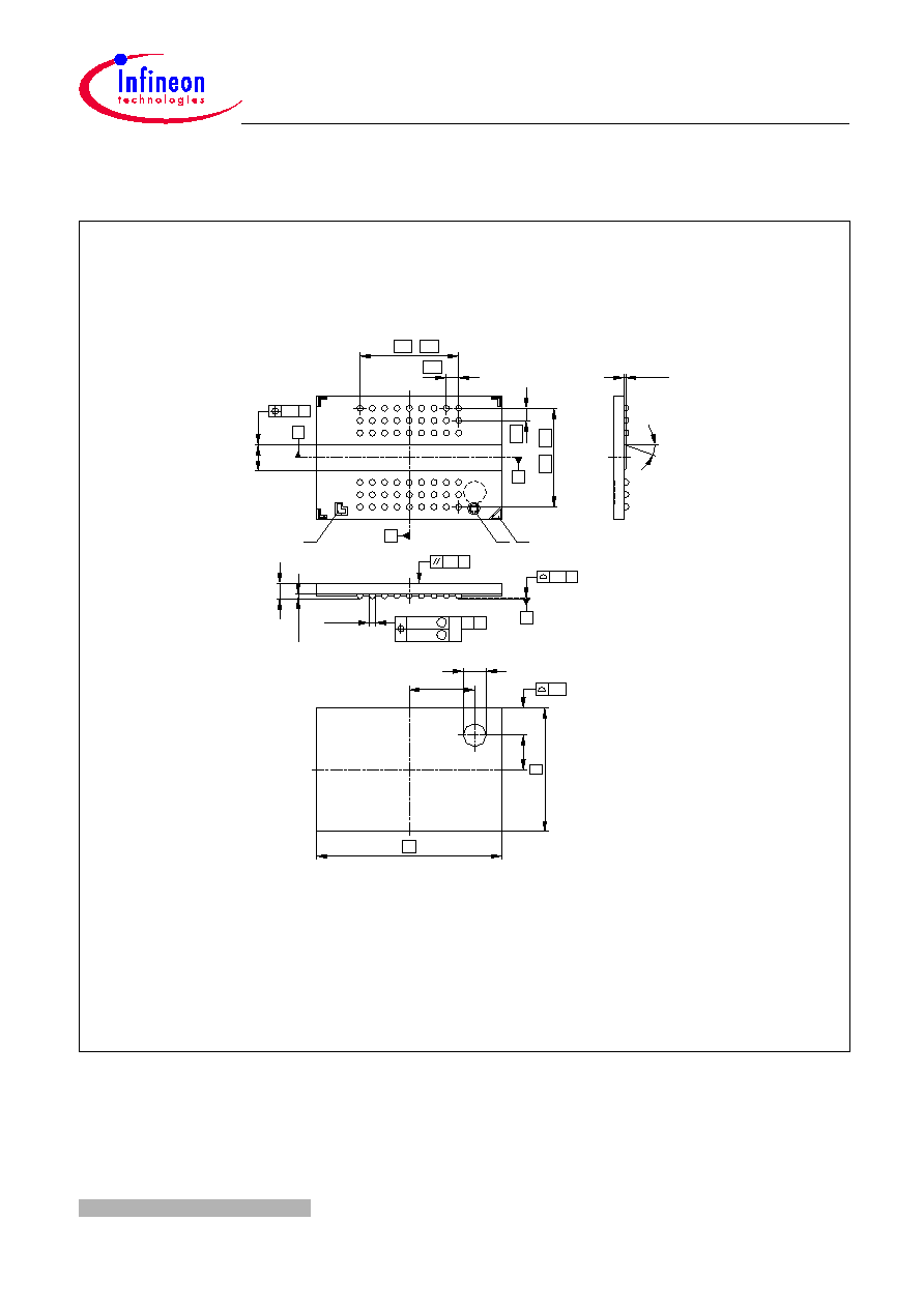
Data Sheet
49
Rev. 1.72, 2005-07
01302004-CZ2R-J9SE
HY[B/E]18L256160B[C/F]L-7.5
256-Mbit Mobile-RAM
Package Outlines
4
Package Outlines
Figure 47
P-VFBGA-54-2 (Plastic Very Thin Fine Ball Grid Array Package)
B
4)
A
4)
8 x 0.8 = 6.4
0.8
+0.01
0.12
-0.04
20∞
±5∞
2)
1)
3)
D
5)
1.7
±0.03
D
0.3
0.8
8 x 0.8 = 6.4
SEATING PLANE
C
C
0.1
C
0.1
-0.2
1.0
0.31
±0.03
A
54x
0.41
±0.03
¯0.07
¯0.12
C
M
M
B
5) Middle of Ball Matrix
4) Middle of Packages Edges
2) Die Sort Fiducial
3) Bad Unit Marking (BUM)
1) A1 Marking Ballside
1.5
12
4.25
2.24
8
2)
0.2
SMD = Surface Mounted Device
You can find all of our packages, sorts of packing and others in our
Infineon Internet Page "Products":
http://www.infineon.com/products
.
Dimensions in mm

Published by Infineon Technologies AG
w w w . i n f i n e o n . c o m