Data Book
1
9.00
HYR 16xx40G/HYR 18xx40G
Rambus RIMM Modules
Direct RDRAM RIMM Modules
(with 288 Mbit RDRAMs)
Overview
The Direct Rambus
TM
RIMM
TM
module is a general purpose high-performance memory subsystem
suitable for use in a broad range of applications including computer memory, personal computers,
workstations, and other applications where high bandwidth and low latency are required.
The Direct Rambus RIMM module consists of 288 Mbit Direct Rambus DRAM (Direct RDRAMTM)
devices. These are extremely high-speed CMOS DRAMs organized as 16M words by 18 bits. The
use of Rambus Signaling Level (RSL) technology permits 600 MHz to 800 MHz transfer rates while
using conventional system and board design technologies. Direct RDRAM devices are capable of
sustained data transfers at 1.25 ns per two bytes (10 ns per sixteen bytes).
The RDRAM architecture enables the highest sustained bandwidth for multiple, simultaneous,
randomly addressed, memory transactions. The separate control and data buses with independent
row and column control yield over 95% bus efficiency. The RDRAM's 32-bank architecture supports
up to four simultaneous transactions per device.
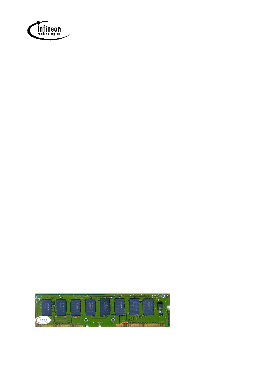
Form Factor
The Rambus RIMM modules are offered in a 184-pad 1 mm edge connector pad pitch form factor
suitable for 184 contact RIMM connectors. The RIMM module is suitable for desktop and other
system applications. The next figure shows an eight device Rambus RIMM module without heat
spreader.
Features
∑ High speed 800, 711 & 600 MHz RDRAM
storage
∑ 184 edge connector pads with 1 mm pad
spacing
∑ Maximum module PCB size:
133.5 mm
◊
31.75 mm
◊
1.37 mm
(5.25"
◊
1.25"
◊
0.05")
∑ Each RDRAM has 32 banks, for a total of
512, 256 or 128 banks on each 512/576 MB,
256/288MB or 128/144 MB module
respectively.
∑ Gold plated edge connector pad contacts
∑ Serial Presence Detect (SPD) support
∑ Operates from a 2.5 V supply (± 5%)
∑ Low power and powerdown self refresh
modes
∑ Separate Row and Column buses for higher
efficiency
Fig.1 : Rambus RIMM module
(without heat spreader)
,
HYR 16xx40G/HYR 18xx40G
Rambus RIMM Modules
Data Book
5
9.00
Module Connector Pad Description
Signal
Module Connector Pads
I/O
Type
Description
GND
A1, A3, A5, A7, A9, A11,
A13, A15, A17, A19, A21,
A23, A25, A27, A29, A31,
A33, A39, A52, A60, A62,
A64, A66, A68, A70, A72,
A74, A76, A78, A80, A82,
A84, A86, A88, A90, A92,
B1, B3, B5, B7, B9, B11,
B13, B15, B17, B19, B21,
B23, B25, B27, B29, B31,
B33, B39, B52, B60, B62,
B64, B66, B68, B70, B72,
B74, B76, B78, B80, B82,
B84, B86, B88, B90, B92
≠
≠
Ground reference for RDRAM core
and interface. 72 PCB connector
pads.
LCFM
B10
I
RSL
Clock from master. Interface clock
used for receiving RSL signals from
the Channel. Positive polarity.
LCFMN
B12
I
RSL
Clock from master. Interface clock
used for receiving RSL signals from
the Channel. Negative polarity.
LCMD
B34
I
V
CMOS
Serial Command used to read from
and write to the control registers.
Also used for power management.
LCOL4 ...
LCOL0
A20, B20, A22, B22, A24
I
RSL
Column bus. 5-bit bus containing
control and address information for
column accesses.
LCTM
A14
I
RSL
Clock to master. Interface clock
used for transmitting RSL signals to
the Channel. Positive polarity.
LCTMN
A12
I
RSL
Clock to master. Interface clock
used for transmitting RSL signals to
the Channel. Negative polarity.
LDQA8 ...
LDQA0
A2, B2, A4, B4, A6, B6,
A8, B8, A10
I/O
RSL
Data bus A. A 9-bit bus carrying a
byte of read or write data between
the Channel and the RDRAM.
LDQA8 is non-functional on
modules with x16 RDRAM devices.