 | –≠–ª–µ–∫—Ç—Ä–æ–Ω–Ω—ã–π –∫–æ–º–ø–æ–Ω–µ–Ω—Ç: IDP18E120 | –°–∫–∞—á–∞—Ç—å:  PDF PDF  ZIP ZIP |
2003-07-31
Rev.2
Page 1
IDP18E120
IDB18E120
Fast Switching EmCon Diode
Product Summary
V
RRM
1200
V
I
F
18
A
V
F
1.65
V
T
jmax
150
∞C
Feature
∑ 1200 V EmCon technology
∑ Fast recovery
∑ Soft switching
∑ Low reverse recovery charge
∑ Low forward voltage
∑ Easy paralleling
P-TO220-3.SMD
P-TO220-2-2.
Pin 1
PIN 2
PIN 3
C
A
-
NC
C
A
Marking
D18E120
D18E120
Type
Package
Ordering Code
IDP18E120
P-TO220-2-2.
Q67040-S4493
IDB18E120
P-TO220-3.SMD Q67040-S4387
Maximum Ratings, at T
j
= 25 ∞C, unless otherwise specified
Parameter
Symbol
Value
Unit
Repetitive peak reverse voltage
V
RRM
1200
V
Continous forward current
T
C
=25∞C
T
C
=90∞C
I
F
31
19.8
A
Surge non repetitive forward current
T
C
=25∞C, t
p
=10 ms, sine halfwave
I
FSM
78
Maximum repetitive forward current
T
C
=25∞C, t
p
limited by T
jmax
, D=0.5
I
FRM
47
Power dissipation
T
C
=25∞C
T
C
=90∞C
P
tot
113
54
W
Operating and storage temperature
T
j ,
T
stg
-55...+150
∞C
Soldering temperature
1.6mm(0.063 in.) from case for 10s
T
S
260
∞C
2003-07-31
Rev.2
Page 2
IDP18E120
IDB18E120
Thermal Characteristics
Parameter
Symbol
Values
Unit
min.
typ.
max.
Characteristics
Thermal resistance, junction - case
R
thJC
-
-
1.1
K/W
Thermal resistance, junction - ambient, leaded
R
thJA
-
-
62
SMD version, device on PCB:
@ min. footprint
@ 6 cm
2
cooling area
1)
R
thJA
-
-
-
35
62
-
Electrical Characteristics, at T
j
= 25 ∞C, unless otherwise specified
Parameter
Symbol
Values
Unit
min.
typ.
max.
Static Characteristics
Reverse leakage current
V
R
=1200V, T
j
=25∞C
V
R
=1200V, T
j
=150∞C
I
R
-
-
-
-
100
1400
µA
Forward voltage drop
I
F
=18A, T
j
=25∞C
I
F
=18A, T
j
=150∞C
V
F
-
-
1.65
1.7
2.15
-
V
1Device on 40mm*40mm*1.5mm epoxy PCB FR4 with 6cm≤ (one layer, 70 µm thick) copper area for drain
connection. PCB is vertical without blown air.

2003-07-31
Rev.2
Page 3
IDP18E120
IDB18E120
Electrical Characteristics, at T
j
= 25 ∞C, unless otherwise specified
Parameter
Symbol
Values
Unit
min.
typ.
max.
Dynamic Characteristics
Reverse recovery time
V
R
=800V, I
F
=18A, di
F
/dt=800A/µs, T
j
=25∞C
V
R
=800V, I
F
=18A, di
F
/dt=800A/µs, T
j
=125∞C
V
R
=800V, I
F
=18A, di
F
/dt=800A/µs, T
j
=150∞C
t
rr
-
-
-
195
280
300
-
-
-
ns
Peak reverse current
V
R
=800V, I
F
= 18 A, di
F
/dt=800A/µs, T
j
=25∞C
V
R
=800V, I
F
=18A, di
F
/dt=800A/µs, T
j
=125∞C
V
R
=800V, I
F
=18A, di
F
/dt=800A/µs, T
j
=150∞C
I
rrm
-
-
-
20.2
24.4
25.3
-
-
-
A
Reverse recovery charge
V
R
=800V, I
F
=18A, di
F
/dt=800A/µs, T
j
=25∞C
V
R
=800V, I
F
=18A, di
F
/dt=800A/µs, T
j
=125∞C
V
R
=800V, I
F
=18A, di
F
/dt=800A/µs, T
j
=150∞C
Q
rr
-
-
-
1880
3200
3540
-
-
-
nC
Reverse recovery softness factor
V
R
=800V, I
F
=18A, di
F
/dt=800A/µs, T
j
=25∞C
V
R
=800V, I
F
=18A, di
F
/dt=800A/µs, T
j
=125∞C
V
R
=800V, I
F
=18A, di
F
/dt=800A/µs, T
j
=150∞C
S
-
-
-
5.5
6.6
6.7
-
-
-
2003-07-31
Rev.2
Page 4
IDP18E120
IDB18E120
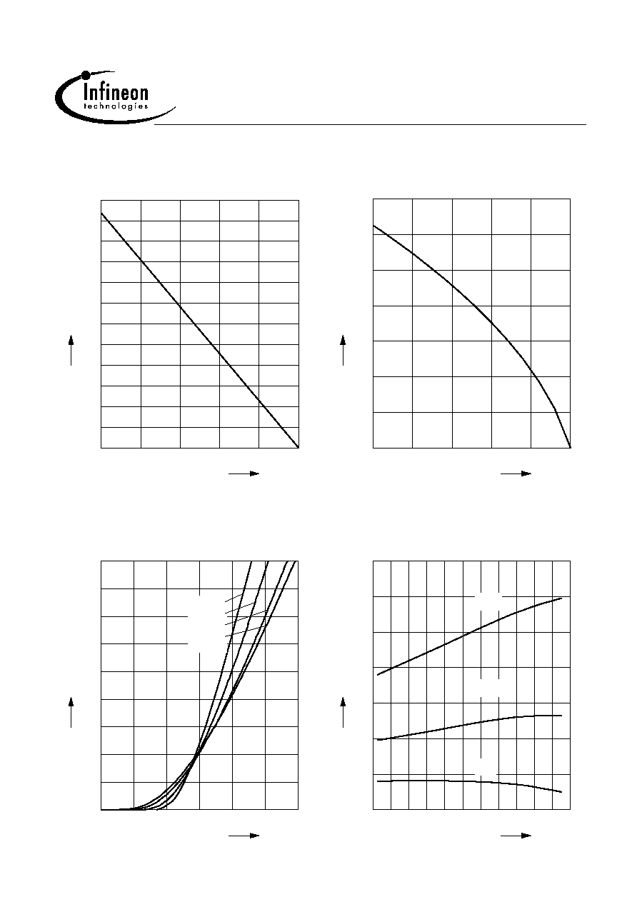
2 Diode forward current
I
F
= f(T
C
)
parameter: T
j
150∞C
25
50
75
100
∞C
150
T
C
0
5
10
15
20
25
A
35
I
F
1 Power dissipation
P
tot
= f (T
C
)
parameter: Tj 150∞C
25
50
75
100
∞C
150
T
C
0
10
20
30
40
50
60
70
80
90
100
W
120
P
tot
3 Typ. diode forward current
I
F
= f (V
F
)
0
0.5
1
1.5
2
V
3
V
F
0
6
12
18
24
30
36
42
A
54
I
F
-55∞C
25∞C
100∞C
150∞C
4 Typ. diode forward voltage
V
F
= f (T
j
)
-60
-20
20
60
100
∞C
160
T
j
1.2
1.4
1.6
1.8
2
2.2
V
2.6
V
F
36A
18A
9A
2003-07-31
Rev.2
Page 5
IDP18E120
IDB18E120
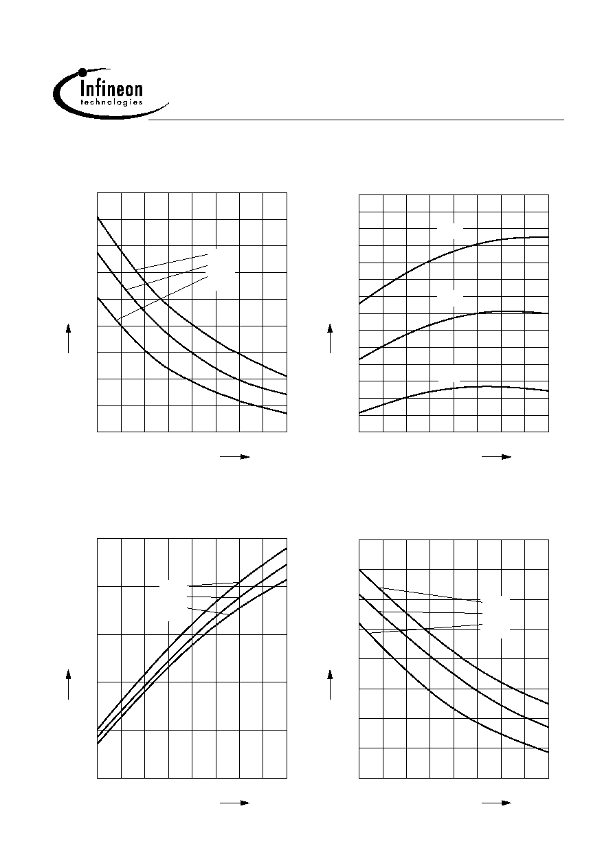
5 Typ. reverse recovery time
t
rr
= f (di
F
/dt)
parameter: V
R
= 800V, T
j
= 125∞C
200
300
400
500
600
700
800
A/µs
1000
di
F
/dt
100
200
300
400
500
600
700
800
ns
1000
t
rr
36A
18A
9A
6 Typ. reverse recovery charge
Q
rr
=f(di
F
/dt)
parameter: V
R
= 800V, T
j
= 125 ∞C
200
300
400
500
600
700
800
A/µs
1000
di
F
/dt
1800
2000
2200
2400
2600
2800
3000
3200
3400
3600
3800
4000
4200
nC
4600
Q
rr
36A
9A
18A
7 Typ. reverse recovery current
I
rr
= f (di
F
/dt)
parameter: V
R
= 800V, T
j
= 125∞C
200
300
400
500
600
700
800
A/µs
1000
di
F
/dt
5
10
15
20
A
30
I
rr
36A
18A
9A
8 Typ. reverse recovery softness factor
S = f(di
F
/dt)
parameter: V
R
= 800V, T
j
= 125∞C
200
300
400
500
600
700
800
A/µs
1000
di
F
/dt
2
4
6
8
10
12
14
18
S
36A
18A
9A
2003-07-31
Rev.2
Page 6
IDP18E120
IDB18E120
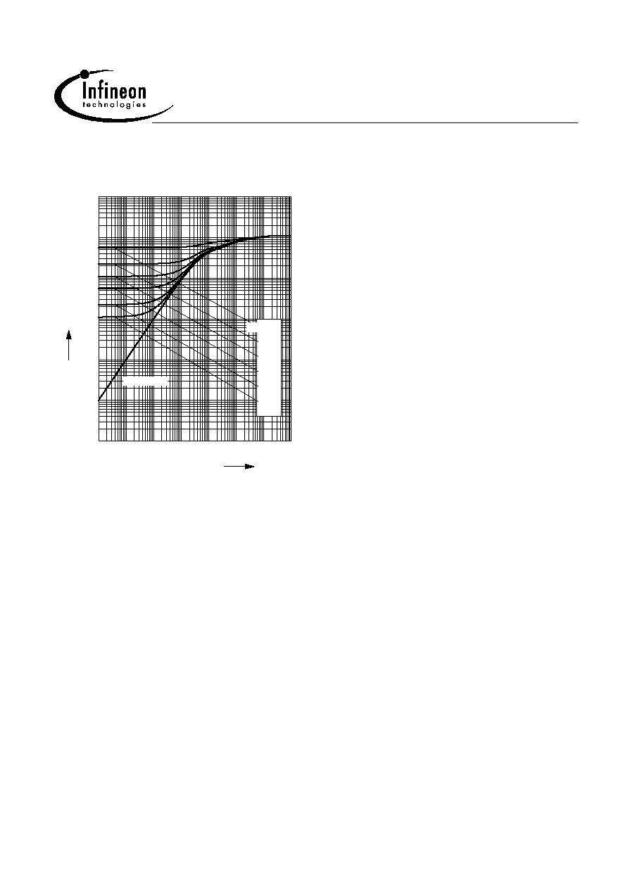
9 Max. transient thermal impedance
Z
thJC
= f (t
p
)
parameter : D = t
p
/T
10
-7
10
-6
10
-5
10
-4
10
-3
10
-2
10
0
s
t
p
-5
10
-4
10
-3
10
-2
10
-1
10
0
10
1
10
K/W
IDP18E120
Z
thJ
C
single pulse
0.01
0.02
0.05
0.10
0.20
D = 0.50
2003-07-31
Rev.2
Page 7
IDP18E120
IDB18E120
TO-220-2-2
symbol
[mm]
[inch]
min
max
min
max
A
9.70
10.10
0.3819
0.3976
B
15.30
15.90
0.6024
0.6260
C
0.65
0.85
0.0256
0.0335
D
3.55
3.85
0.1398
0.1516
E
2.60
3.00
0.1024
0.1181
F
9.00
9.40
0.3543
0.3701
G
13.00
14.00
0.5118
0.5512
H
17.20
17.80
0.6772
0.7008
J
4.40
4.80
0.1732
0.1890
K
0.40
0.60
0.0157
0.0236
L
M
N
P
1.10
1.40
0.0433
0.0551
T
U
V
W
X
0.00
0.40
0.0000
0.0157
0.26 typ.
6.6 typ.
0.51 typ.
13.0 typ.
7.5 typ.
0.295 typ.
2.4 typ.
0.095 typ.
4.4 typ.
0.173 typ.
2.54 typ.
0.1 typ.
dimensions
0.41 typ.
1.05 typ.
A
U
V
W
G
M
T
J
F
L
X
P
D
C
K
N
B
H
E
2003-07-31
Rev.2
Page 8
IDP18E120
IDB18E120
symbol
[mm]
[inch]
min
max
min
max
A
9.80
10.00
0.3858
0.3937
B
C
1.25
1.75
0.0492
0.0689
D
0.95
1.15
0.0374
0.0453
E
F
0.72
0.85
0.0283
0.0335
G
H
4.30
4.50
0.1693
0.1772
K
1.28
1.40
0.0504
0.0551
L
9.00
9.40
0.3543
0.3701
M
2.30
2.50
0.0906
0.0984
N
P
0.00
0.20
0.0000
0.0079
Q
3.30
3.90
0.1299
0.1535
R
S
1.70
2.50
0.0669
0.0984
T
0.50
0.65
0.0197
0.0256
U
V
W
X
Y
Z
9.40 typ.
0.3701 typ.
16.15 typ.
0.6358 typ.
6.43 typ.
0.2532 typ.
4.60 typ.
0.1811 typ.
10.8 typ.
0.4252 typ.
1.35 typ.
0.0532 typ.
14.1 typ.
0.5551 typ.
8∞ max
8∞ max
dimensions
2.54 typ.
0.1 typ.
5.08 typ.
0.2 typ.
1.3 typ.
0.0512 typ.
TO-220-3-45 (P-TO220SMD)

2003-07-31
Rev.2
Page 9
IDP18E120
IDB18E120
Published by
Infineon Technologies AG,
Bereichs Kommunikation
St.-Martin-Strasse 53,
D-81541 M¸nchen
© Infineon Technologies AG 1999
All Rights Reserved.
Attention please!
The information herein is given to describe certain components and shall not be considered as warranted
characteristics.
Terms of delivery and rights to technical change reserved.
We hereby disclaim any and all warranties, including but not limited to warranties of non-infringement,
regarding circuits, descriptions and charts stated herein.
Infineon Technologies is an approved CECC manufacturer.
Information
For further information on technology, delivery terms and conditions and prices please contact your nearest
Infineon Technologies Office in Germany or our Infineon Technologies Reprensatives worldwide (see address list).
Warnings
Due to technical requirements components may contain dangerous substances.
For information on the types in question please contact your nearest Infineon Technologies Office.
Infineon Technologies Components may only be used in life-support devices or systems with the express
written approval of Infineon Technologies, if a failure of such components can reasonably be expected to
cause the failure of that life-support device or system, or to affect the safety or effectiveness of that device
or system Life support devices or systems are intended to be implanted in the human body, or to support
and/or maintain and sustain and/or protect human life. If they fail, it is reasonable to assume that the health
of the user or other persons may be endangered.