Data Book
1
03.00
GaAs HEMT
CFH 77
Target Data Sheet
∑
Very low noise
∑
Very high gain
∑
For low noise front end amplifiers up to 20 GHz
∑
For DBS down converters
ESD: Electrostatic discharge sensitive device, ob-
serve handling precautions!
Type
Marking
Ordering Code
(taped)
Package
1)
1)
Dimensions see Page 5.
CFH 77
t.b.d.
Q62702-G117
MW-4
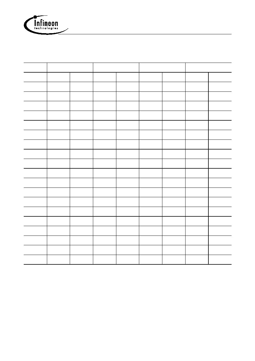
Maximum Ratings
Symbol
Value
Unit
Drain-source voltage
V
DS
3.5
V
Drain-gate voltage
V
DG
4.5
V
Gate-source voltage
V
GS
≠ 3.0
V
Drain current
I
D
60
mA
Channel temperature
T
Ch
150
∞
C
Storage temperature range
T
stg
≠ 65 ... + 150
∞
C
Total power dissipation (
T
S
51
∞
C)
1)
1)
T
S
: Temperature measured at soldering point.
P
tot
180
mW
Thermal Resistance
Symbol
Value
Unit
Channel-soldering point source
R
thChS
550
K/W
MW-4
CFH 77
Data Book
2
03.00
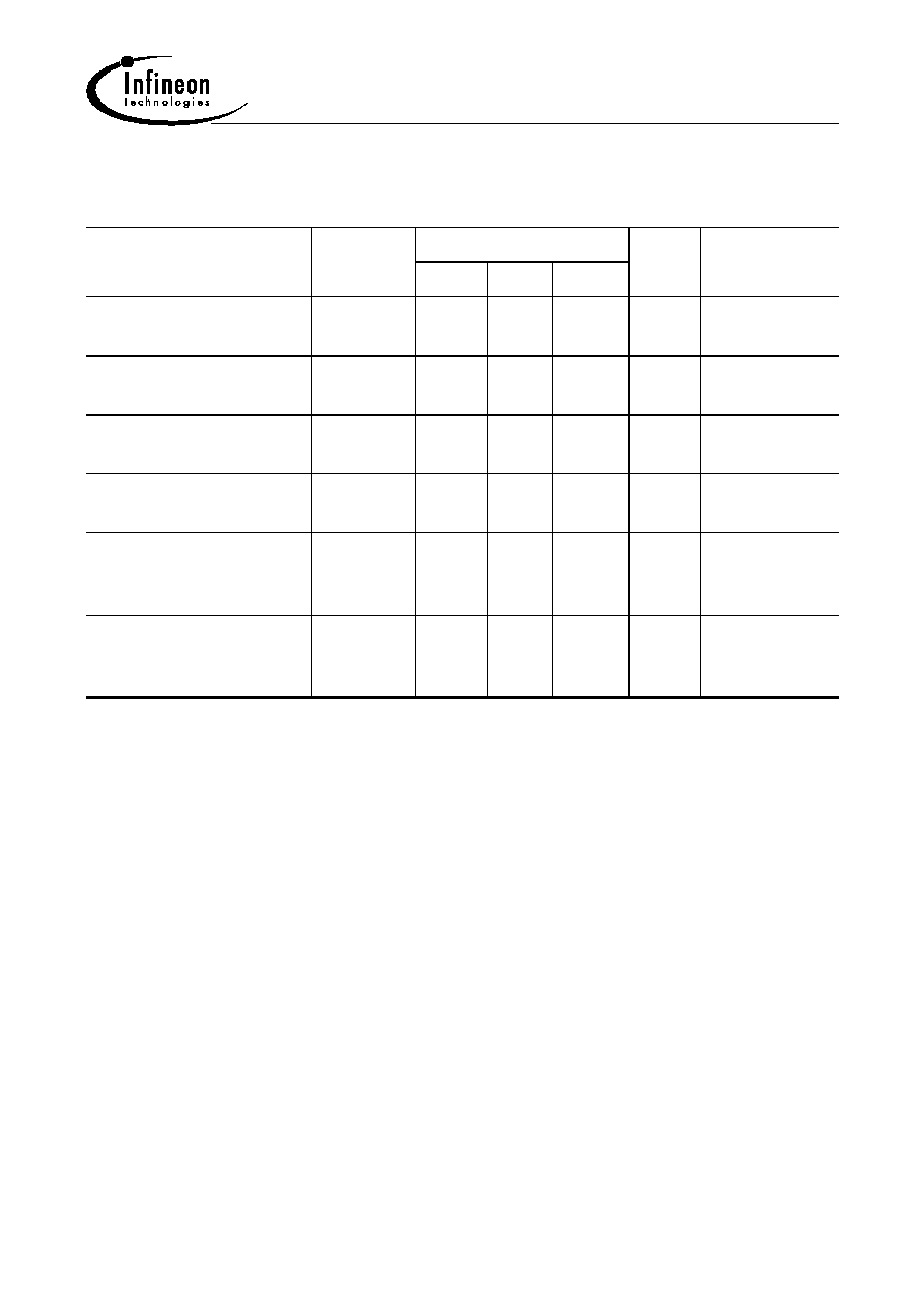
Electrical Characteristics
T
A
= 25
∞
C, unless otherwise specified
Characteristics
Symbol
Limit Values
Unit
Test
Conditions
min.
typ.
max.
Drain-source saturation
current
I
DSS
15
30
60
mA
V
DS
= 2 V
V
GS
= 0 V
Pinch-off voltage
V
GS(P)
≠ 2
≠ 0.7
≠ 0.2
V
V
DS
= 2 V
I
D
= 1 mA
Gate leakage current
I
G
≠
0.05
2
µ
A
V
DS
= 2 V
I
D
= 15 mA
Transconductance
g
m
50
65
≠
mS
V
DS
= 2 V
I
D
= 15 mA
Noise figure
F
≠
0.7
≠
dB
V
DS
= 2 V
I
D
= 15 mA
f
= 12 GHz
Associated gain
G
a
≠
10.5
≠
dB
V
DS
= 2 V
I
D
= 15 mA
f
= 12 GHz
CFH 77
Data Book
5
03.00
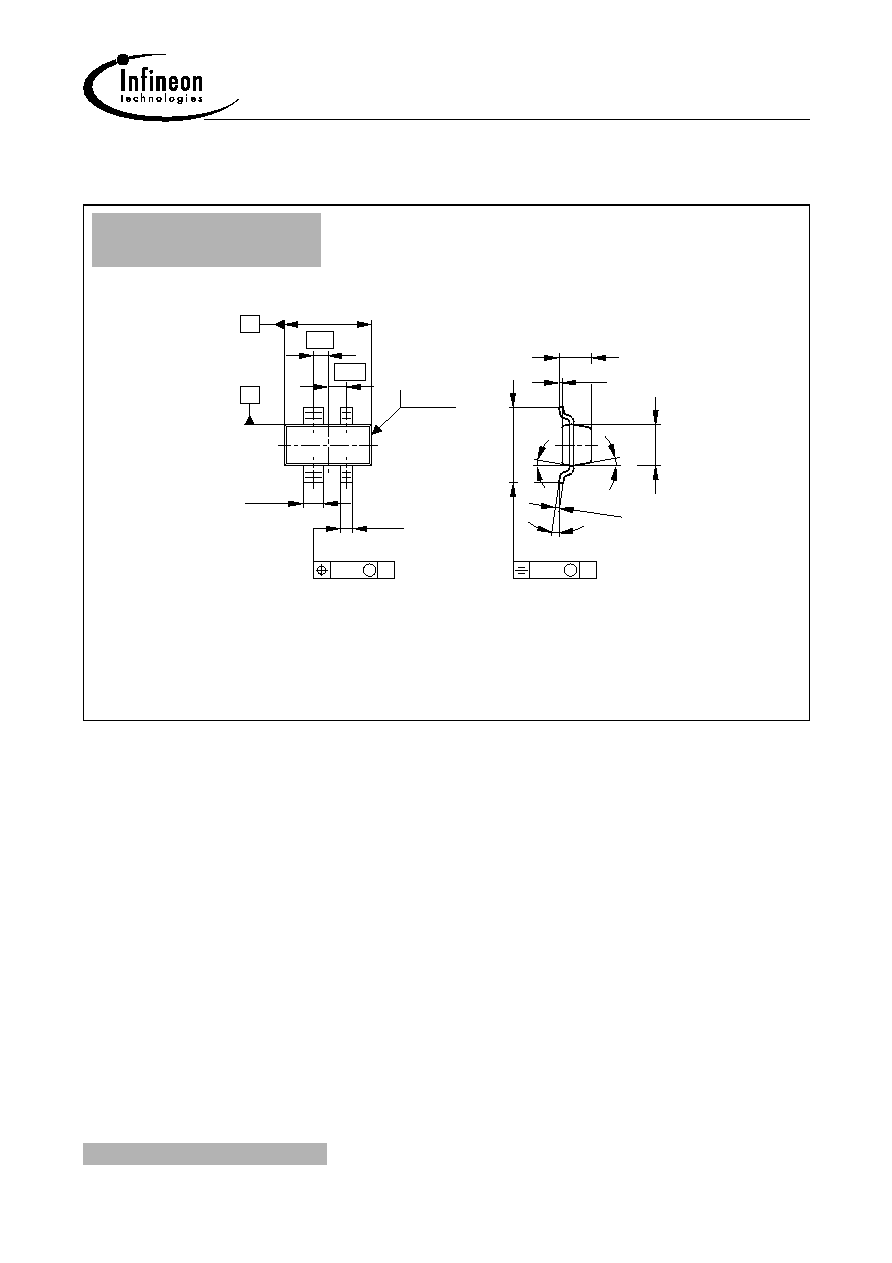
Package Outlines
0.7
-0.05
1
1.1 max
2∞... 30∞
2.6
max
10∞max
10∞max
0.1 max
2.9
±0.1
1.3
±0.1
2
3
4
B
M
0.25
A
B
+0.1
+0.1
-0.05
0.4
GSO05553
acc. to
+0.2
DIN 6784
0.65
0.5
0.08...0.15
A
M
0.20
MW-4
(Special Package)
Pin assignment:
1 = Source
2 = Drain
3 = Source
4 = Gate
Sorts of Packing
Package outlines for tubes, trays etc. are contained in
our Data Book "Package Information".
Dimensions in mm
SMD = Surface Mounted Device