
Data Sheet
1
2001-01-01
GaAs MMIC
CMY 213
Data Sheet
∑
Ultralinear mixer with integrated IF-amplifier and
LO-Buffer for CDMA receiver applications
∑
Typical overall performance at cellular frequen-
cies for
P
LO
= ≠ 5 dBm (operation conditions: 3 V,
8 mA;
f
RF
= 850 MHz;
f
LO
= 740 MHz):
Gain 9.5 dB, Input IP3 10 dBm, Noise figure 8 dB
∑
RF-frequency range 0.5 - 2.5 GHz
∑
Operating voltage range: 2.6 to 5 V
∑
Small SCT-598-8-1 plastic package
ESD: Electrostatic discharge sensitive device,
observe handling precautions!
Type
Marking
Ordering Code
(tape and reel)
Package
CMY 213
M6s
Q62702-M0032
SCT-598-8-1
Maximum Ratings
Parameter
Port
Symbol
Limit Values
Unit
min.
max.
Supply Voltage
3, 6
V
DD
0
5
V
DC-Voltage at LO Input
4
V
6
≠ 3
0.5
V
DC-Voltage at Mixer RF-IF Port
1
V
8
≠ 0.5
+ 0.5
V
Power into Mixer RF Port
1
P
RF
≠
10
dBm
Power into LO Input
4
P
IN, LO
≠ 10
10
dBm
Channel Temperature
≠
T
Ch
≠
150
∞
C
Operating Temperature
≠
T
OP
≠ 30
85
∞
C
Storage Temperature
≠
T
stg
≠ 55
150
∞
C
VPW05982
7
5
2
3
1
4
6
8

GaAs Components
CMY 213
Data Sheet
2
2001-01-01
Figure 1
Block Diagram
Thermal Resistance
Parameter
Symbol
Values
Unit
Channel to Soldering Point (GND)
R
thChS
260
K/W
Electrical Characteristics - Mixer
Parameter
Comment
Limit Values
Unit
min.
typ.
max.
RF - Frequency range
External match
0.5
≠
2.5
GHz
LO - Frequency range
External match
0.5
≠
2.5
GHz
IF Frequency range
External match
45
≠
250
MHz
EHT09240
4
5
CMY 213
3
1
2
6
7
8
RF IN
Mixer
GND
Mixer
DD
V
Mixer
LO IN
Source
IF AMP
IF AMP
OUT
GND
IN
IF AMP
IF OUT

GaAs Components
CMY 213
Data Sheet
3
2001-01-01
*Important Note:
During production, the RF performance at PCS frequencies is screened. The passed
devices also achieve the specified RF performance at cellular frequencies.
Typical Performance at Cellular Frequencies*
T
A
= 25
∞
C;
V
DD
= 3 V,
f
RF
= 850 MHz;
f
LO
= 740 MHz;
P
LO
= ≠ 5 dBm;
f
IF
= 110 MHz;
Z
S
=
Z
L
= 50
; unless otherwise specified
Parameter
Symbol
Limit Values
Unit
min.
typ.
max.
Total operating Current
(Mixer + IF amplifier)
I
OP
≠
8.0
9.5
mA
Conversion Gain
G
C
8.0
9.5
≠
dB
SSB Noise Figure
F
SSB
≠
8
≠
dB
RF Input -/ IF Output return loss
(external matching required)
RFIrl/IFOrl
≠
10
≠
dB
3
rd
Order Input Intercept Point
IIP3
8
10
≠
dBm
LO-RF Isolation
Iso
≠
10
≠
dB
Test Conditions at PCS Frequencies
T
A
= 25
∞
C;
V
DD
= 3 V,
f
RF
= 1960 MHz;
f
LO
= 1750 MHz;
P
LO
= ≠ 5 dBm;
f
IF
= 210 MHz;
Z
S
=
Z
L
= 50
; unless otherwise specified
Parameter
Symbol
Limit Values
Unit
min.
typ.
max.
Total operating Current
(Mixer + IF amplifier)
I
OP
≠
8.0
9.5
mA
Conversion Gain
G
C
7
8.5
≠
dB
SSB Noise Figure
F
SSB
≠
8.5
≠
dB
RF Input -/ IF Output return loss
(external matching required)
RFIrl/IFOrl
≠
10
≠
dB
3
rd
Order Input Intercept Point
IIP3
10
12
≠
dBm
LO-RF Isolation
Iso
≠
6
≠
dB
Data Sheet
4
2001-01-01
GaAs Components
CMY 213
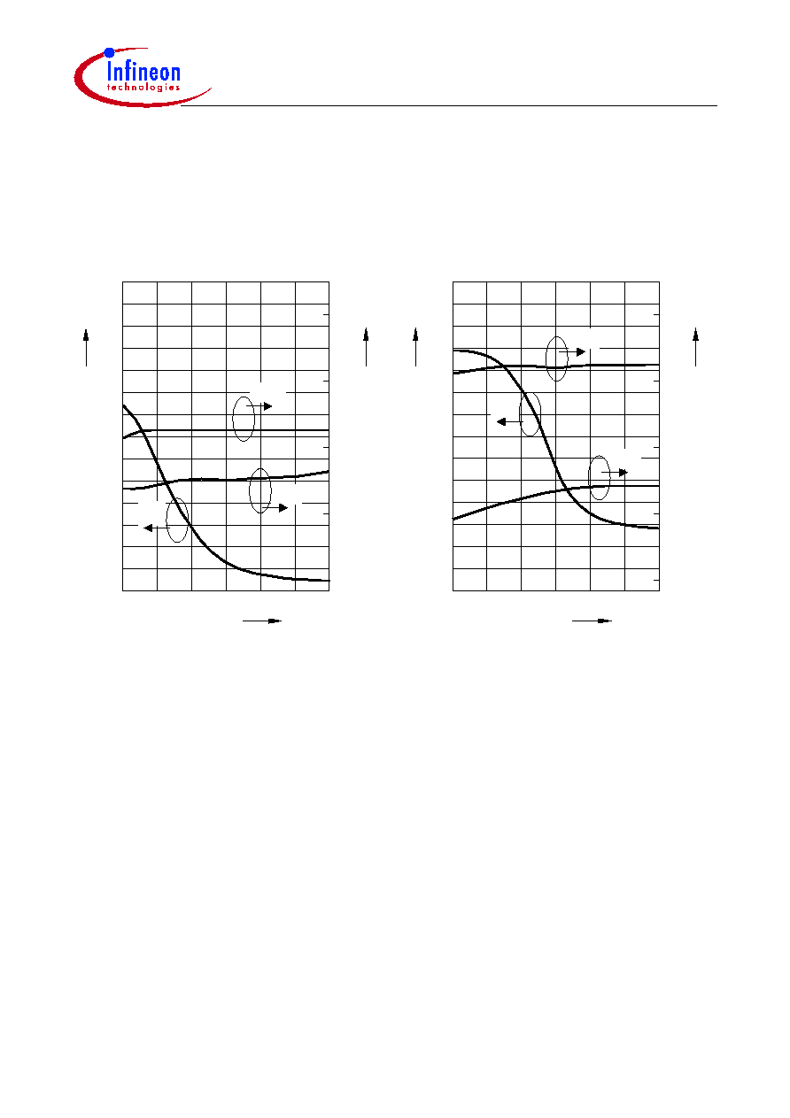
Typical Device Behavior at Cellular
Frequencies
T
A
= 25
∞
C;
V
DD
= 3 V,
f
RF
= 850 MHz;
f
LO
= 740 MHz;
f
IF
= 110 MHz;
Z
S
=
Z
L
= 50
; unless otherwise specified
-12
6
EHT09241
6
dBm
Gain, IIP3
Operating Current
LO Power
-10
-8
-6
-4
0
dB, dBm
8
10
12
14
16
18
20
mA
8
10
12
14
7
9
11
13
15
Gain
IIP3
OP
I
Typical Device Behavior at PCS
Frequencies
T
A
= 25
∞
C;
V
DD
= 3 V,
f
RF
= 1960 MHz;
f
LO
= 1750 MHz;
f
IF
= 210 MHz;
Z
S
=
Z
L
= 50
; unless otherwise specified
-12
6
EHT09242
6
dBm
Gain, IIP3
Operating Current
LO Power
-10
-8
-6
-4
0
dB, dBm
8
10
12
14
16
18
20
mA
8
10
12
14
7
9
11
13
15
IIP3
Gain
OP
I

GaAs Components
CMY 213
Data Sheet
5
2001-01-01
Figure 2
Test Circuit
EHT09227
Mixer
4
5
3
2
1
7
6
8
RF Input
Ext1
L
C
Ext1
RF
Ext5
C
+3 V
GND
L
Ext5
D
V
LO
Ext4
Ext4
C
L
Input
Input
Ext7
C
LO Input
Ext5
C
GND
S Cap
V
Ext2
C
L
Ext2
IF Input
Ext6
C
IF
Output
+3 V
Ext3
L
C
Ext3
IF Output
IF
Buffer