2002-01-17
Page 1
IPD09N03L
Opti
MOS
®
Buck converter series
Product Summary
V
DS
30
V
R
DS(on)
8.9
m
I
D
30
A
Feature
·
N-Channel
·
Logic Level
·
Low On-Resistance R
DS(on)
·
Excellent Gate Charge x R
DS(on)
product (FOM)
·
Superior thermal resistance
·
175°C operating temperature
·
Avalanche rated
·
dv/dt rated
·
Ideal for fast switching buck converter
P- TO252 -3-11
Marking
09N03L
Type
Package
Ordering Code
IPD09N03L
P- TO252 -3-11 Q67042-S4110
Maximum Ratings, at T
j
= 25 °C, unless otherwise specified
Parameter
Symbol
Value
Unit
Continuous drain current
1)
T
C
=25°C
T
C
=100°C
I
D
30
30
A
Pulsed drain current
T
C
=25°C
I
D puls
120
Avalanche energy, single pulse
I
D
=30A, V
DD
=25V, R
GS
=25
E
AS
150
mJ
Repetitive avalanche energy, limited by T
jmax
2)
E
AR
10
Reverse diode dv/dt
I
S
=30A, V
DS
=24V, di/dt=200A/µs, T
jmax
=175°C
dv/dt
6
kV/µs
Gate source voltage
V
GS
±20
V
Power dissipation
T
C
=25°C
P
tot
100
W
Operating and storage temperature
T
j ,
T
stg
-55... +175
°C
IEC climatic category; DIN IEC 68-1
55/175/56
2002-01-17
Page 2
IPD09N03L
Thermal Characteristics
Parameter
Symbol
Values
Unit
min.
typ.
max.
Characteristics
Thermal resistance, junction - case
R
thJC
-
1
1.5
K/W
Thermal resistance, junction - ambient, leaded
R
thJA
-
-
100
SMD version, device on PCB:
@ min. footprint
@ 6 cm
2
cooling area
3)
R
thJA
-
-
-
-
75
50
Electrical Characteristics, at T
j
= 25 °C, unless otherwise specified
Parameter
Symbol
Values
Unit
min.
typ.
max.
Static Characteristics
Drain-source breakdown voltage
V
GS
=0V, I
D
=1mA
V
(BR)DSS
30
-
-
V
Gate threshold voltage, V
GS
= V
DS
I
D
= 50 µA
V
GS(th)
1.2
1.6
2
Zero gate voltage drain current
V
DS
=30V, V
GS
=0V, T
j
=25°C
V
DS
=30V, V
GS
=0V, T
j
=125°C
I
DSS
-
-
0.01
10
1
100
µA
Gate-source leakage current
V
GS
=20V, V
DS
=0V
I
GSS
-
1
100
nA
Drain-source on-state resistance
V
GS
=4.5V, I
D
=30A
R
DS(on)
-
10.6
13.6 m
Drain-source on-state resistance
V
GS
=10V, I
D
=30A
R
DS(on)
-
7.2
8.9
1Current limited by bondwire ; with an R
thJC
= 1.5K/W the chip is able to carry I
D
= 83A at 25°C, for detailed
information see app.-note ANPS071E available at www.infineon.com/optimos
2Defined by design. Not subject to production test.
3Device on 40mm*40mm*1.5mm epoxy PCB FR4 with 6cm² (one layer, 70 µm thick) copper area for drain
connection. PCB is vertical without blown air.
2002-01-17
Page 3
IPD09N03L
Electrical Characteristics
Parameter
Symbol
Conditions
Values
Unit
min.
typ.
max.
Dynamic Characteristics
Transconductance
g
fs
V
DS
2*I
D
*R
DS(on)max
,
I
D
=30A
23.8
47.5
-
S
Input capacitance
C
iss
V
GS
=0V, V
DS
=25V,
f=1MHz
-
1160 1550 pF
Output capacitance
C
oss
-
450
600
Reverse transfer capacitance
C
rss
-
120
175
Gate resistance
R
G
-
1.5
-
Turn-on delay time
t
d(on)
V
DD
=15V, V
GS
=10V,
I
D
=15A,
R
G
=5.4
-
7.4
11.1 ns
Rise time
t
r
13
20
Turn-off delay time
t
d(off)
-
28.4
42.6
Fall time
t
f
-
7.6
11.4
Gate Charge Characteristics
Gate to source charge
Q
gs
V
DD
=15V, I
D
=15A
-
3
4
nC
Gate to drain charge
Q
gd
-
9.2
12.5
Gate charge total
Q
g
V
DD
=15V, I
D
=15A,
V
GS
=0 to 5V
-
18.2
24.2
Output charge
Q
oss
V
DS
=15V, I
D
=15A,
V
GS
=0V
-
16.5
21.9 nC
Gate plateau voltage
V
(plateau) V
DD
=15V, I
D
=15A
-
2.7
-
V
Reverse Diode
Inverse diode continuous
forward current
I
S
T
C
=25°C
-
-
30
A
Inv. diode direct current, pulsed
I
SM
-
-
120
Inverse diode forward voltage
V
SD
V
GS
=0V, I
F
=30A
-
0.9
1.2
V
Reverse recovery time
t
rr
V
R
=-V, I
F=
l
S
,
di
F
/dt=100A/µs
-
31
39
ns
Reverse recovery charge
Q
rr
-
29
37
nC
2002-01-17
Page 5
IPD09N03L
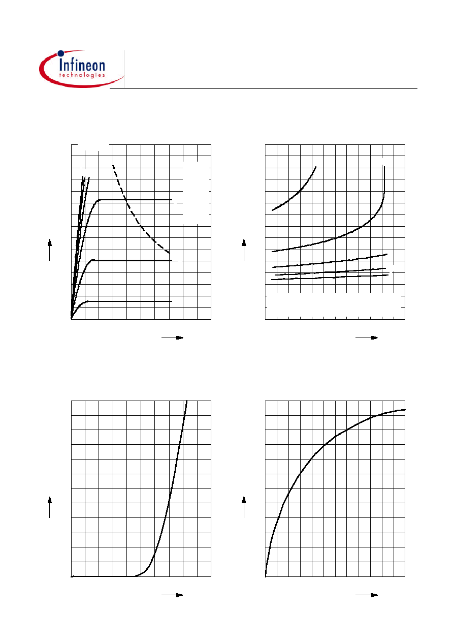
5 Typ. output characteristic
I
D
= f (V
DS
); T
j
=25°C
parameter: t
p
= 80 µs
0
0.5
1
1.5
2
2.5
3
3.5
4
V
5
V
DS
0
5
10
15
20
25
30
35
40
45
50
55
60
A
75
IPD09N03L
I
D
VGS [V]
a
a
3.0
b
b
3.5
c
c
4.0
d
d
4.5
e
e
5.0
f
P
tot
= 100W
f
5.5
6 Typ. drain-source on resistance
R
DS(on)
= f (I
D
)
parameter: V
GS
0
10
20
30
40
A
60
I
D
0
2
4
6
8
10
12
14
16
18
20
22
24
m
30
IPD09N03L
R
DS(on)
V
GS
[V] =
b
b
3.5
c
c
4.0
d
d
4.5
e
e
5.0
f
f
5.5
7 Typ. transfer characteristics
I
D
= f ( V
GS
); V
DS
2 x I
D
x R
DS(on)max
parameter: t
p
= 80 µs
0
0.5
1
1.5
2
2.5
3
3.5
4
V
5
V
GS
0
5
10
15
20
25
30
35
40
45
50
A
60
I
D
8 Typ. forward transconductance
g
fs
= f(I
D
); T
j
=25°C
parameter: g
fs
0
10
20
30
40
A
60
I
D
0
5
10
15
20
25
30
35
40
45
50
S
60
g
fs