2003-05-09
Page 1
SPP80N06S2-09
SPB80N06S2-09
Opti
MOS
Æ
Power-Transistor
Product Summary
V
DS
55
V
R
DS(on)
9.1
m
I
D
80
A
Feature
∑
N-Channel
∑
Enhancement mode
∑
175∞C operating temperature
∑
Avalanche rated
∑
dv/dt rated
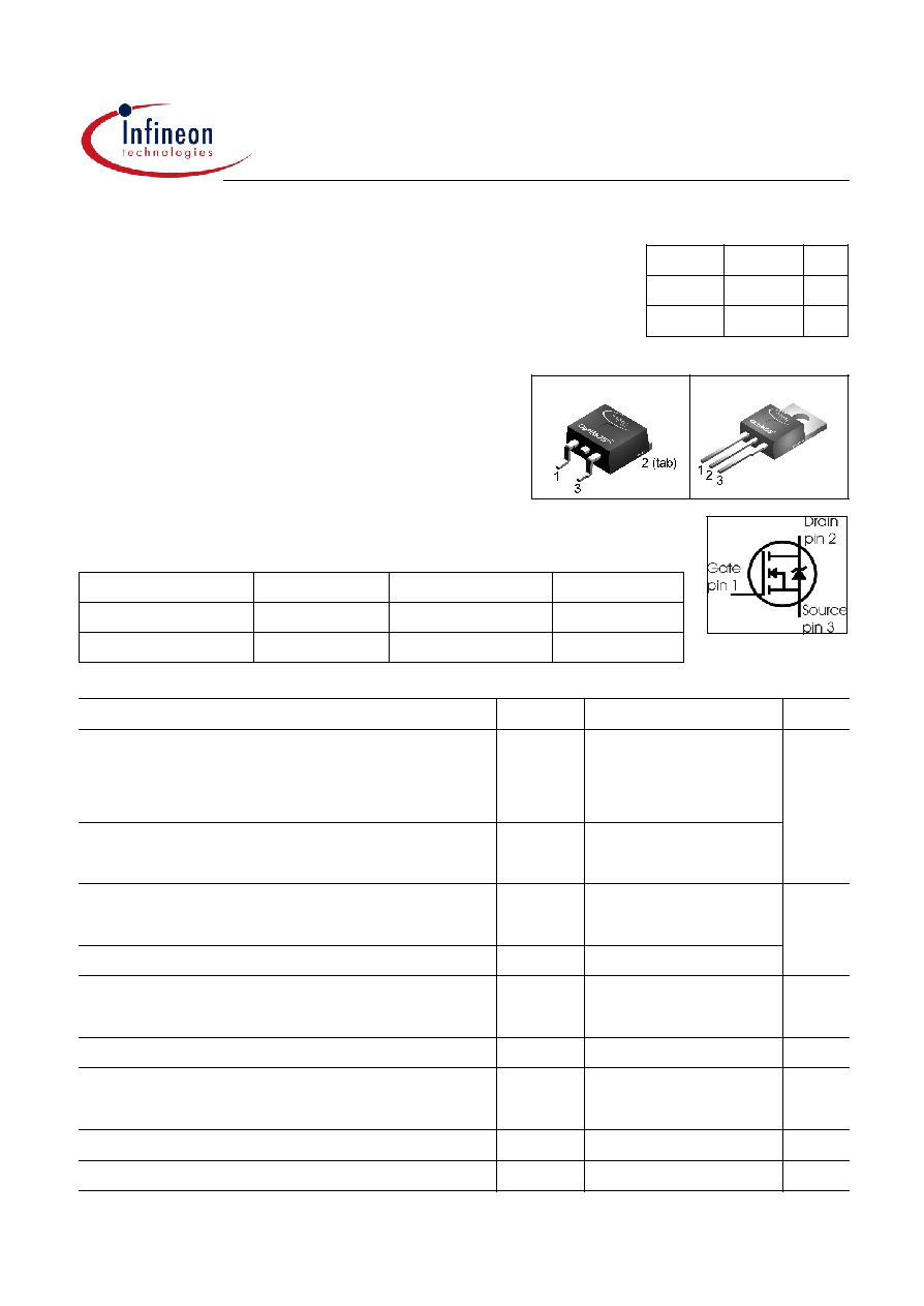
P- TO263 -3-2
P- TO220 -3-1
Marking
2N0609
2N0609
Type
Package
Ordering Code
SPP80N06S2-09
P- TO220 -3-1 Q67060-S6025
SPB80N06S2-09
P- TO263 -3-2 Q67060-S6027
Maximum Ratings, at
T
j
= 25 ∞C, unless otherwise specified
Parameter
Symbol
Value
Unit
Continuous drain current
1)
T
C
=25∞C
I
D
80
70
A
Pulsed drain current
T
C
=25∞C
I
D puls
320
Avalanche energy, single pulse
I
D
=80 A ,
V
DD
=25V,
R
GS
=25
E
AS
370
mJ
Repetitive avalanche energy, limited by T
jmax
2)
E
AR
19
Reverse diode dv/dt
I
S
=80A,
V
DS
=44V,
di/dt=200A/µs, T
jmax
=175∞C
dv/dt
6
kV/µs
Gate source voltage
V
GS
±20
V
Power dissipation
T
C
=25∞C
P
tot
190
W
Operating and storage temperature
T
j ,
T
stg
-55... +175
∞C
IEC climatic category; DIN IEC 68-1
55/175/56
2003-05-09
Page 2
SPP80N06S2-09
SPB80N06S2-09
Thermal Characteristics
Parameter
Symbol
Values
Unit
min.
typ.
max.
Characteristics
Thermal resistance, junction - case
R
thJC
-
0.52
0.8
K/W
Thermal resistance, junction - ambient, leaded
R
thJA
-
-
62
SMD version, device on PCB:
@ min. footprint
@ 6 cm
2
cooling area
3)
R
thJA
-
-
-
-
62
40
Electrical Characteristics, at
T
j
= 25 ∞C, unless otherwise specified
Parameter
Symbol
Values
Unit
min.
typ.
max.
Static Characteristics
Drain-source breakdown voltage
V
GS
=0V, I
D
=1mA
V
(BR)DSS
55
-
-
V
Gate threshold voltage,
V
GS
=
V
DS
I
D
= 125 µA
V
GS(th)
2.1
3
4
Zero gate voltage drain current
V
DS
=55V,
V
GS
=0V,
T
j
=25∞C
V
DS
=55V,
V
GS
=0V,
T
j
=125∞C
I
DSS
-
-
0.01
1
1
100
µA
Gate-source leakage current
V
GS
=20V,
V
DS
=0V
I
GSS
-
1
100
nA
Drain-source on-state resistance
V
GS
=10V, I
D
=50A
R
DS(on)
-
7.6
9.1
m
1Current limited by bondwire ; with an R
thJC
= 0.8K/W the chip is able to carry I
D
= 99A at 25∞C, for detailed
information see app.-note ANPS071E available at www.infineon.com/optimos
2Defined by design. Not subject to production test.
3Device on 40mm*40mm*1.5mm epoxy PCB FR4 with 6cm≤ (one layer, 70 µm thick) copper area for drain
connection. PCB is vertical without blown air.
2003-05-09
Page 3
SPP80N06S2-09
SPB80N06S2-09
Electrical Characteristics
Parameter
Symbol
Conditions
Values
Unit
min.
typ.
max.
Dynamic Characteristics
Transconductance
g
fs
V
DS
2*I
D
*R
DS(on)max
,
I
D
=70A
34
68
-
S
Input capacitance
C
iss
V
GS
=0V,
V
DS
=25V,
f=1MHz
-
2360 3140 pF
Output capacitance
C
oss
-
610
810
Reverse transfer capacitance
C
rss
-
150
230
Turn-on delay time
t
d(on)
V
DD
=30V,
V
GS
=10V,
I
D
=80A,
R
G
=4.7
-
14
21
ns
Rise time
t
r
-
29
44
Turn-off delay time
t
d(off)
-
39
58
Fall time
t
f
-
28
42
Gate Charge Characteristics
Gate to source charge
Q
gs
V
DD
=44V, I
D
=80A
-
12
16
nC
Gate to drain charge
Q
gd
-
24
37
Gate charge total
Q
g
V
DD
=44V, I
D
=80A,
V
GS
=0 to 10V
-
60
80
Gate plateau voltage
V
(plateau) V
DD
=44V, I
D
=80A
-
5.8
-
V
Reverse Diode
Inverse diode continuous
forward current
I
S
T
C
=25∞C
-
-
80
A
Inv. diode direct current, pulsed
I
SM
-
-
320
Inverse diode forward voltage
V
SD
V
GS
=0V,
I
F
=80A
-
0.9
1.3
V
Reverse recovery time
t
rr
V
R
=30V,
I
F=
l
S
,
di
F
/dt=100A/µs
-
50
63
ns
Reverse recovery charge
Q
rr
-
76
95
nC
2003-05-09
Page 4
SPP80N06S2-09
SPB80N06S2-09
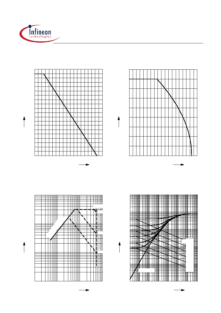
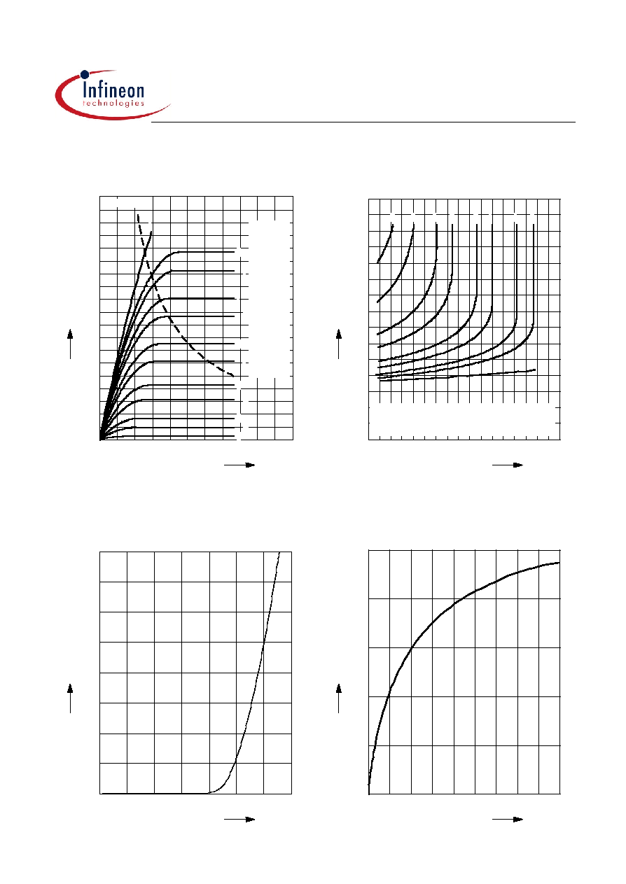
1 Power dissipation
P
tot
= f (
T
C
)
parameter: V
GS
6 V
0
20
40
60
80 100 120 140 160
∞C
190
T
C
0
20
40
60
80
100
120
140
160
W
200
SPP80N06S2-09
P
tot
2 Drain current
I
D
= f (
T
C
)
parameter: V
GS
10 V
0
20
40
60
80 100 120 140 160
∞C
190
T
C
0
10
20
30
40
50
60
70
A
90
SPP80N06S2-09
I
D
4 Max. transient thermal impedance
Z
thJC
= f (t
p
)
parameter : D = t
p
/T
10
-7
10
-6
10
-5
10
-4
10
-3
10
-2
10
0
s
t
p
-4
10
-3
10
-2
10
-1
10
0
10
1
10
K/W
SPP80N06S2-09
Z
thJC
single pulse
0.01
0.02
0.05
0.10
0.20
D = 0.50
3 Safe operating area
I
D
= f ( V
DS
)
parameter : D = 0 ,
T
C
= 25 ∞C
10
-1
10
0
10
1
10
2
V
V
DS
0
10
1
10
2
10
3
10
A
SPP80N06S2-09
I
D
R
DS(on)
=
V
DS
/
I
D
1 ms
100 µs
10 µs
t
p = 7.3µs
2003-05-09
Page 5
SPP80N06S2-09
SPB80N06S2-09
5 Typ. output characteristic
I
D
= f (
V
DS
);
T
j
=25∞C
parameter: t
p
= 80 µs
0
1
2
3
4
V
5.5
V
DS
0
20
40
60
80
100
120
140
160
A
190
SPP80N06S2-09
I
D
VGS [V]
a
a
4.5
b
b
4.8
c
c
5.0
d
d
5.3
e
e
5.5
f
f
5.8
g
g
6.0
h
h
6.3
i
i
6.5
j
j
6.8
k
k
7.0
l
P
tot
= 190W
l
10.0
6 Typ. drain-source on resistance
R
DS(on)
= f (I
D
)
parameter:
V
GS
0
20
40
60
80
100 120 140
A
170
I
D
0
2
4
6
8
10
12
14
16
18
20
22
24
30
SPP80N06S2-09
R
DS(on)
V
GS
[V] =
d
d
5.3
e
e
5.5
f
f
5.8
g
g
6.0
h
h
6.3
i
i
6.5
j
j
6.8
k
k
7.0
l
l
10.0
7 Typ. transfer characteristics
I
D
= f ( V
GS
); V
DS
2 x I
D
x R
DS(on)max
parameter: t
p
= 80 µs
0
1
2
3
4
5
V
7
V
GS
0
20
40
60
80
100
120
A
160
I
D
8 Typ. forward transconductance
g
fs
= f(I
D
);
T
j
=25∞C
parameter:
g
fs
0
10
20
30
40
50
60
70
A
90
I
D
0
15
30
45
S
75
g
fs
2003-05-09
Page 6
SPP80N06S2-09
SPB80N06S2-09
9 Drain-source on-state resistance
R
DS(on)
= f (T
j
)
parameter : I
D
= 50 A,
V
GS
= 10 V
-60
-20
20
60
100
140 ∞C
200
T
j
0
2
4
6
8
10
12
14
16
18
20
22
24
30
SPP80N06S2-09
R
DS(on)
typ
98%
10 Typ. gate threshold voltage
V
GS(th)
= f (Tj)
parameter: V
GS
= V
DS
-60
-20
20
60
100
∞C
180
T
j
0
0.5
1
1.5
2
2.5
3
V
4
V
GS(th)
125
µ
A
625
µ
A
11 Typ. capacitances
C = f (
V
DS
)
parameter:
V
GS
=0V, f=1 MHz
0
5
10
15
20
V
30
V
DS
2
10
3
10
4
10
pF
C
C
iss
C
oss
C
rss
12 Forward character. of reverse diode
I
F
= f (V
SD
)
parameter: Tj , t
p
= 80 µs
0
0.4
0.8
1.2
1.6
2
2.4
V
3
V
SD
0
10
1
10
2
10
3
10
A
SPP80N06S2-09
I
F
T
j
= 25 ∞C typ
T
j
= 25 ∞C (98%)
T
j
= 175 ∞C typ
T
j
= 175 ∞C (98%)
2003-05-09
Page 7
SPP80N06S2-09
SPB80N06S2-09
13 Typ. avalanche energy
E
AS
= f (
T
j
)
par.: I
D
= 80 A ,
V
DD
= 25 V,
R
GS
= 25
25
45
65
85
105
125
145
∞C
185
T
j
0
40
80
120
160
200
240
280
320
mJ
380
E
AS
14 Typ. gate charge
V
GS
= f (Q
Gate
)
parameter: I
D
= 80 A pulsed
0
10
20
30
40
50
60
70
80
nC
100
Q
Gate
0
2
4
6
8
10
12
V
16
SPP80N06S2-09
V
GS
0,8 V
DS max
DS max
V
0,2
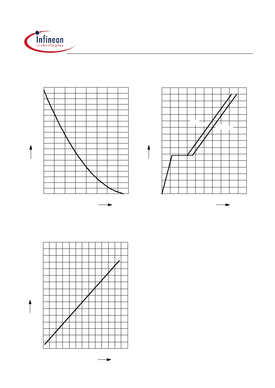
15 Drain-source breakdown voltage
V
(BR)DSS
= f (
T
j
)
parameter: I
D
=10 mA
-60
-20
20
60
100
140
∞C
200
T
j
50
52
54
56
58
60
62
V
66
SPP80N06S2-09
V
(BR)DSS

2003-05-09
Page 8
SPP80N06S2-09
SPB80N06S2-09
Published by
Infineon Technologies AG,
Bereichs Kommunikation
St.-Martin-Strasse 53,
D-81541 M¸nchen
© Infineon Technologies AG 1999
All Rights Reserved.
Attention please!
The information herein is given to describe certain components and shall not be considered as warranted
characteristics.
Terms of delivery and rights to technical change reserved.
We hereby disclaim any and all warranties, including but not limited to warranties of non-infringement,
regarding circuits, descriptions and charts stated herein.
Infineon Technologies is an approved CECC manufacturer.
Information
For further information on technology, delivery terms and conditions and prices please contact your nearest
Infineon Technologies Office in Germany or our Infineon Technologies Reprensatives worldwide (see address list).
Warnings
Due to technical requirements components may contain dangerous substances.
For information on the types in question please contact your nearest Infineon Technologies Office.
Infineon Technologies Components may only be used in life-support devices or systems with the express
written approval of Infineon Technologies, if a failure of such components can reasonably be expected to
cause the failure of that life-support device or system, or to affect the safety or effectiveness of that device
or system Life support devices or systems are intended to be implanted in the human body, or to support
and/or maintain and sustain and/or protect human life. If they fail, it is reasonable to assume that the health
of the user or other persons may be endangered.
Further information
Please notice that the part number is BSPP80N06S2-09 and BSPB80N06S2-09, for simplicity the device is referred
to by the term SPP80N06S2-09 and SPB80N06S2-09 throughout this documentation.