 | ÐлекÑÑоннÑй компоненÑ: TDA16846G | СкаÑаÑÑ:  PDF PDF  ZIP ZIP |
Äîêóìåíòàöèÿ è îïèñàíèÿ www.docs.chipfind.ru

ICs for Consumer Electronics
Controller for Switch Mode Power Supplies Supporting Low Power
Standby and Power Factor Correction
TDA 16846/TDA 16847
Data Sheet 2000-01-14

TDA 16846/TDA 16847
Revision History:
Current Version: 2000-01-14
Previous Version: 1999-07-05
Page
(in previous
Version)
Page
(in current
Version)
Subjects (major changes since last revision)
3
3, 28
P-DSO package added
Edition 01.00
Published by Infineon Technologies AG i. Gr.,
St.-Martin-Strasse 53
D-81541 München
©
Infineon Technologies AG 2000
All Rights Reserved.
Attention please!
The information herein is given to describe certain components and shall not be considered as warranted characteristics.
Terms of delivery and rights to technical change reserved.
We hereby disclaim any and all warranties, including but not limited to warranties of non-infringement, regarding circuits, descriptions and
charts stated herein.
Infineon Technologiesis an approved CECC manufacturer.
Information
For further information on technology, delivery terms and conditions and prices please contact your nearest Infineon Technologies Office
in Germany or our Infineon Technologies Representatives worldwide (see address list).
Warnings
Due to technical requirements components may contain dangerous substances. For information on the types in question please contact
your nearest Infineon Technologies Office.
Infineon Technologies Components may only be used in life-support devices or systems with the express written approval of Infineon Tech-
nologies, if a failure of such components can reasonably be expected to cause the failure of that life-support device or system, or to affect
the safety or effectiveness of that device or system. Life support devices or systems are intended to be implanted in the human body, or to
support and/or maintain and sustain and/or protect human life. If they fail, it is reasonable to assume that the health of the user or other
persons may be endangered.
Data Sheet
3
2000-01-14
Controller for Switch Mode Power Supplies
Supporting Low Power Standby and Power
Factor Correction
TDA 16846
TDA 16847
Preliminary Data
Bipolar IC
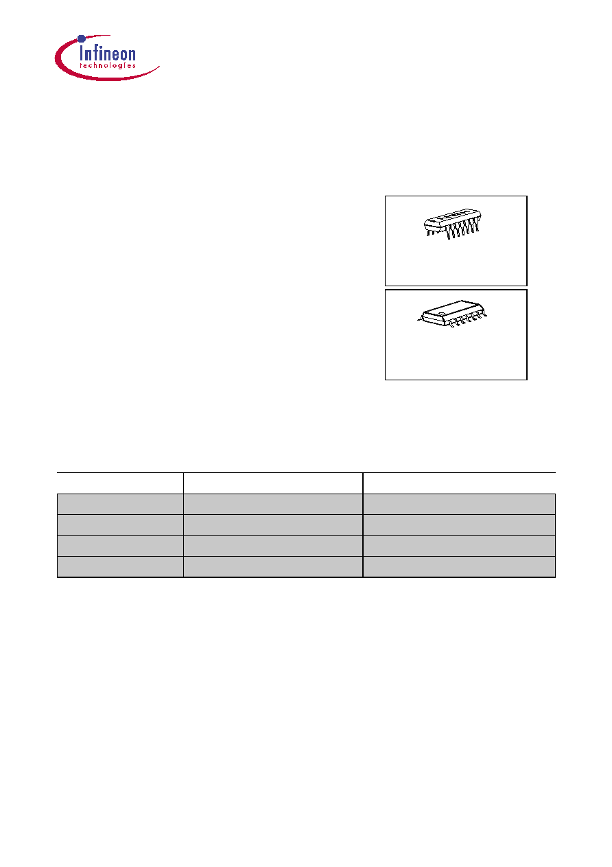
P-DSO-14-3
P-DIP-14-3
1
Overview
1.1
Features
· Line Current Consumption with PFC
· Low Power Consumption
· Stable and Adjustable Standby Frequency
· Very Low Start-up Current
· Soft-Start for Quiet Start-up
· Free usable Fault Comparators
· Synchronization and Fixed Frequency Facility
· Over- and Undervoltage Lockout
· Switch Off at Mains Undervoltage
· Temporary high power circuit (only TDA 16847)
· Mains Voltage Dependent Fold Back Point Correction
· Continuous Frequency Reduction with Decreasing Load
· Adjustable and Voltage Dependent Ringing Suppression Time
1.2
Description
The TDA 16846 is optimized to control free running or fixed frequency flyback converters
with or without Power Factor Correction (Current Pump). To provide low power
consumption at light loads, this device reduces the switching frequency continuously
with load, towards an adjustable minimum (e. g. 20 kHz in standby mode). Additionally,
the start up current is very low. To avoid switching stresses of the power devices, the
power transistor is always switched on at minimum voltage. A special circuit is
implemented to avoid jitter. The device has several protection functions:
V
CC
over- and
undervoltage, mains undervoltage, current limiting and 2 free usable fault comparators.
Regulation can be done by using the internal error amplifier or an opto coupler feedback
(additional input). The output driver is ideally suited for driving a power MOSFET, but it
can also be used for a bipolar transistor. Fixed frequency and synchronized operation
are also possible.
Type
Ordering Code
Package
TDA 16846
Q67000-A9377
P-DIP-14-3
TDA 16847
Q67000-A9378
P-DIP-14-3
TDA 16846G
Q67006-A9430
P-DSO-14-3
TDA 16847G
Q67006-A9412
P-DSO-14-3
TDA 16846
TDA 16847
Data Sheet
4
2000-01-14
The TDA 16846 is suited for TV-, VCR- sets and SAT receivers. It also can be good used
in PC monitors.
The TDA 16847 is identical with TDA 16846 but has an additional power measurement
output (pin 8) which can be used for a Temporary High Power Circuit.
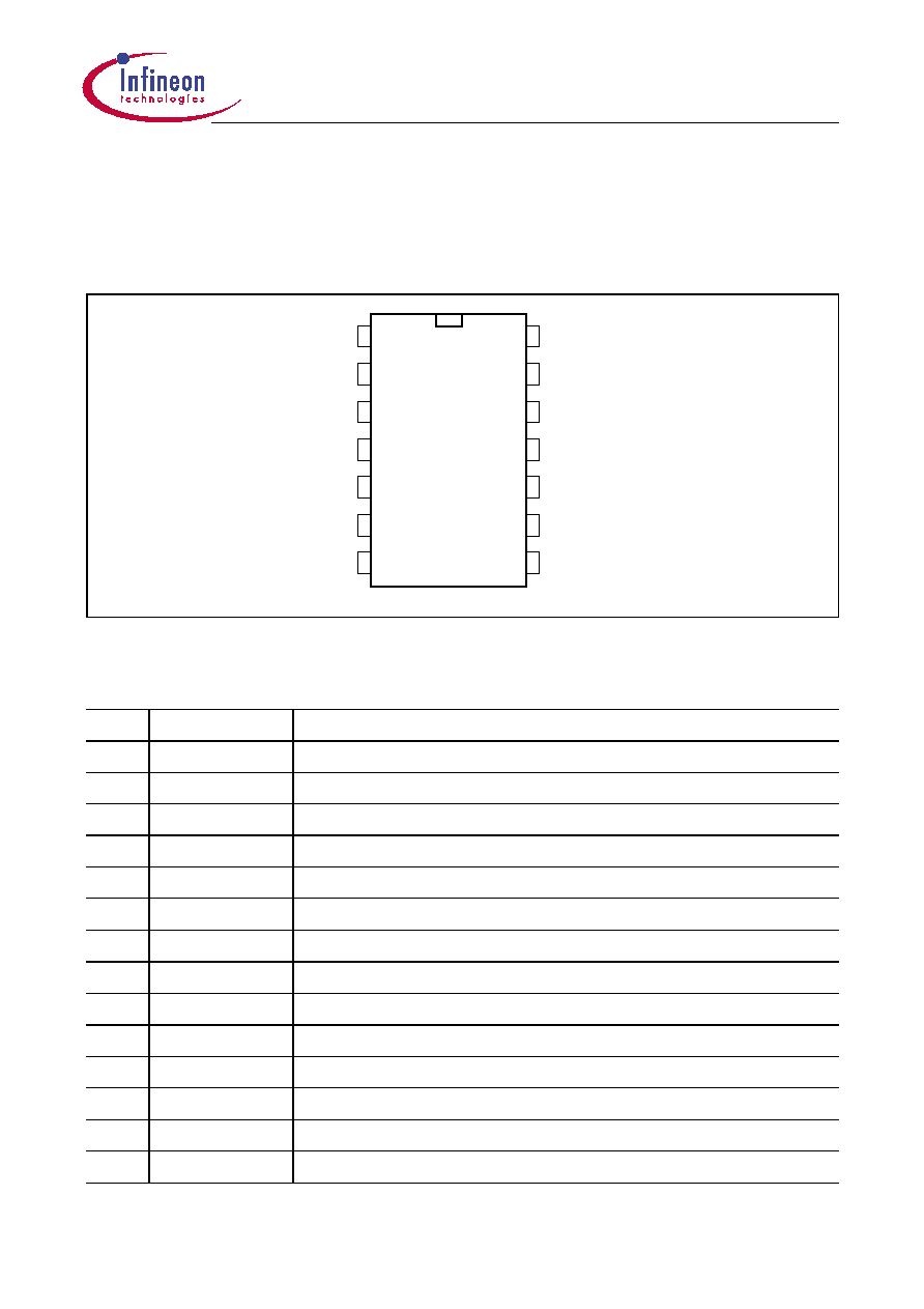
Figure 1
Pin Configuration (top view)
1.3
Pin Definitions and Functions
Pin
Symbol
Function
1
OTC
Off Time Circuit
2
PCS
Primary Current Simulation
3
RZI
Regulation and Zero Crossing Input
4
SRC
Soft-Start and Regulation Capacitor
5
OCI
Opto Coupler Input
6
FC2
Fault Comparator 2
7
SYN
Synchronization Input
8
N.C./PMO
Not Connected (TDA 16846)/PMO (TDA 16847)
9
REF
Reference Voltage and Current
10
FC1
Fault Comparator 1
11
PVC
Primary Voltage Check
12
GND
Ground
13
OUT
Output
14
VCC
Supply Voltage
10
8
9
1
2
3
4
5
6
14
7
13
12
OTC
11
PCS
RZI
SRC
OCI
FC2
SYN
N.C./PMO
REF
FC1
PVC
GND
OUT
AEP02647
VCC

TDA 16846
TDA 16847
Data Sheet
5
2000-01-14
1.4
Short Description of the Pin Functions
Pin
Function
1
A parallel RC-circuit between this pin and ground determines the ringing
suppression time and the standby-frequency.
2
A capacitor between this pin and ground and a resistor between this pin and
the positive terminal of the primary elcap quantifies the max. possible output
power of the SMPS.
3
This is the input of the error amplifier and the zero crossing input. The output
of a voltage divider between the control winding and ground is connected to
this input. If the pulses at pin 3 exceed a 5 V threshold, the control voltage at
pin 4 is lowered.
4
This is the pin for the control voltage. A capacitor has to be connected
between this pin and ground. The value of this capacitor determines the
duration of the softstart and the speed of the control.
5
If an opto coupler for the control is used, it's output has to be connected
between this pin and ground. The voltage divider at pin 3 has then to be
changed, so that the pulses at pin 3 are below 5 V.
6
Fault comparator 2: If a voltage > 1.2 V is applied to this pin, the SMPS stops.
7
If fixed frequency mode is wanted, a parallel RC circuit has to be connected
between this pin and ground. The RC-value determines the frequency. If
synchronized mode is wanted, sync pulses have to be fed into this pin.
8
Not connected (TDA 16846). / This is the power measurement output of the
Temporary High Power Circuit. A capacitor and a RC-circuit has to be
connected between this pin and ground (TDA 16847).
9
Output for reference voltage (5 V). With a resistor between this pin and ground
the fault comparator 2 (pin 6) is enabled.
10
Fault comparator 1: If a voltage > 1 V is applied to this pin, the SMPS stops.
11
This is the input of the primary voltage check. The voltage at the anode of the
primary elcap has to be fed to this pin via a voltage divider. If the voltage of
this pin falls below 1 V, the SMPS is switched off. A second function of this pin
is the primary voltage dependent fold back point correction (only active in free
running mode).
12
Common ground.
13
Output signal. This pin has to be connected across a serial resistor with the
gate of the power transistor.
14
Connection for supply voltage and startup capacitor. After startup the supply
voltage is produced by the control winding of the transformer and rectified by
an external diode.
TDA 16846
TDA 16847
Data Sheet
6
2000-01-14
1.5
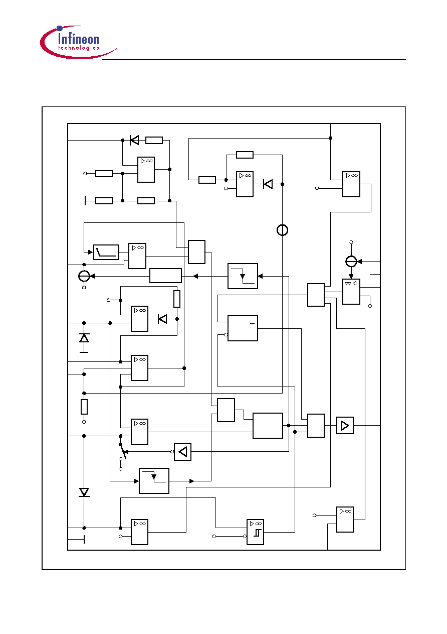
Block Diagrams
Figure 2
TDA 16846
AEB02648
-
+
+
-
4
R
D4
R
7
5 V
30 k
R
8
75 k
R
3
15 k
Control Voltage
KSY
+
-
PVA
1.5 V
6
R
6
R
D5
Fold Back Point Correction
1 V
+
-
Voltage
Check
-
+
CC
V
1.2 V
1
&
Off Time
Comparator
2 V
Limit
G1
3.5 V
-
+
D2
Error
Amplifier
R
2
5 V
D3
Control Voltage
-
+
Buffer for
5 V
-
+
Comparator
Overvoltage
1
R
20 k
< 25 mV
1.5 V
I
ED1
16 V
Comparator
-
+
On Time
D1
Startup
G4
1
Q
S
R
ED2
Error-
Flipflop
On Time
Flipflop
R
S
Q
G2
Voltage
Comparator
-
+
15/8 V
Zero Crossing
Signal
&
Output
Driver
Primary
+
-
FC1
1 V
7
1
SYN
OTC
RZI
3
4
SRC
5
OCI
PCS
2
14
GND
12
CC
V
10
FC1
13
OUT
6
FC2
REF
9
N.C.
8
11
PVC
x 1/3
1
Diode
Supply
The input with the lower voltage becomes operative
1)
FC2
+
G3
CS1
RSTC/RSTF
3.5 V
-
+
TDA 16846
TDA 16847
Data Sheet
7
2000-01-14
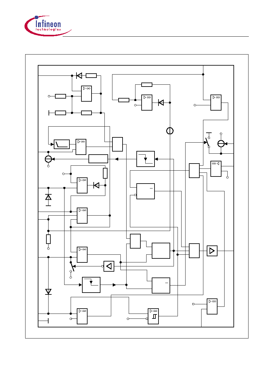
Figure 3
TDA 16847
AEB02737
-
+
+
-
4
R
D4
R
7
5 V
30 k
R
8
75 k
R
3
15 k
Control Voltage
KSY
+
-
PVA
1.5 V
6
R
6
R
D5
Fold Back Point Correction
1 V
+
-
Voltage
Check
-
+
CC
V
1.2 V
1
&
Off Time
Comparator
2 V
Limit
G1
3.5 V
-
+
D2
Error
Amplifier
R
2
5 V
D3
Control Voltage
-
+
Buffer for
5 V
-
+
Comparator
Overvoltage
1
R
20 k
< 25 mV
1.5 V
I
ED1
16 V
Comparator
-
+
On Time
D1
Startup
G4
1
Q
S
R
ED2
Error-
Flipflop
On Time
Flipflop
R
S
Q
G2
Supply Voltage
Comparator
-
+
15/8 V
Crossing
Signal
&
Output
Driver
Primary
+
-
FC1
1 V
7
1
SYN
OTC
RZI
3
4
SRC
5
OCI
PCS
2
14
GND
12
CC
V
10
FC1
13
OUT
6
FC2
REF
9
PMO
8
11
PVC
x 1/3
1
Diode
The input with the lower voltage becomes operative
1)
FC2
+
G3
CS1
RSTC/RSTF
3.5 V
-
+
S1
S2
Zero
Q
R
Flipflop
Discharge Time
S
1)
TDA 16846
TDA 16847
Data Sheet
8
2000-01-14
2
Functional Description
Start Up Behaviour (Pin 14)
When power is applied to the chip and the voltage
V
14
at Pin 14 (
V
CC
) is less than the
upper threshold (
V
ON
) of the Supply Voltage Comparator (SVC), input current
I
14
will be
less than 100
µ
A. The chip is not active and driver output (Pin 13) and control output
(Pin 4) will be actively held low. When
V
14
exceeds the upper SVC threshold (
V
ON
) the
chip starts working and
I
14
increases. When
V
14
falls below the lower SVC threshold
(
V
OFF
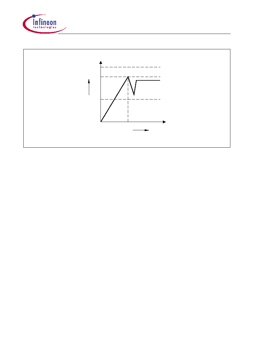
) the chip starts again at his initial condition. Figure 4 shows the start-up circuit and
Figure 5 shows the voltage
V
14
during start up. Charging of
C
14
is done by resistor
R
2
of
the "Primary Current Simulation" (see later) and the internal diode D1, so no additional
start up resistor is needed. The capacitor
C
14
delivers the supply current until the
auxiliary winding of the transformer supplies the chip with current through the external
diode D14.
It is recommended to switch a small RF snubber capacitor of e.g. 100 nF parallel to the
electrolytic capacitor at pin 14 as shown in the application circuits in Figures 15, 16, and
17.
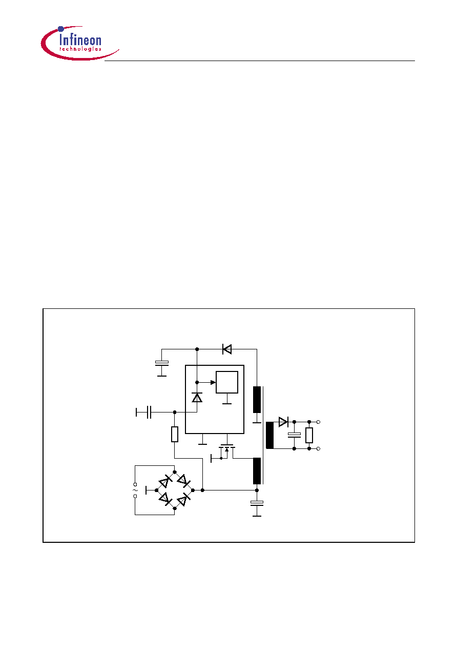
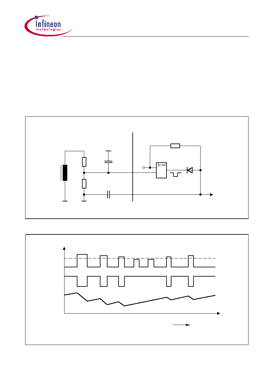
Figure 4
Startup Circuit
AES02649
SVC
TDA 16846
D1
2
14
CC
V
PCS
2
C
R
2
C
14
C
p
Out
V
TR
D14
TDA 16846
TDA 16847
Data Sheet
9
2000-01-14
Figure 5
Startup Voltage Diagram
Primary Current Simulation PCS (Pin 2) / Current Limiting
A voltage proportional to the current of the power transistor is generated at Pin 2 by the
RC-combination
R
2
,
C
2
(Figure 4). The voltage at Pin 2 is forced to 1.5 V when the
power transistor is switched off and during its switch on time
C
2
is charged by
R
2
from
the rectified mains. The relation of
V
2
and the current in the power transistor (
I
primary
) is
:
L
primary
: Primary inductance of the transformer
The voltage
V
2
is applied to one input of the On Time Comparator ONTC (see Figure 2).
The other input is the control voltage. If
V
2
exceeds the control voltage, the driver
switches off (current limiting). The maximum value of the control voltage is the internal
reference voltage 5 V, so the maximum current in the power transistor (
I
Mprimary
) is
:
The control voltage can be reduced by either the Error Amplifier EA (current mode
regulation), or by an opto coupler at Pin 5 (regulation with opto coupler isolation) or by
the voltage
V
11
at Pin 11 (Fold Back Point Correction).
AED02650
t
Startup
Operation
14
V
V
max
On
V
V
Off
V
2
1,5 V
L
pr imary
I
primary
×
R
2
C
2
×
--------------------------------
+
=
I
Mprimar y
3,5 V
R
2
×
C
2
×
L
primary
--------------------------------------
=

TDA 16846
TDA 16847
Data Sheet
10
2000-01-14
Fold Back Point Correction PVC (Pin 11)
V
11
is deviated by a voltage divider from the rectified mains and reduces the limit of the
possible current maximum in the power transistor if the mains voltage increases. I.e. this
limit is independent of the mains (only active in free running mode). The maximum
current (
I
Mprimary
) depending on the voltage
V
11
at Pin 11 is
:
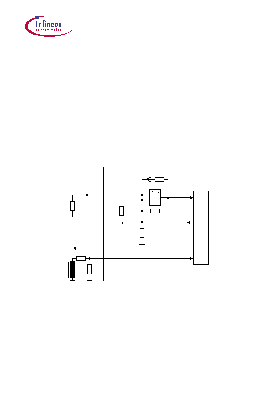
Off-Time Circuit OTC (Pin 1)
Figure 6 shows the Off-Time Circuit which determines the load dependent frequency
course. When the driver switches off (Figure 7) the capacitor
C
1
is charged by current
I
1
(approx. 1 mA) until the capacitor's voltage reaches 3.5 V. The charge time TC1 is
:
For proper operation of the special internal anti jitter circuit, TC1 should have the same
value as the resonance time "TR" of the power circuit (Figure 7). After charging
C
1
up to
3.5 V the current source is disconnected and
C
1
is discharged by resistor
R
1
. The voltage
V
1
at Pin 1 is applied to the Off-Time Comparator (OFTC). The other input of OFTC is
the control voltage. The value of the control voltage at the input of OFTC is limited to a
minimum of 2 V (for stable frequency at very light load). The On-Time Flip Flop (ONTF)
is set, if the output of OFTC is high
1)
and the voltage
V
3
at Pin 3 falls below 25 mV (zero
crossing signal is high). This ensures switching on of the power transistor at minimum
voltage. If no zero crossing signal is coming into pin 3, the power transistor is switched
on after an additional delay until
V
1
falls below 1.5 V (see Figure 6, OFTCD). As long as
V
1
is higher than the limited control voltage, ONTF is disabled to suppress wrong zero
crossings of
V
3
, due to parasitic oscillations from the transformer after switch-off. The
discharge time of
C
1
is a function of the control voltage.
1)
i.e.
V
1
is less than the limited control voltage.
.
If the control voltage is below 2 V (at low output power) the "off-time" is maximum and
constant
Control Voltage
Output Power
Off-time TD1
1.5 - 2 V
Low
Constant (TD1
MAX.
), const. frequency stand by
2 - 3.5 V
Medium
Decreasing
3.5 - 5 V
High
Free running, switch-on at first minimum
I
Mprimar y
4 V
V
11
3
/
(
)
R
2
C
2
×
×
L
primary
------------------------------------------------------------
=
TC1
C
1
1,5 V
×
1mA
-------------------------
TD1
max
0,47
R
1
×
C
1
×
TDA 16846
TDA 16847
Data Sheet
11
2000-01-14
Figure 6
Off-Time-Circuit
AES02651
1
-
+
OFTC
&
ED3
Limit
2 V
Control Voltage
ED2
2 V
S
Q
R
ONTF
&
Output
Driver
From SYNC
From ONTC
From UVLO
RSTC
S
R
Q
Ringing Suppression Time
ED1
-
+
RSTC
Zero Crossing Signal
1
I
3.5 V
Internal
External
1
R
C
1
1
OTC
From Error FF
RZI 3
OFTCD
+
-
1.5 V
1
TDA 16846
TDA 16847
Data Sheet
12
2000-01-14
Figure 7
Pulse Diagram of Off-Time-Circuit
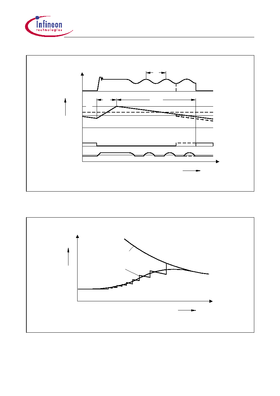
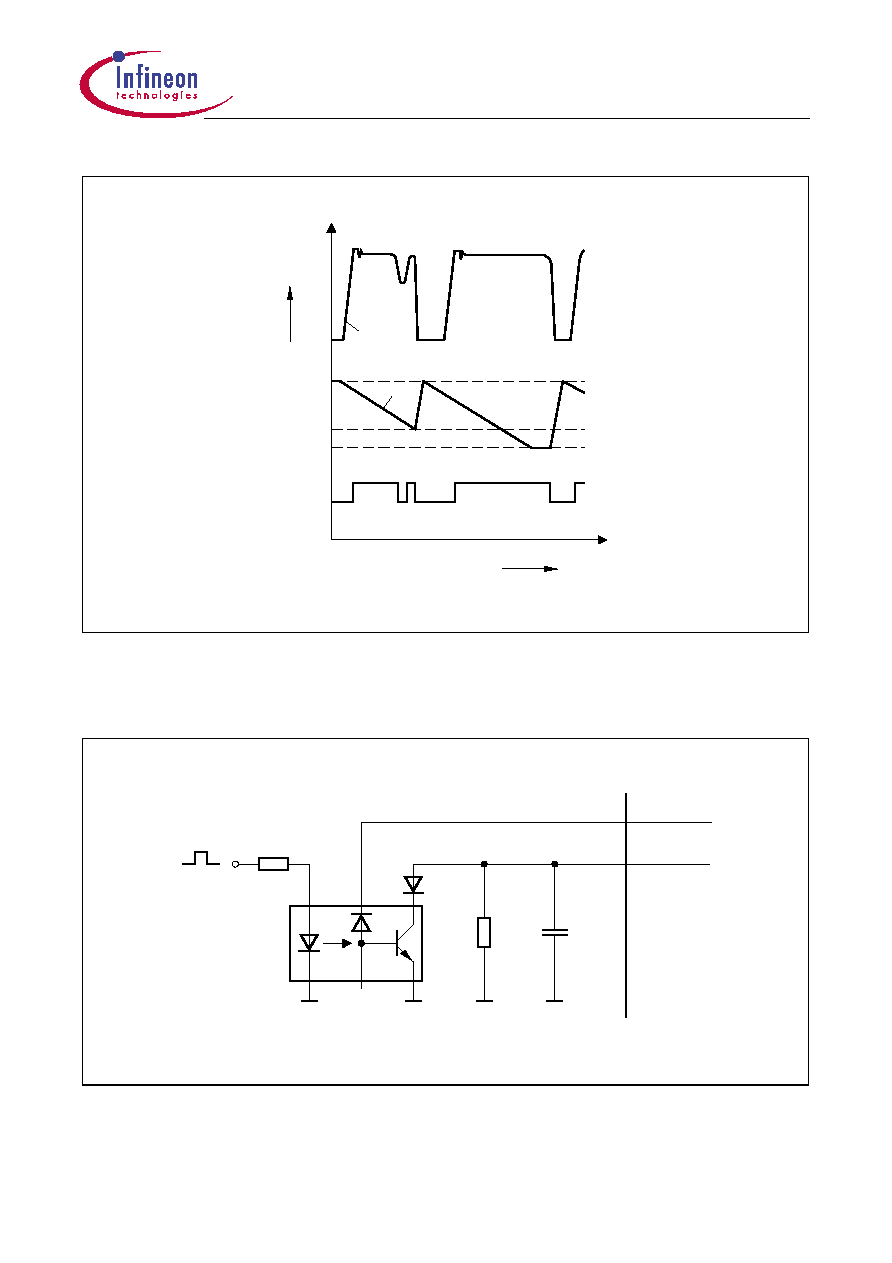
Figure 8 shows the converters switching frequency as a function of the output power.
Figure 8
Load Dependant Frequency Course
AED02652
t
0 V
2 V
3.5 V
3
V
V
13
V
Drain
Trans.
Power
V
5
1
V
C1
t
t
D1max
t
R
AED02653
f
OUT
Conventional
Free Running
TDA 16846
e.g. 20 kHz
P
TDA 16846
TDA 16847
Data Sheet
13
2000-01-14
Error Amplifier EA / Soft-Start (Pin 3, Pin 4)
Figure 9 shows the simplified Error Amplifier circuit. The positive input of the Error
Amplifier (EA) is the reference voltage 5 V. The negative input is the pulsed output
voltage from the auxiliary winding, divided by
R
31
and
R
32
. The capacitor
C
3
is
dimensioned only for delaying zero crossings and smoothing the first spike after switch-
off. Smoothing of the regulation voltage is done with the soft start capacitor
C
4
at Pin 4.
During start up
C
4
is charged with a current of approx. 2
µ
A (Soft Start). Figure 10 shows
the voltage diagrams of the Error Amplifier circuit.
Figure 9
Error Amplifier
Figure 10
Regulation Pulse Diagram
AES02654
-
+
Amplifier
5 V
Down
3
4
Reg
V
TR
4
C
3
C
Internal
External
31
R
32
R
RZI
SRC
Error
AED02655
t
Ref
V
3
V
V
4
Down
TDA 16846
TDA 16847
Data Sheet
14
2000-01-14
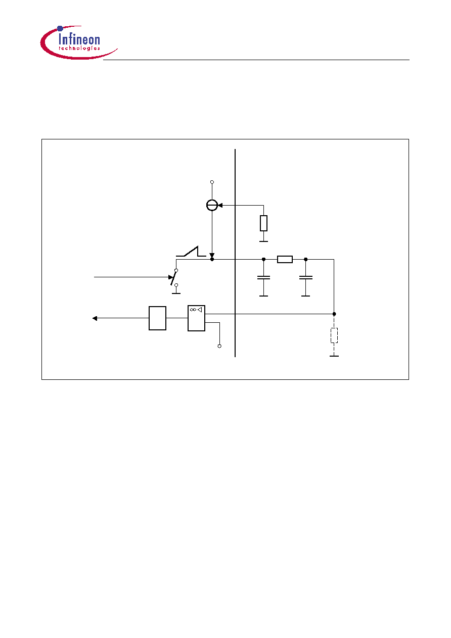
Fixed Frequency and Synchronization Circuit SYN (Pin 7)
Figure 11 shows the Fixed Frequency and Synchronization Circuit. The circuit is
disabled when Pin 7 is not connected. With
R
7
and
C
7
at Pin 7 the circuit is working.
C
7
is charged fast by approx. 1 mA and discharged slowly by
R
7
(Figure 11). The power
transistor is switched on at beginning of the charge phase. The switching frequency is
(charge time ignored)
:
When the oscillator circuit is working the Fold Back Point Correction is disabled (not
necessary in fixed frequency mode). "Switch on" is only possible when a "zero crossing"
has occurred at Pin 3, otherwise "switch-on" will be delayed (Figure 12).
Figure 11
Synchronization and Fixed Frequency Circuit
f
1,18
R
7
C
7
×
--------------
AES02656
-
+
15 k
75 k
5 V
7
R
C
7
SYN 7
Logic
OUT
RZI
13
3
Zero Crossing Signal
External
Internal
30
OP1OUT
OP1
k
LO
TDA 16846
TDA 16847
Data Sheet
15
2000-01-14
Figure 12
Pulse Diagram for Fixed Frequency Circuit
Synchronization mode is also possible. The synchronization frequency must be higher
than the oscillator frequency.
Figure 13
Ext. Synchronization Circuit
AED02657
t
0.7 V
RZI(3)
1.5 V
3.6 V
V
Trans
V
7
V
AES02658
5 V 470
SFH 6136
7
R
39 k
7
C
1 nF
9
7
Internal
External
SYN

TDA 16846
TDA 16847
Data Sheet
16
2000-01-14
3
Protection Functions
The chip has several protection functions:
Current Limiting
See "Primary Current Simulation PCS (Pin 2) / Current Limiting" and "Fold Back Point
Correction PVC (Pin 11)".
Over- and Undervoltage Lockout OV/SVC (Pin 14)
When
V
14
at Pin 14 exceeds 16 V, e. g. due to a fault in the regulation circuit, the Error
Flip Flop ERR is set and the output driver is shut-down. When
V
14
goes below the lower
SVC threshold, ERR is reset and the driver output (Pin 13) and the soft-start (Pin 4) are
shut down and actively held low.
Primary Voltage Check PVC (Pin 11)
When the voltage
V
11
at Pin 11 goes below 1 V the Error Flip Flop (ERR) is set. E.g. a
voltage divider from the rectified mains at Pin 11 prevents from high input currents at too
low input voltage.
Free Usable Fault Comparator FC1 (Pin 10)
When the voltage at Pin 10 exceeds 1 V, the Error Flip Flop (ERR) is set. This can be
used e. g. for mains overvoltage shutdown.
Free Usable Fault Comparator FC2 (Pin 6)
When the voltage at Pin 6 exceeds 1.2 V, the Error Flip Flop (ERR) is set. A resistor
between Pin 9 (REF) and ground is necessary to enable this fault comparator.
Voltage dependent Ringing Suppression Time
During start-up and short-circuit operation, the output voltage of the converter is low and
parasitic zero crossings are applied for a longer time at Pin 3. Therefore the Ringing
Suppression Time TC1 (see "Off-Time Circuit OTC (Pin 1)") is made longer with
factor 2.5 at low output voltage. To ensure start-up of the circuit, the value of resistor
R
1
(Pin 1, Figure 6) must be higher than 20 k
.
TDA 16846
TDA 16847
Data Sheet
17
2000-01-14
4
Temporary High Power Circuit FC2, PMO, REF
(Pin 6, 8, 9, TDA 16847)
Figure 14 shows the Temporary High Power Circuit:
Figure 14
The Temporary High Power Circuit (THPC) consists of two parts:
First a power measurement circuit is implemented: The capacitor
C
8
at Pin 8 is charged
with a constant current
I
8
during the discharge time of the flyback transformer and
connected to ground the other time. So the average of the sawtooth voltage
V
8
at Pin 8
is proportional to the converters output power (at constant output voltages). The charge
current
I
8
for
C
8
is dimensioned by the resistor
R
9
at Pin 9:
I
8
= 5 V/
R
9
-
+
1.2 V
1
6 FC2
REF
9
8
FC2
S2
to Error Flipflop
Discharge Time
CS2
CC
V
51 k
R
9
8
C
C
6
8
R
PMO
6
10 M
R
Internal
External
AEB02739
I
8

TDA 16846
TDA 16847
Data Sheet
18
2000-01-14
Second a High Power Shutdown Comparator (FC2) is implemented: When the voltage
V
6
at Pin 6 exceeds 1.2 V the Error Flip Flop (ERR) is set. The output voltage of the
power measurement circuit (Pin 8) is smoothed by
R
8
/
C
6
and applied to the "high power
shutdown" input at Pin 6. The relation between this voltage
V
6
and the output power of
the converter
P
is approximately:
V
6
(
P
×
L
Secondary
×
5 V)/(
V
OUT
2
×
C
8
×
R
9
)
L
Secondary
: The transformers secondary inductance
V
OUT
: The converters output voltage
So the time constant of
R
9
/
C
8
for a certain high power shutdown level
P
SD
is:
R
9
×
C
8
(
P
SD
×
L
Secondary
×
4.2)/
V
OUT
2
The converters high power shutdown level can be dimensioned lower (by
R
9
,
C
8
) than
the current limit level (see "current limiting"). So because of the delay
R
8
/
C
6
, the
converter can deliver maximum output power (current limit level) for a certain time (e. g.
for power pulses like motor start current) and a power below the high power shutdown
level for unlimited time. This has the advantage that the thermal dimensioning of the
power devices is only needed for the lower power level. Once the voltage
V
6
exceeds
1.2 V there are no more charge or discharge actions at Pin 8. The voltage
V
6
remains
high due to the bias current out of HPC and the converter remains switched-off. Reset
can be done by either plug-off the supply from the mains or with a high value resistor
R
6
(Figure 14).
R
6
causes a reset every view seconds. When Pin 9 is not connected or gets
too less current the temporary high power circuit is disabled.

TDA 16846
TDA 16847
Data Sheet
19
2000-01-14
5
Electrical Characteristics
Note: Stresses above those listed here may cause permanent damage to the device.
Exposure to absolute maximum rating conditions for extended periods may affect
device reliability.
5.1
Absolute Maximum Ratings
All voltages listed are referenced to ground (0 V,
V
SS
) except where noted.
Parameter
Symbol
Limit Values
Unit Remarks
min.
max.
Supply Voltage at Pin 14
V
CC
0.3
17
V
Voltage at Pin 1, 4, 5, 6, 7, 9, 10
0.3
6
V
Voltage at Pin 2, 8, 11
0.3
17
V
Voltage at Pin 3
Current into Pin 3
RZI
10
6
V
mA
V
3
< 0.3 V
Current into Pin 9
REF
1
mA
Current into Pin 13
OUT
100
100
mA
mA
V
13
>
V
CC
V
13
< 0 V
ESD Protection
2
kV
MIL STD 883C
method 3015.6,
100 pF, 1500
Storage Temperature
T
stg
65
125
°
C
Operating Junction Temperature
T
J
25
125
°
C
Thermal Resistance
Junction-Ambient
R
thJA
110
K/W P-DIP-14-3
Soldering Temperature
260
°
C
Soldering Time
10
s

TDA 16846
TDA 16847
Data Sheet
20
2000-01-14
5.2
Characteristics
Unless otherwise stated, 25
°
C <
T
j
< 125
°
C,
V
CC
= 12 V
Parameter
Symbol
Limit Values
Unit Test Condition
min.
typ.
max.
Start-Up Circuit
Supply current, OFF
I
14
40
100
µ
A
0 <
V
CC
<
V
14
ON
Supply current, ON
I
14
5
8
mA
Output low
Turn-ON threshold
V
14
ON
14.5
15
15.5
V
Turn-OFF threshold
V
14
OFF
7.5
8
8.5
V
Primary Current Simulation PCS (Pin 2) / Current Limiting
Basic value
V
2
1.45
1.5
1.55
V
I
2
= 100
µ
A
Peak value
V
2
4.85
5
5.15
V
V
11
= 1.2 V
On-time
9.0
10.5
11.5
µ
s
V
11
= 1.2 V,
C
2
= 220 pF,
I
2
= 75
µ
A
Bias current Pin 2
1.0
0.3
µ
A
Fold Back Point Correction PVC (Pin 11)
Peak value
V
2
3.8
4.1
4.3
V
V
11
= 4.5 V
On-time
6.2
7.5
8.5
µ
s
V
11
= 4.5 V,
C
2
= 220 pF,
I
2
= 75
µ
A
Bias current Pin 11
1.0
0.3
µ
A
Off-Time Circuit OTC (Pin 1)
Charge current
I
1
0.9
1.1
1.4
mA
V
3
> 3 V
Charge current
I
1
0.35
0.5
0.65
mA
V
3
< 2 V
Peak value
V
1
3.38
3.5
3.62
V
Basic value
V
1
1.92
2
2.08
V

TDA 16846
TDA 16847
Data Sheet
21
2000-01-14
T12 Charge time
TC1
0.85
1.0
1.3
µ
s
V
3
> 3 V,
C
1
= 680 pF,
R
1
= 100 k
T13 Charge time
TC1
1.9
2.4
3.0
µ
s
V
3
< 2 V,
C
1
= 680 pF,
R
1
= 100 k
Off-time
TD1
MAX.
65
72
80
µ
s
C
1
= 680 pF,
R
1
= 100 k
Bias current Pin 1
1.1
0.4
µ
A
Zero crossing threshold
(Pin 3)
15
25
35
mV
Delay to switch-on
280
350
480
ns
Bias current Pin 3
2
1.2
µ
A
V
3
< 25 mV
Error Amplifier EA (Pin 3, Pin 4)
Input threshold (Pin 3)
V
EATH
4.85
5
5.15
V
Bias current Pin 3
0.9
µ
A
V
3
> 3 V
Soft-start charge current
(Pin 4)
2.5
1.8
1.2
µ
A
Opto Coupler Input (Pin 5)
Input voltage range
V
5
0.3
6
V
Pull high resistor to
V
REF
R
1
15
20
25
k
5.2
Characteristics (cont'd)
Unless otherwise stated, 25
°
C <
T
j
< 125
°
C,
V
CC
= 12 V
Parameter
Symbol
Limit Values
Unit Test Condition
min.
typ.
max.

TDA 16846
TDA 16847
Data Sheet
22
2000-01-14
Fixed Frequency and Synchronization Circuit SYN (Pin 7)
Frequency
78
88
98
kHz
C
7
= 470 pF,
R
7
= 20 k
Charge current
I
7
1.0
1.3
1.6
mA
Upper threshold
V
7
3.5
3.6
3.7
V
Lower threshold
V
7
1.43
1.5
1.57
V
Charge time
0.4
0.55
0.75
µ
s
Bias current Pin 7
2.4
1.8
1.1
µ
A
Input voltage range
V
7
0.3
6
V
Undervoltage Lockout SVC (Pin 14)
Threshold
V
14
OFF
7.5
8
8.5
V
Overvoltage Lockout OV (Pin 14)
Threshold
V
14 OV
15.7
16.5
17
V
Delta-OV-
V
14 ON
0.5
V
Primary Voltage Check PVC (Pin 11)
Threshold
V
11
0.95
1
1.06
V
Reference Voltage (Pin 9)
Voltage at Pin 9
V
9
4.8
5
5.15
V
I
9
= 100
µ
A
Current into Pin 9
I
9
200
0
µ
A
V
EATH(Pin 3)
V
9
< 50 mV
5.2
Characteristics (cont'd)
Unless otherwise stated, 25
°
C <
T
j
< 125
°
C,
V
CC
= 12 V
Parameter
Symbol
Limit Values
Unit Test Condition
min.
typ.
max.

TDA 16846
TDA 16847
Data Sheet
23
2000-01-14
Note: The listed characteristics are ensured over the operating range of the integrated
circuit. Typical characteristics specify mean values expected over the production
spread. If not otherwise specified, typical characteristics apply at
T
A
= 25
°
C and
the given supply voltage.
Fault Comparator FC2 (Pin 6)
HPC Threshold
V
6
1.12
1.2
1.28
V
Bias Current Pin 6
1.0
0.3
0.1
µ
A
Fault Comparator FC1 (Pin 10)
Threshold
V
10
0.95
1
1.06
V
Bias current Pin 10
0.48
0.9
1.2
µ
A
Power Measurement Output PMO (Pin 8, only TDA 16847)
Charge current Pin 8
I
8
110 100 90
µ
A
I
9
= 100
µ
A
Output Driver OD (Pin 13)
Output voltage low state
V
13
low
1.1
1.8
2.4
V
I
13
= 100 mA
Output voltage high state
V
13
high
9.2
10
11
V
I
13
= 100 mA
Output voltage during low
supply voltage
V
13
aclow
0.8
1.8
2.5
V
I
13
= 10 mA,
V
14
increasing:
0 <
V
14
<
V
14
ON
V
14
decreasing:
0 <
V
14
<
V
14
OFF
Rise time
70
110
180
ns
C
13
= 10 nF,
V
13
= 2 ... 8 V
Fall time
30
50
80
ns
C
13
= 10 nF,
V
13
= 2 ... 8 V
5.2
Characteristics (cont'd)
Unless otherwise stated, 25
°
C <
T
j
< 125
°
C,
V
CC
= 12 V
Parameter
Symbol
Limit Values
Unit Test Condition
min.
typ.
max.
TDA 16846
TDA 16847
Data Sheet
24
2000-01-14
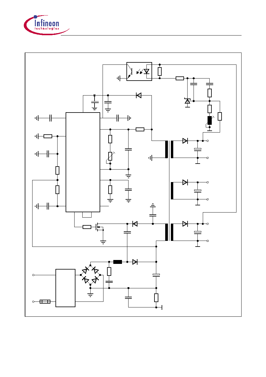
Figure 15
Circuit Diagram for Application with PFC
AES02659
25
C
10 nF
4
R
24
18 k
11
1 nF
24
C
23
R
3.9 M
1 M
R
22
560 pF
22
C
2
5
3
29
R
9.1 k
2 k
P
10
6, 10, 12
C
22
150 pF
56 k
R
30
1.5 nF
30
C
8
N.C.
9.1 k
38
R
µ
220 F
C
41
TR1
(AL = 190 nH)
D41
MUR4100
52 Turns
7 Turns
1
V
100 V
MUR120
9 Turns
D42
F
470
µ
V
16 V
42
C
2
MUR120
5 Turns
D43
8.5 V
µ
V
470
43
C
3
F
µ
22
26
C
F
1N4148
D26
13
7
9
R
35
15
MUR4100
D9
C
9
220 pF
8
L
2 mH
C
10 nF
8
STTA506D
D8
µ
7
150
C
F/450 V
4.7 M
10
R
R
5
5.1 k
1 nF
C
5
D1-D4
4 x BYW 76
1 nF
C
10
RFI Filter
180-270 V
3.15 A
F1
TDA 16846
IC1
14
1
T1
54 Turns
C
28
4.7 nF
3
4
2
1
62
R
820
61
R
1 k
61
10 nF
C
1 nF
62
C
63
R
100 k
2.2 k
60
R
P
500
60
65
100 k
R
IC 02
SFH 617 A-2
SPP ( 0.6
)
N6055
C27
100 nF
TDA 16846
TDA 16847
Data Sheet
25
2000-01-14
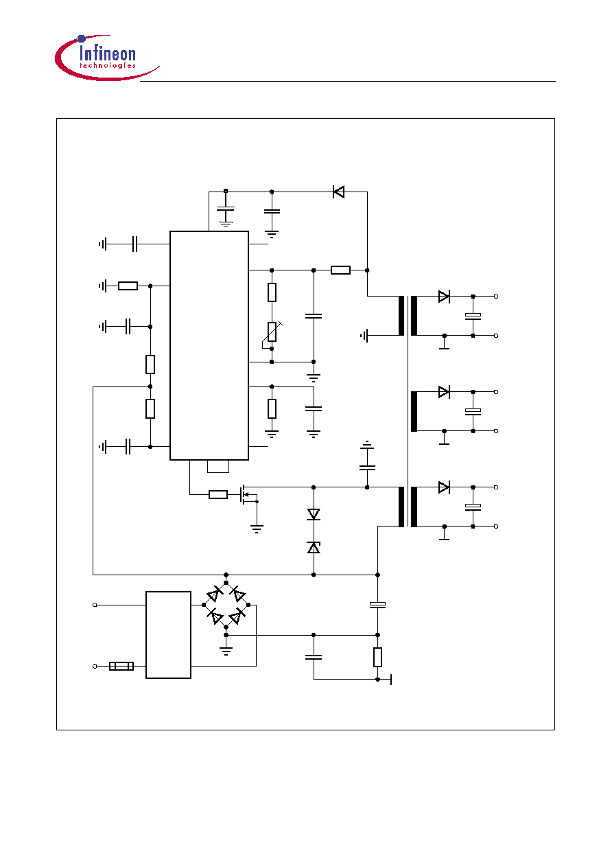
Figure 16
Circuit Diagram for Standard Application
AES02660
25
C
10 nF
4
R
24
18 k
11
1 nF
24
C
23
R
3.9 M
1 M
R
22
680 pF
22
C
2
5
3
29
R
9.1 k
2 k
P
10
6, 10, 12
C
22
150 pF
56 k
R
30
1.5 nF
30
C
8
N.C.
9.1 k
38
R
µ
220 F
C
41
TR1
(AL = 190 nH)
D41
MUR4100
52 Turns
7 Turns
1
V
100 V
MUR120
9 Turns
D42
F
470
µ
V
16 V
42
C
2
MUR120
5 Turns
D43
8.5 V
µ
V
470
43
C
3
F
µ
22
26
C
F
1N4148
D26
13
7
9
R
35
15
C
9
220 pF
µ
7
150
C
F/385 V
4.7 M
10
R
D1-D4
4 x 1N4007
1 nF
C
10
RFI Filter
180-270 V
3.15 A
F1
TDA 16846
IC1
14
1
77 Turns
D10
BA1 59
D11
T1
N6055
SPP (
1.4
)
C27
100 nF
TDA 16846
TDA 16847
Data Sheet
26
2000-01-14
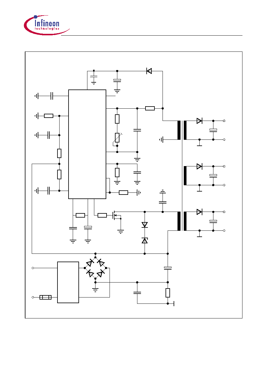
Figure 17
Circuit Diagram for Application with Temporary High Power Circuit
AES02738
25
C
10 nF
4
R
24
18 k
11
1 nF
24
C
23
R
3.9 M
1 M
R
22
680 pF
22
C
2
5
3
29
R
9.1 k
2 k
P
10
10, 12
C
22
150 pF
56 k
R
30
1.5 nF
30
C
9
9.1 k
38
R
µ
220 F
C
41
TR1
(AL = 190 nH)
D41
MUR4100
52 Turns
7 Turns
1
V
100 V
MUR120
9 Turns
D42
F
470
µ
V
16 V
42
C
2
MUR120
5 Turns
D43
8.5 V
µ
V
470
43
C
3
F
µ
22
26
C
F
1N4148
13
R
35
15
C
9
220 pF
µ
7
150
C
F/385 V
4.7 M
10
R
D1-D4
4 x 1N4007
1 nF
C
10
RFI Filter
180-270 V
3.15 A
F1
TDA 16847
IC1
14
1
77 Turns
D10
BA 159
D11
T1
N6055
SPP (
1.4
)
D26
7
32
R
51 k
33
R
1 M
C
31
100 pF
C
32
4.7
µ
F
6
8
C27
100 nF
TDA 16846
TDA 16847
Data Sheet
27
2000-01-14
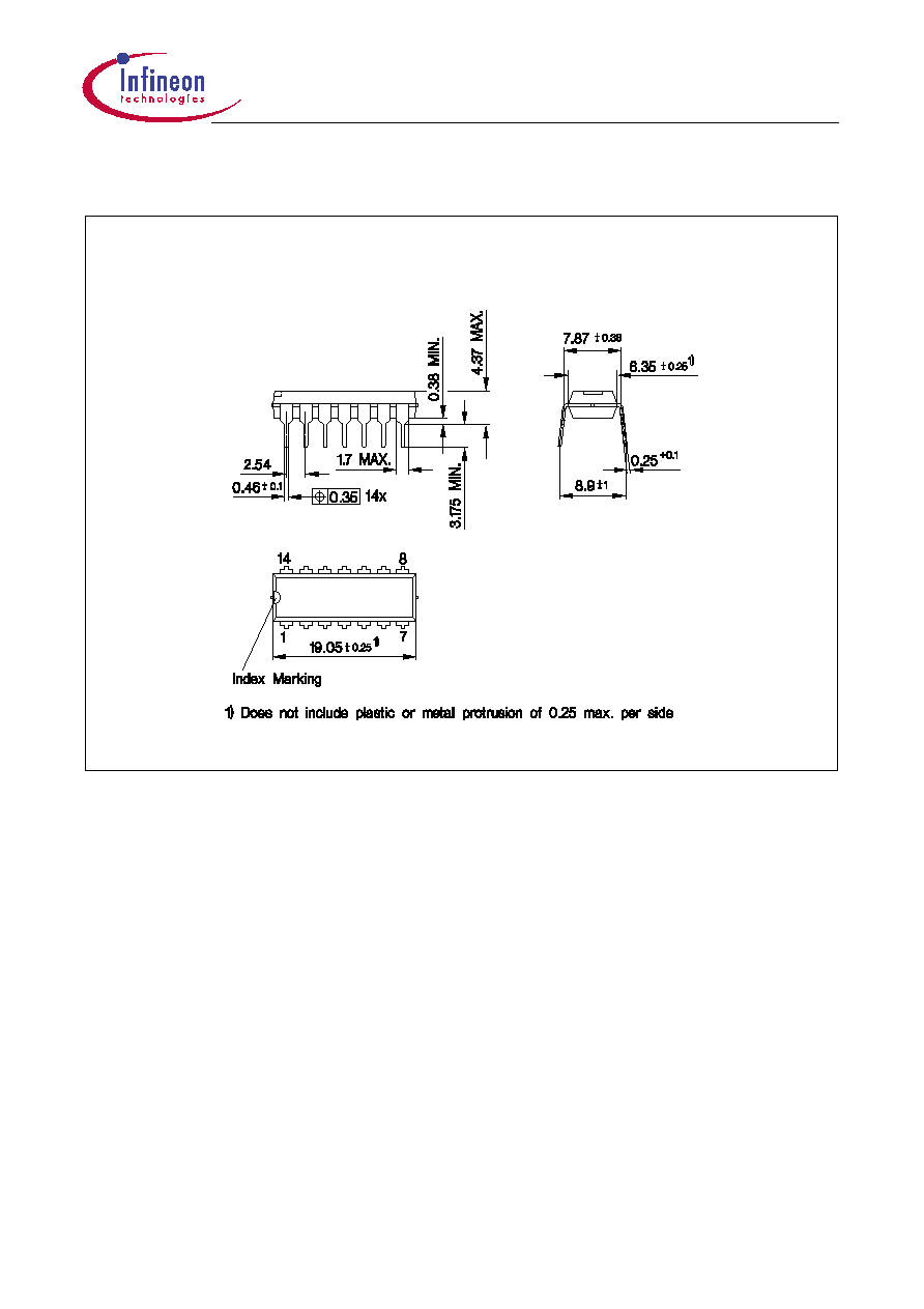
Package Outlines
P-DIP-14-3
(Plastic Dual In-line Package)
GP
D
0
558
4
Sorts of Packing
Package outlines for tubes, trays etc. are contained in our
Data Book "Package Information".
Dimensions in mm
TDA 16846
TDA 16847
Data Sheet
28
2000-01-14
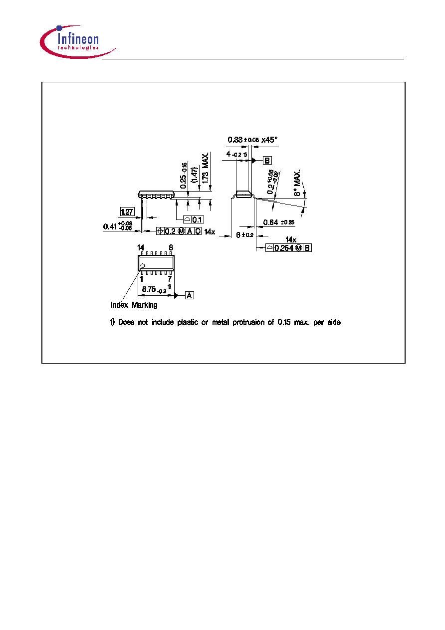
P-DSO-14-3
(Plastic Dual In-line Package)
Sorts of Packing
Package outlines for tubes, trays etc. are contained in our
Data Book "Package Information".
Dimensions in mm