
Fiber Optics
MARCH 2000
V23806-A34-C2
Single Mode FDDI 1x9 Transceiver with SC Receptacle
FEATURES
∑ Compliant with existing FDDI standard
∑ Compact integrated transceiver unit with
≠ MQW laser diode transmitter
≠ InGaAs PIN photodiode receiver
≠ Duplex SC receptacle
∑ Class 1 FDA and IEC laser safety compliant
∑ FDA Accession No. 9520890-21
∑ Single power supply (5 V)
∑ Signal detect indicator
∑ PECL differential inputs and outputs
∑ Process plug included
∑ Wave solderable and washable with process
plug inserted
∑ Industry standard multisource 1x9 footprint
Absolute Maximum Ratings
Exceeding any one of these values may destroy the device
immediately.
Package Power Dissipation
(1)
................................................ 1 W
Supply Voltage (V
CC
≠V
EE
) ...................................................... 6 V
Data Input Levels........................................................V
CC
+0.5 V
Differential Data Input Voltage ............................................ 2.5 V
Operating Ambient Temperature ............................. 0 ∞C to 70 ∞C
Storage Ambient Temperature ............................ ≠40 ∞C to 85∞C
Soldering Conditions, Temp/Time
(MIL-STD 883C, Method 2003) ............................. 250 ∞C/5.5s
Note
1. For V
CC
≠V
EE
(min., max.). 50% duty cycle. The supply current does
not include the load drive current of the receiver output. Add max.
45 mA for the three outputs. Load is 50
to V
CC
≠2 V.
(1.5
±
0.1
)
.06
±
.004
(7.42
--0.15
)
.292
--.006
(0.75
±
0.1
)
.030
±
.004
6.375
.251
Optical
Centerline
PC board
(11.5 max)
.453 max.
(
4
±
0.2
) .158
±
.008
(2) .080
12.7
.500
(20
--1
)
.787
--.040
(0.73
±
0.1)
.028
±
.004
(0.5) typ.
.020 typ.
(25.4
≠0.1
)
1
≠.004
8x 2.54=20.32
8x .100 =.800
123456789
20.32
.800
(15.88
±
0.5
)
.625
±
.020
(38.62
±
0.1
)
1.52
±
.004
(12.6
±
0.3
)
.496
±
.012
0.1
M
.004
M
0.3
M
.012
M
A
A
0.3
M
.012
M
A
A
11x
2x
(1.4
--0.05
)
.055
--.002
qqqqqqqqq
Z
9x
DUPLEX
SC
RECEPTACLE
View Z
(Lead cross section
and standoff size)
(0.25) typ.
.010 typ.
Rx
Tx
(9.6
+0.1
)
.378
+.004
qqqqqqqqq
8x 2.54=20.32
8x .100 =.800
20.32
.800
(2.54)
.100
9x (0.8) min.
.032 min.
0.1
M
.004
M
11x
(1.9
±
0.1)
.075
±
.004
2x
PC board thickness
(2.54)
.100
Top View
A
Dimensions in (mm) inches
V23806-A34-C2
Fiber Optics
V23806-A34-C2, Single Mode FDDI 1x9 Transceiver
2
DESCRIPTION
This data sheet describes the Infineon Single Mode SC FDDI
transceiver, which complies with the current Fiber Distributed
Data Interface (FDDI) Single Mode Fiber Physical Layer Medium
Dependent (SMF-PMD ANSI standard).
The Infineon single mode SC FDDI transceiver is a single unit
comprised of a transmitter, a receiver, and an SC receptacle.
This design frees the customer from many alignment and PC
board layout concerns. The module is designed for low cost
LAN and WAN applications. It can be used as the network end
device interface in workstations, servers, and storage devices,
and in a broad range of network intermediate devices such as
bridges, routers, intelligent hubs, and concentrators.
This transceiver operates at 125 MBit/s from a single power
supply (+5 Volt). The full differential data inputs and outputs are
PECL compatible.
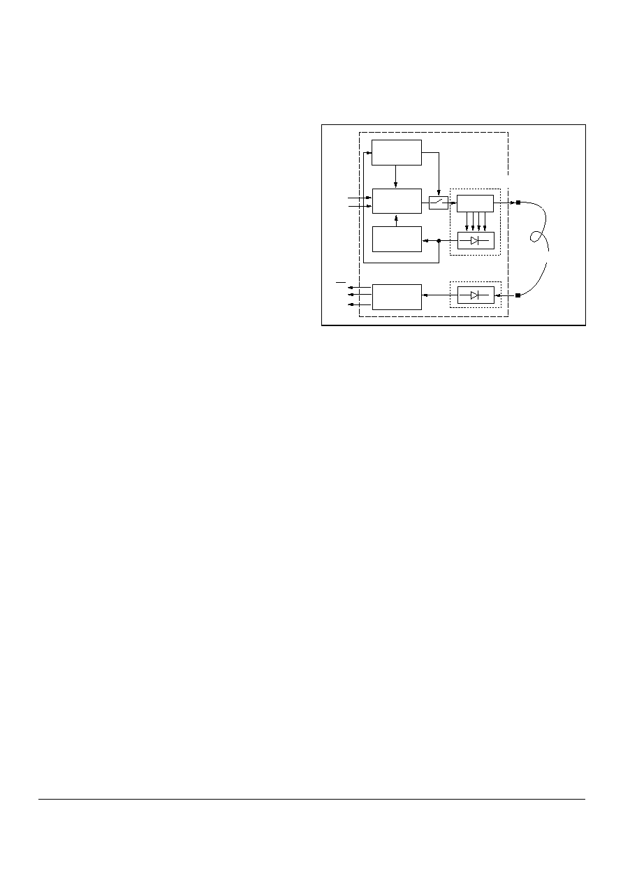
Functional Description
This transceiver is designed to transmit serial data via single
mode cable.
Functional Diagram
The receiver component converts the optical serial data into
PECL compatible electrical data (RD and RDnot). The Signal
Detect (SD, active high) shows whether optical data is
present
(1)
.
The transmitter converts electrical PECL compatible serial data
(TD and TDnot) into optical serial data. It contains a laser driver
circuit that drives the modulation and bias current of the laser
diode. The currents are controlled by a power control circuit to
guarantee constant output power of the laser over temperature
and aging.
The power control uses the output of the monitor PIN diode
(mechanically built in the laser coupling unit) as a controlling sig-
nal, to prevent the laser power from exceeding the operating
limits.
This module is a Class 1 laser product, due to an integrated
automatic shutdown circuit that disables the laser when it
detects transmitter failures.
The transceiver contains a supervisory circuit to monitor the
power supply. This circuit makes an internal reset signal
whenever the supply voltage drops below the reset threshold.
It keeps the reset signal active for at least 140 milliseconds
after the voltage has risen above the reset threshold. During
this time the laser is inactive.
Note
1. We recommend to switch off the transmitter supply (V
CC
-Tx) if no
transmitter input data is applied.
Automatic
Shut-Down
Laser
Driver
Power
Control
Receiver
o/e
o/e
Laser
e/o
RX Coupling Unit
TD
TD
RD
RD
SD
Laser Coupling Unit
Single Mode Fiber
LEN
Monitor
Fiber Optics
V23806-A34-C2, Single Mode FDDI 1x9 Transceiver
3
TECHNICAL DATA
The electro-optical characteristics described in the following
tables are valid only for use under the recommended operating
conditions.
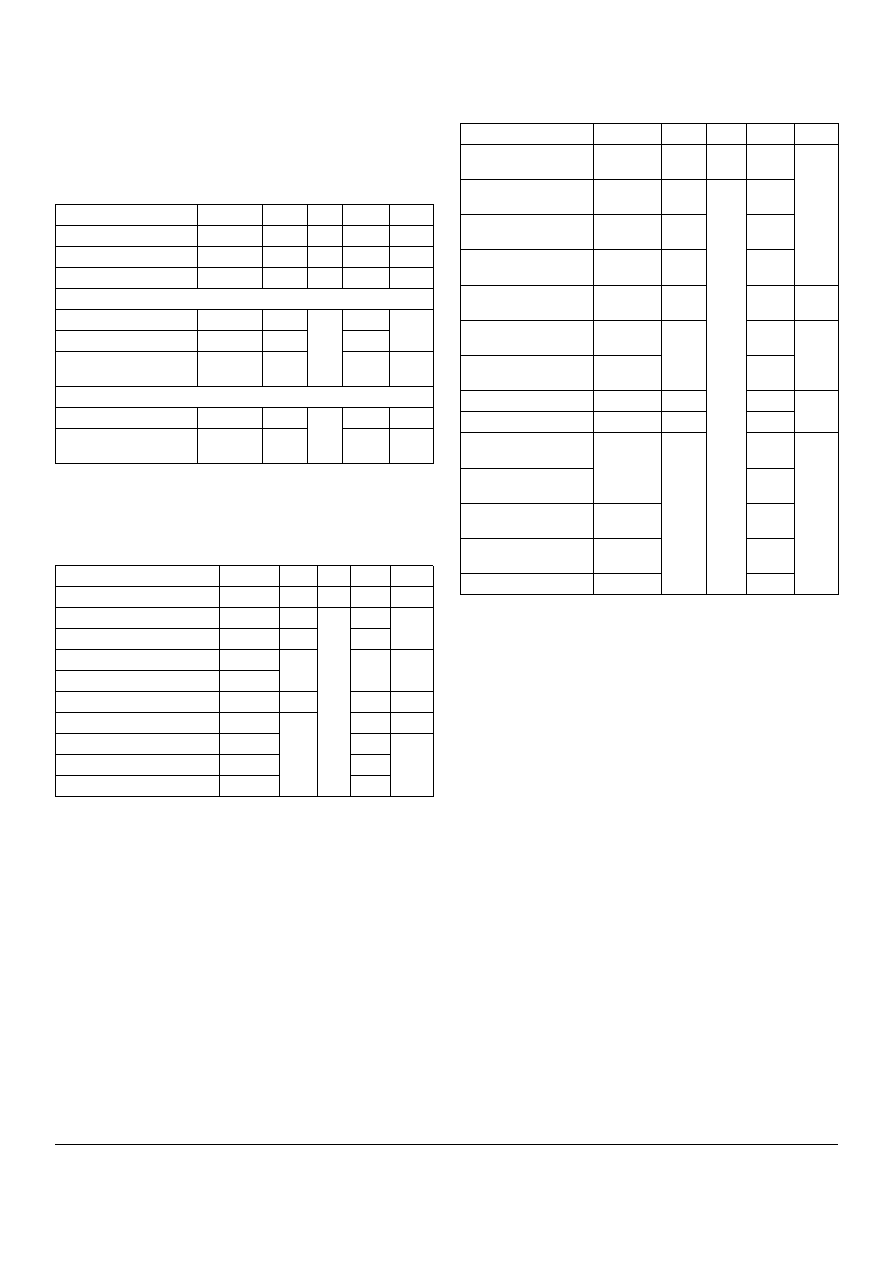
Recommended Operating Conditions
Note
1. For
V
CC
≠V
EE
(min., max.). 50% duty cycle. The supply current does
not include the load drive current of the receiver output. Add max.
45 mA for the three outputs. Load is 50
to V
CC
≠2 V.
Transmitter Electro-Optical Characteristics
Notes
1. Measured at the end of 5 meters of single mode fiber. The FDDI
Halt Line state (12.5 MHz square wave) is used. Specified values are
valid for EOL and over the whole temperature range.
2. The weighted average wavelength of the optical spectrum output.
3. FOTP-127 is used to measure central wavelength and RMS
spectral width.
4. The weighted root mean square (RMS) width of the optical
output spectrum.
5. To 90% (90% to 10%) levels. Measured using the Halt Line state
(12.5 MHz square wave).
6. Measurement done using the Idle Line state (62.5 MHz square
wave).
7. Test method as in PMD Appendix A. All jitter values are peak-to-peak.
8. Measurement done using the Worst Case test pattern described in
the PMD Appendix A.5.
9. Measurement done using the Idle Line state (62.5 MHz square
wave). BER=2.5
≠10
.
Receiver Electro-Optical Characteristics
Notes
1. Minimum average power at which the BER is less than 2.5
≠10
or lower. Measured with the ANSI Worst Case pattern from
Appendix 5 of the PMD.
2. An increase in optical power of data signal above the specified level
will cause the SIGNAL DETECT to switch from a Low state to a High
state.
3. A decrease in optical power of data signal below the specified level
will cause the SIGNAL DETECT to switch from a High state to a Low
state.
4. PECL compatible. Load is 50
into V
CC
≠2 V. Measured under DC
conditions. For dynamic measurements a tolerance of 50 mV should
be added. V
CC
=5 V.
5. PECL compatible. A high level on this output shows that optical data
is applied to the optical input.
6. Measurement done using the Idle Line state (62.5 MHz
square wave).
7. Test method as in PMD Appendix A. All jitter values are peak-
to-peak.
8. Measurement done using the Worst Case test pattern described in
the PMD Appendix A.5.
9. Measurement done using the Idle Line state (62.5 MHz square
wave). BER=2.5
≠10
.
Parameter
Symbol
Min.
Typ. Max.
Units
Ambient Temperature
T
AMB
0
70
∞C
Power Supply Voltage
V
CC
≠V
EE
4.75
5.0
5.25
V
Supply Current
(1)
I
CC
150
250
mA
Transmitter
Data Input High Voltage V
IH
≠V
CC
≠1165
≠880
mV
Data Input Low Voltage V
IL
≠V
CC
≠1810
≠1475
Input Data Rise/Fall
Time, 10%≠90%
t
R
, t
F
0.4
1.3
ns
Receiver
Output Current
I
O
25
mA
Input Center
Wavelength
C
1260
1360
nm
Transmitter Symbol
Min. Typ. Max. Units
Output Power (Average)
(1)
P
O
≠20
≠16
≠14
dBm
Center Wavelength
(2, 3)
l
C
1270
1340 nm
Spectral Width (RMS)
(3, 4)
l
15
Output Rise Time
(5)
t
R
0.6
3.5
ns
Output Fall Time
(5)
t
F
Extinction Ratio (Dynamic)
ER
10
dB
Overshoot
OS
25
%
Duty Cycle Distortion
(6, 7)
DCD
1.0
ns
Data Dependent Jitter
(7, 8)
DDJ
0.6
Random Jitter
(7, 9)
RJ
0.69
Receiver
Symbol
Min.
Typ.
Max.
Units
Sensitivity
(Average Power)
(1)
P
IN
≠33
≠31
dBm
Saturation
(Average Power)
(1)
P
SAT
≠14
Signal Detect
Assert Level
(2)
P
SDA
≠31
Signal Detect
Deassert Level
(3)
P
SDD
≠40.5
≠32.5
Signal Detect
Hysteresis
P
SDA
≠
P
SDD
1
dB
Signal Detect
Assert Time
t
ASS
100
µ
s
Signal Detect
Deassert Time
t
DAS
350
Output Low Voltage
(4)
V
OL
≠V
CC
≠1950
≠1630
mV
Output High Voltage
(4)
V
OH
≠V
CC
≠1025
≠735
Output Data Rise/Fall
Time, 10%≠90%
t
R
, t
F
1.3
ns
Output SD
Rise/Fall Time
(5)
40
Duty Cycle
Distortion
(6, 7)
DCD
0.4
Data Dependent
Jitter
(7, 8)
DDJ
1.0
Random Jitter
(7, 9)
RJ
2.1

Fiber Optics
V23806-A34-C2, Single Mode FDDI 1x9 Transceiver
4
Pin Description
Regulatory Compliance
EYE SAFETY
This laser based single mode transceiver is a Class 1 product. It
complies with IEC 60825-1 and FDA 21 CFR 1040.10 and
1040.11.
To meet laser safety requirements the transceiver shall be oper-
ated within the Absolute Maximum Ratings.
Caution
All adjustments have been made at the factory prior to ship-
ment of the devices. No maintenance or alteration to the
device is required.
Tampering with or modifying the performance of the device
will result in voided product warranty.
Note
Failure to adhere to the above restrictions could result in a modifica-
tion that is considered an act of "manufacturing," and will require,
under law, recertification of the modified product with the U.S. Food
and Drug Administration (ref. 21 CFR 1040.10 (i)).
Laser Data
Required Labels
Laser Emission
Pin Name
Level
Pin # Description
RxV
EE
Rx
Ground Power
Supply
1
Negative power supply,
normally ground
RD
Rx Output
Data
PECL
Output
2
Receiver output data
RDn
Rx Output
Data
PECL
Output
3
Inverted receiver
output data
SD
Rx Signal
Detect
PECL
Output
active
high
4
A high level on this output
shows that optical data is
applied to the optical
input.
RxV
CC
Rx +5 V
Power
Supply
5
Positive power supply,
+5 V
TxV
CC
Tx +5 V
Power
Supply
6
Positive power supply,
+5 V
TDn Tx
Input
Data
PECL
Input
7
Inverted transmitter
input data
TD
Tx Input
Data
PECL
Input
8
Transmitter input data
TxV
EE
Tx
Ground
Power
Supply
9
Negative power supply,
normally ground
Stud Pin
Mech.
Support
S1/2
Stud connected to V
EE
Feature
Standard
Comments
Electrostatic
Discharge (ESD)
to the Electrical
Pins
MIL-STD 883C
Method 3015.4
Class 1 (>1000 V)
Immunity:
Electrostatic
Discharge (ESD)
to the Duplex SC
Receptacle
EN 61000-4-2
IEC 61000-4-2
Discharges of ±15kV
with an air discharge
probe on the receptacle
cause no damage.
Immunity:
Radio Frequency
Electromagnetic
Field
EN 61000-4-3
IEC 61000-4-3
With a field strength of
10 V/m rms, noise
frequency ranges from
10 MHz to 1 GHz. No
effect on transceiver
performance between
the specification limits.
Emission:
Electromagnetic
Interference (EMI)
FCC Class B
EN 55022 Class B
CISPR 22
Noise frequency range:
30 MHz to 1 GHz
Wavelength
1300 nm
Total output power (as defined by IEC: 50 mm
aperture at 10 cm distance)
2 mW
Total output power (as defined by FDA: 7 mm
aperture at 20 cm distance)
180 µW
Beam divergence
4∞
Class 1 Laser Product
IEC
Complies with 21 CFR
1040.10 and 1040.11
FDA
Indication of laser
aperture and beam

Published by Infineon Technologies AG
©
Infineon Technologies AG 1999
All Rights Reserved
Attention please!
The information herein is given to describe certain components and shall not be
considered as warranted characteristics.
Terms of delivery and rights to technical change reserved.
We hereby disclaim any and all warranties, including but not limited to warranties
of non-infringement, regarding circuits, descriptions and charts stated herein.
Infineon Technologies is an approved CECC manufacturer.
Information
For further information on technology, delivery terms and conditions and prices
please contact the Infineon Technologies offices or our Infineon Technologies
Representatives worldwide - see our webpage at
www.infineon.com/fiberoptics
Warnings
Due to technical requirements components may contain dangerous substances.
For information on the types in question please contact your Infineon Technologies
offices.
Infineon Technologies Components may only be used in life-support devices or
systems with the express written approval of Infineon Technologies, if a failure of
such components can reasonably be expected to cause the failure of that
life-support device or system, or to affect the safety or effectiveness of that device
or system. Life support devices or systems are intended to be implanted in the
human body, or to support and/or maintain and sustain and/or protect human life.
If they fail, it is reasonable to assume that the health of the user or other persons
may be endangered.
Infineon Technologies AG ∑ Fiber Optics ∑ Wernerwerkdamm 16 ∑ Berlin D-13623, Germany
Infineon Technologies, Inc. ∑ Fiber Optics ∑ 1730 North First Street ∑ San Jose, CA 95112, USA
Infineon Technologies K.K. ∑ Fiber Optics ∑ Takanawa Park Tower ∑ 20-14, Higashi-Gotanda, 3-chome, Shinagawa-ku ∑ Tokyo 141, Japan
APPLICATION NOTE
Single Mode 1x9 Transceiver
* Recommended choke is Siemens Matsushita B78108-S1153-K or B78148-S1153-K (Q
min
=60, max. DC resistance=0.6
).
The power supply filtering is recommended for good EMI per-
formance. Use short tracks from the inductor L1/L2 to the mod-
ule V
CC
≠RX/V
CC
≠TX. We recommend a V
EE
plane under the
module for getting good EMI and sensitivity performance.
Studs should be connected to this V
EE
plane. The transceiver
contains an automatic shutdown circuit.
Reset is only possible if the power is turned off, and then on
again. V
CC
TX switched below V
TH
. Further application notes for
electrical interfacing are available upon request. Ask for App-
note 82.
Application board available on request.
V
EE
TxD
TxDN
R2
R4
1
27R
1
27R
S2
S1
Top View
Transceiver
R9
R8
R6
1
27R
1
27R
51
0R
V
EE
V
EE
V
EE
V
EE
RxD
RxDN
SD
V
EE
V
EE
V
EE
V
EE
V
EE
V
EE
C3
C4
V
CC
C2
C1
R1
R3
V
CC
R5
R7
82R
82R
82R
82R
V
CC
-Tx
V
CC
-Rx
L1
L2
9
1
RxV
EE
TxV
EE
DC coupling between ECL gates
R1/3/5/7 = 82
R2/4/6/8 = 127
R9 = 510
C1/3 = 4.7 µF
C2/4 = 4.7 µF
L1/2 = 15 µH (L2 optional)*