
Fiber Optics
JULY 1999
V23809-F7-C10
Multimode 1300 nm LED Fibre Channel
266 MBd Transceiver*
FEATURES
∑ Fully compliant with all major standards
∑ Compact integrated transceiver unit with duplex SC
receptacle
∑ Single power supply with 3.0 V to 5.5 V range
∑ Extremely low power consumption < 0.7 W at 3.3 V
∑ PECL differential inputs and outputs
∑ System is optimized for 62.5/50
µ
m graded index fiber
∑ Industry standard multisource footprint
∑ Very low profile for high slot density
∑ Process plug included
∑ Wave solderable and washable with process
plug inserted
∑ Testboard available
∑ UL-94 V-0 certified
* Available also as FC 133 MBd V23809-B7-C10 on request
APPLICATIONS
∑ FC fabric point-to-point links
∑ HIPPI, SCSI, IPI
∑ High speed computer links
∑ Local area networks up
to 320 MBd
∑ High definition digital television
∑ Switching systems
Absolute Maximum Ratings
Exceeding any one of these values may destroy the device
immediately.
Supply Voltage (V
CC
≠V
EE
) .......................................... ≠0.5 to 7 V
Data Input Levels (PECL) (V
IN
) .................................. V
EE
to V
CC
Differential Data Input Voltage (
V
IN
).................................. 3.0 V
Operating Ambient Temperature (T
AMB
) .................0
∞
C to 85
∞
C
Storage Ambient Temperature (T
STG
).................. ≠40
∞
C to 85
∞
C
Humidity/Temperature Test Condition (R
H
)................. 85%/85
∞
C
Soldering Conditions, Temp/Time (T
SOLD
/t
SOLD
)
(MIL-STD 883C, Method 2003) .............................. 270
∞
C/10 s
ESD Resistance (all pins to V
EE
, human body) .................. 1.5 kV
Output Current (I
O
) ........................................................... 50 mA
Dimensions in (mm) inches
(1
±
0.1
)
.04
±
.039
(0.7
±
0.1
)
.028
±
.004
5.2
.205
Optical
Centerline
PC board
(10 max)
.393 max
(
3
±
0.2
)
.118
±
.008
(2) .080
12.7
.500
(0.63
±
0.2
)
.025
±
.008
(25.25
±
0.05
)
.994
±
.002
8x 2.54=20.32
8x .100 =.800
123456789
20.32
.800
(15.88
±
0.5
)
.625
±
.020
(38.6
±
0.15
)
1.52
±
.006
(11 max)
.433 max
0.1
M
.004
M
0.3
M
.012
M
A
A
0.3
M
.012
M
A
A
11x
2x
(1.4
≠0.05
)
.055
≠.002
Z
9x
DUPLEX
SC
RECEPTACLE
View Z
(Lead cross section
and standoff size)
Rx
Tx
(2.8 max)
.110 max
8x 2.54=20.32
8x .100 =.800
20.32
.800
(2.54)
.100
9x
(0.8
±
0.1
)
.031
±
.004
0.1
M
.004
M
11x
(1.9
±
0.1
)
.075
±
.004
2x
(2.54)
.100
(0.6
±
0.1
)
.024
±
.004
(8.6 max)
.170 max
(3.8 max)
.150 max
(0.3
±
0.02
)
.012
±
.001
Top view
PC board
thickness
Footprint
A

Semiconductor Group
V23809-F7-C10, Multimode 1300 nm LED Fibre Channel 266 MBd Transceiver
2
DESCRIPTION
This data sheet describes the Infineon Fibre Channel trans-
ceiver, which belongs to the Infineon Multistandard Transceiver
Family. It is fully compliant with the Fibre Channel FC-133
MBaud and FC-266 MBaud draft standard.
Fibre Channel provides a general transport for upper layer proto-
cols such as Intelligent Peripheral Interface (IPI), High Perfor-
mance Parallel Interface (HIPPI) and Small Computer System
Interface (SCSI) command sets. Defined transmission rates are
266 MBaud and 133 MBaud in point-to-point or fabric topology.
The Infineon low cost multistandard transceiver is a single unit
comprised of a transmitter, a receiver, and an SC receptacle.
This design frees the customer from many alignment and
PC board layout concerns. The modules are designed for low
cost applications.
The inputs/outputs are PECL compatible, and the unit operates
from a 3.0 V to 5.5 V power supply. As an option, the data out-
put stages can be switched to static levels during absence of
light as indicated by the Signal Detect function. It can be
directly interfaced with available chipsets.
Regulatory Compliance
TECHNICAL DATA
The electro-optical characteristics described in the following
tables are valid only for use under the recommended operating
conditions.
Recommended Operating Conditions
Notes
1. For
V
CC
≠V
EE
(min., max.). 50% duty cycle. The supply current
(I
CC2
+I
CC3
) does not include the load drive current (ICC1). Add max.
45 mA for the three outputs. Load is 50
to V
CC
≠2 V.
2. To maintain good LED reliability, the device should not be held in the
ON state for more than the specified time. Normal operation should
be done with 50% duty cycle.
3. To achieve proper PECL output levels the 50
termination should
be done to V
CC
≠2 V. For proper termination see the application
notes.
Feature
Standard
Comments
Electromagnetic
Interference (EMI)
FCC Class B
EN 55022 Class B
CISPR 22
Noise frequency
range:30 MHz to
1 GHz
Immunity:
Electrostatic
Discharge
EN 61000-4-2
IEC 1000-4-2
Discharges of
±
15kV with an air
discharge probe on
the receptacle cause
no damage.
Immunity:
Radio Frequency
Electromagnetic
Field
EN 61000-4-3
IEC 1000-4-3
With a field strength
of 10 V/m rms, noise
frequency ranges
from 10 MHz to
1 GHz
Eye Safety
IEC 825-1
Class 1
Parameter
Symbol
Min.
Typ. Max.
Units
Ambient Temperature
T
AMB
0
70
∞
C
Power Supply Voltage V
CC
≠V
EE
3
5.5
V
Supply Current 3.3 V
I
CC
230
mA
Supply Current 5 V
(1)
260
Transmitter
Data Input
High Voltage
V
IH
≠V
CC
≠1165
≠880
mV
Data Input
Low Voltage
V
IL
≠V
CC
≠1810
≠1475
Threshold Voltage
V
BB
≠V
CC
≠1380
≠1260
Input Data Rise/Fall
Time, 20%≠80%
t
R
, t
F
0.4
1.3
ns
Data High Time
(2)
t
ON
1000
Receiver
Output Current
I
O
25
mA
Input Duty Cycle
Distortion
t
DCD
1
ns
Input Data
Dependent Jitter
t
DDJ
1
Input Random Jitter
t
RJ
0.76
Input Center
Wavelength
C
1260
1380
nm
Electrical
Output Load
(3)
R
L
50
Fiber Optics
V23809-F7-C10, Multimode 1300 nm LED Fibre Channel 266 MBd Transceiver
3
Transmitter Electro-Optical Characteristics
(Values in brackets are for 320 MBd)
Notes
1. Measured at the end of 5 meters of 62.5/125/0.275 graded index
fiber using calibrated power meter and a precision test ferrule.
Cladding modes are removed. Values valid for EOL.
2. The input data pattern is a 12.5 MHz square wave pattern.
3. Center wavelength is defined as the midpoint between the two
50% levels of the optical spectrum of the LED.
4. Spectral width (full width, half max.) is defined as the difference
between 50% levels of the optical spectrum of the LED.
5. 10% to 90% levels. Measured using a 12.5 MHz square wave pat-
tern with an optoelectronic measurement system (detector and
oscilloscope) with 3 dB bandwidth ranging from less than 0.1 MHz
to more than 750 MHz.
6. Extinction ratio is defined as PL/PH x 100%. Measurement system
as in Note 5.
7. Test method and consideration as in FC-PH Appendix A.
8. Measured with the K28.5 pattern from Chapter II of the FC-PH
at 266MBd.
9. Measured with the K28.7 pattern from Chapter II of the FC-PH
which equals a 133 MHz square wave.
Receiver Electro-Optical Characteristics
(Values in brackets are for 320 MBd)
Notes
1. Pattern: Manchester coding / NRZI (no scrambling)
2. For a bit error rate (BER) of less than 1x10E-12 over a receiver eye
opening of least 1.0ns. Measured with a 2
7
≠1 PRBS.
3. For a BER of less than 1x10E-12. Measured in the center of the eye
opening with a 2
7
≠1 PRBS.
4. Test method and considerations as in FH-PC Appendix A.
5. Measured with the K28.5 pattern from Chapter II of the FC-PH at
266 MBd.
6. Measured with the K28.7 pattern from Chapter II of the FC-PH
which equals a 133 MHz square wave.
7. An increase in optical power through the specified level will cause
the Signal Detect output to switch from a Low state to a High state.
8. A decrease in optical power through the specified level will cause
the Signal Detect output to switch from a High state to a Low state.
9. PECL compatible. Load is 50
into V
CC
≠2 V. Measured under DC
conditions. For dynamic measurements a tolerance of 50 mV should
be added for V
CC
=5 V.
Transmitter Symbol Min.
Typ.
Max. Units
Data Rate
DR
0
266
(320)
mBaud
Launched Power
(Average)
(1, 2)
into 62.5
µ
m Fiber
P
O
≠20
(≠21)
≠16
(≠17)
≠14
dBm
Center Wavelength
(2, 3)
C
1280
1380 nm
Spectral Width
(FWHM)
(2, 4)
l
200
Output Rise Time,
10%≠90%
(5)
t
R
0.6
2.0
(2.5)
ns
Output Rise Time,
10%≠90%
(5)
t
F
2.2
(2.5)
Temperature Coefficient
of Optical Output Power
TCp
.03
dB/
∞
C
Extinction Ratio
(Dynamic)
(2, 6)
ER
12
%
Deterministic Jitter
(7, 8)
t
DJ
16
Random Jitter
(7, 9)
t
RJ
9
Receiver
Symbol
Min.
Typ.
Max.
Units
Data Rate
DR
5
(1)
266
(320)
mBaud
Sensitivity
(Average Power)
(2)
P
IN
≠30
≠26
dBm
Saturation
(Average Power)
(3)
P
SAT
≠14
≠11
Deterministic
Jitter
(4, 5)
t
DJ
19
%
Random Jitter
(4, 6)
t
RJ
9
Signal Detect
Assert Level
(7)
P
SDA
≠43.5
≠29
dBm
Signal Detect
Deassert Level
(8)
P
SDD
≠45
≠30.5
Signal Detect
Hysteresis
P
SDA
≠
P
SDD
1.5
dB
Output Low
Voltage
(9)
V
OL
≠V
CC
≠1810
≠1620 mV
Output High
Voltage
(9)
V
OH
≠V
CC
≠1025
≠880
Output Data Rise/Fall
Time, 20%≠80%
t
R
, t
F
1.3
ns
Output SD Rise/Fall
Time, 20%≠80%
40
Fiber Optics
V23809-F7-C10, Multimode 1300 nm LED Fibre Channel 266 MBd Transceiver
4
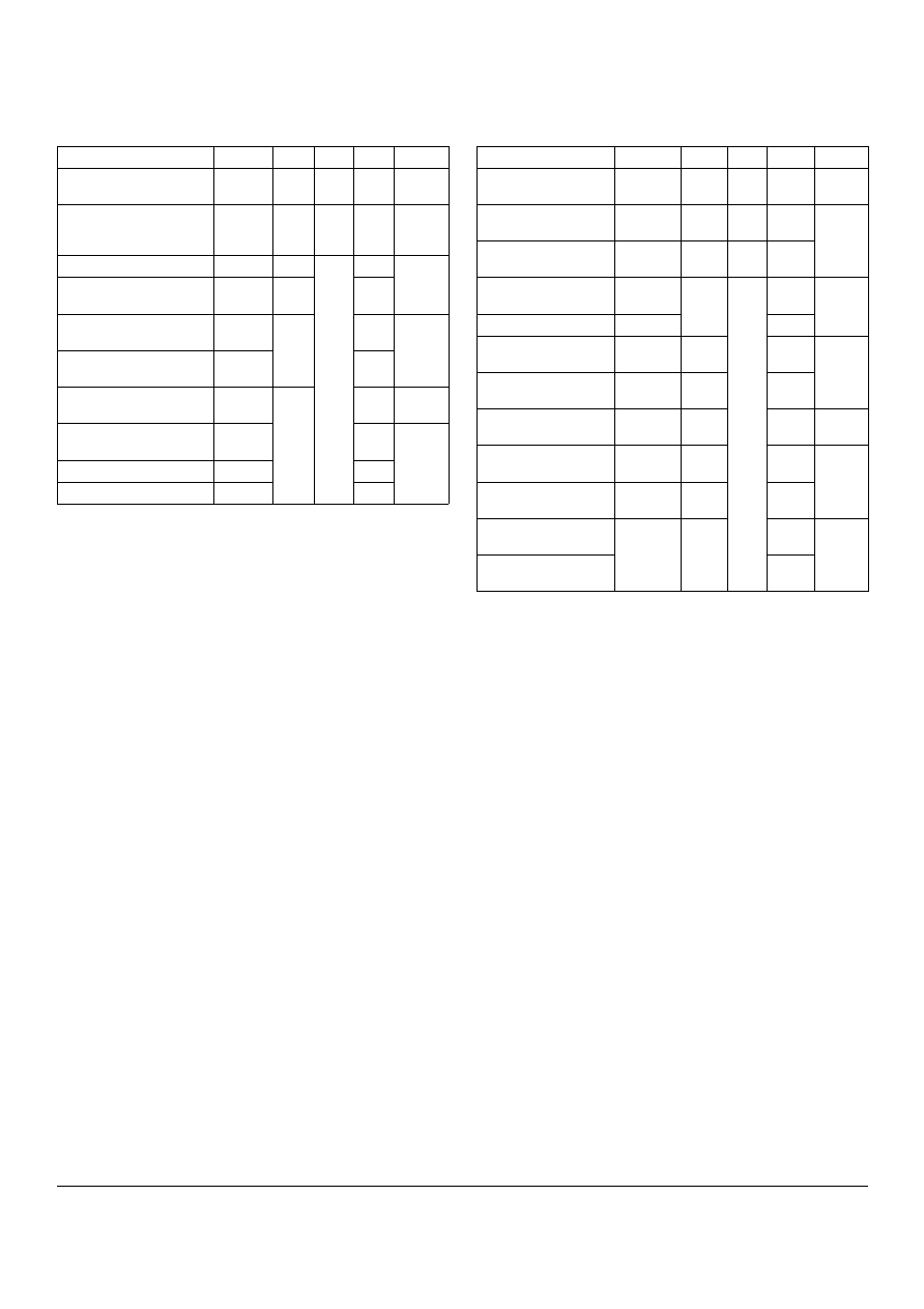
Pin Description for 1x9 Pin Row
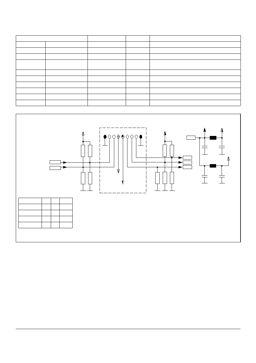
APPLICATION NOTE FOR 1X9 PIN ROW TRANSCEIVER
The power supply filtering is required for good EMI perfor-
mance. Use short tracks from the inductor L1/L2 to the module
V
CC
≠RX/V
CC
≠TX.
A GND plane under the module is recommended for good EMI
and sensitivity performance.
Pin Name
Level
Pin #
Description
RxV
EE
Rx Ground
Power Supply
1
Negative power supply, normally ground
RxD
Rx Output Data
PECL Output
2
Receiver output data
RxDn
Rx Output Data
PECL Output
3
Inverted receiver output data
Rx SD
RX Signal Detect
PECL Output
active high
4
A high level on this output shows that an optical signal
is applied to the optical input
RxV
CC
Rx +3.3...5 V
Power Supply
5
Positive power supply, +3.3...5 V
TxV
CC
Tx +3.3...5 V
Power Supply
6
Positive power supply, +3.3...5 V
TxDn
Tx Input Data
PECL Input
7
Inverted transmitter input data
TxD
Tx Input Data
PECL Input
8
Transmitter input data
TxV
EE
Tx Ground
Power Supply
9
Negative power supply, normally ground
Case
Support
Not Connected
S1/S2
Support stud, not connected
GND
C1
VCC
VCC
GND
C2
VCC≠RX
L1
GND
C3
GND
C4
L2
VCC≠TX
GND
GND
VCC-TX
VCC-RX
Transceiver
GND GND
R3
R1
VCC≠TX
GND GND
R7
R5
VCC≠RX
200R
GND
R9
R8
R6
RD
RDN
SD
TXD
TXDN
R2
R4
9
1
C1/3=4700 nF (optional)
C2/4=4700 nF
L1/2=15000 nH (L2 is optional)
R9=200 Ohm
R in OHM
5 V 4 V 3.3 V
R1/3
82
100 127
R2/4
130 100 83
R5/7
82
100 127
R6/8
130 100 83
DC coupling between ECL gates.

Infineon Technologies AG i. Gr. ∑ Fiber Optics ∑ Wernerwerkdamm 16 ∑ Berlin D-13623, Germany
Infineon Technologies, Corp. ∑ Fiber Optics ∑ 19000 Homestead Road ∑ Cupertino, CA 95014 USA
Siemens K.K. ∑ Fiber Optics ∑ Takanawa Park Tower ∑ 20-14, Higashi-Gotanda, 3-chome, Shinagawa-ku ∑ Tokyo 141, Japan
www.infineon.com/fiberoptics
APPLICATION NOTE FOR MULTIMODE 1300 NM LED TRANSCEIVER
Solutions for connecting a Infineon 3.3 V Fiber Optic Transceiver to a 5.0 V Framer-/Phy-Device.
Figure 1. Common GND
Figure 2. Common V
CC
Framer/Phy
Clock
Recovery
Infineon
Fiber
Optic
Transceiver
V
CC
V
CC
Data
In
Data
Out
SD
In
Rx
Out
Tx
In
SD
Out
50
0
83
50
0
68
12
7
18
0
V
CC
5.0 V
V
CC
3.3 V
100 nF
100 nF
Framer/Phy
Clock
Recovery
5V
Infineon
Fiber
Optic 3.3 V
Transceiver
V
CC
V
CC
SD
In
51
0
18
K
V
CC
5.0 V
V
CC
3.3 V
SD
Out
1
1
1.8 V
Zener-Diode 1.8 V
Framer/Phy
Clock
Recovery
5V
Infineon
Fiber
Optic 3.3 V
Transceiver
V
CC
V
CC
SD
83
39K
127
26K
V
CC
5.0 V
V
CC
3.3 V
SD
SD
Inputs and outputs are differential and should be
doubled. Signal Detect (SD) is single ended (if used).
Figure 1a. Circuitry for SD (Differential) and
Common GND
Figure 1b. Circuitry for SD (Single Ended)
and Common GND
Framer/Phy
Clock
Recovery
Infineon
Fiber
Optic
Transceiver
V
CC
V
CC
Data
In
Data
Out
SD
In
Rx
Out
Tx
In
SD
Out
V
CC
GND 5.0 V
GND 5.0 V
GND 3.3 V
GND 3.3 V
GND 3.3 V
20
0
82
83
1
2
7
13
0
Inputs and outputs are differential
and should be doubled. Signal
Detect (SD) is single ended.