
Fiber Optics
SEPTEMBER 1999-1
V23816-N1018-C23
Single Mode 1310 nm 16-Line Parallel 2.5 GBd Transceiver
OC-48 SONET / SDH Telecom Links up to 15 km
Preliminary
FEATURES
∑ Compliant with existing standards
∑ Compact integrated transceiver unit with
≠ DFB laser diode transmitter
≠ InGaAs PIN photodiode receiver
≠ Pigtailed optical connections
≠ Integrated Mux, Demux and Clock Recovery
∑ Class 1 FDA and IEC laser safety compliant
∑ Dual power supply (+3.3 V, +5 V)
∑ OC-48 optical transmit and receive at 2488.32 Mbit/s
∑ LVPECL (+3.3 V) Single Ended 16-line parallel interface at
155.52 Mbit/s
∑ External control for laser shutoff
∑ Loss of optical signal and Loss of synch indicators (Rx)
∑ Loss of lock indicator for TX high speed clock
∑ Laser bias monitor
Absolute Maximum Ratings
Exceeding any one of these values may destroy the device
immediately.
PECL Supply Voltage (V
CC
PECL
)................................... 0 to 5.5 V
LVPECL Supply Voltage (V
CC
LVPECL
) ............................... 0 to 5 V
LVPECL Data and Clock Input Levels................... 0 to V
CC
LVPECL
LVPECL Data and Clock Output Source Current............... 50 mA
Operating Ambient Temperature
(1)
.............................. 0 to 70∞C
Storage Ambient Temperature
................................ ≠
40 to +85∞C
Static Discharge Voltage, All Pins .................................... 1000 V
Input Common Mode Noise on Supply Lines
(2)
......... 50 mV p-p
Notes
1. Operating ambient temperature with 200 lfm airflow across the
transceiver. In the case of convection cooling, the operating ambient
temperature is specified to be 0 to +50∞C.
2. 6 KHz to 2 MHz
Dimensions in (mm) inches
(0.435)
.013
(22.86)
.9
(88.9
±
0.5
)
3.5
±
.02
Bottom view
Rx
Tx
35.56
1.4
57.15
2.25
(63.5
±
0.5
)
2.5
±
0.02
(570
±
25)
22.44
±
1
(4.64)
.183
69.85
2.75
(57.15)
2.25
Top side
a
(
3.2
±
0.12)
.126
±
.005
(53.48
±
0.03)
2.106
±
.001
dia.078+.003)
1.98+0.08
(15.88
±
0.5)
.625
±
.02
(1)
.04
(10.16
±
0.25)
.4
±
.01
(13.72
±
0.5)
.54
±
.02
4x
b
c
c
Pin 99
Pin 100
Pin 1
Pin 2
4
c
c
Top side

Fiber Optics
V23816-N1018-C23, SM 1310nm 2.5GBd Trx OC-48 SONET/SDH Telecom Links,15km
2
DESCRIPTION
The Infineon single mode SONET/SDH transceiver is compliant
with the Bellcore GR-253, ITU-T G.957 and ITU-T G.958 specifi-
cations. The transmitter section consists of a multiplexer, laser
driver, DFB laser diode and pigtail single mode fiber. The
receiver section consists of a multimode fiber pigtail, PIN pho-
todiode / preamplifier, postamplifier, clock and data recovery
unit and a demultiplexer. The 155 Mb/s parallel data interface
frees the customer from the concerns of pcb layout at 2.5 Gb/s.
The pluggable connector mates easily to the customer pcb, and
allows the transceiver to be removed prior to any solder reflow
or washing of the customer pcb.
The transceiver operates from a dual power supply (+3.3 V and
+5 V). The transceiver electrical interface is via a 100 pin plugga-
ble connector pair. The transmit and receive electrical signals
each consist of 16 parallel single-ended data lines which are
LVPECL (+3.3 V) compatible, and a differential LVPECL clock.
Both the transmit input data and clock lines, and the receive
outputs data and clock lines, are internally biased and termi-
nated. All lines are DC coupled to the interface connector.
Functional Description
This transceiver is designed to transmit and receive serial
2.5 Gb/s data via singlemode fiber at 1310 nm wavelength.
The transmitter accepts 16 lines of parallel electrical data at
155.52 Mb/s and a synchronous transmit clock at 155.52 MHz.
The data should be updated on the rising edge of the positive
transmit clock (TxDI55P). The data is multiplexed into a serial
data stream at 2488.32 Mbit/s. The data follows the SONET bit
ordering, where the MSB (Bit 0) is transmitted first, and the
LSB (Bit 15) is transmitted last. The laser driver circuit drives the
modulation and bias currents of the laser diode. The 2488.32
Mbit/s optical data stream is transmitted at 1310 nm wave-
length. The laser bias current is controlled by a power control
circuit, which regulates the output power over temperature and
aging. This is accomplished by using the output of a monitor
PIN diode (mechanically built into the laser unit) as a feedback
signal to prevent the laser power from exceeding the operating
limits. The laser driver modulation current is temperature com-
pensated to ensure a constant extinction ratio over temperature
variations.
The laser can be switched off with a logical low signal on the
Laser Shutoff input. The input is internally pulled high, so it can
be driven with an open collector TTL interface. The laser bias
current is monitored as an analog output voltage at the Bias
Monitor output (IB) pin. The bias monitor can be used to moni-
tor the aging of the laser.
The receiver accepts an input serial optical data stream at
2488.32 Mbit/s. The PIN/Preamp detects the incoming light and
converts it to an electrical current, which is then amplified. The
Clock and Data Recovery unit recovers the clock from the input
data stream, and aligns the data so it is synchronous with the
clock. The data is then demultiplexed directly to 16 lines of par-
allel data at 155.52 Mbit/s, with the MSB being Bit 0 and the
LSB being Bit 15. The receiver also outputs a 155.52 MHz syn-
chronous clock. The received data is updated on the falling
edge of the positive receive clock (RxQI55P).
The Rx Alarm (FLAG) indicator will switch active low if there is a
loss of optical input signal (LOS) or if the PLL in the clock recov-
ery unit is unlocked (Lock). The FLAG output is an open collec-
tor TTL, and can be used to monitor the function of the receiver.
TECHNICAL DATA
The electro-optical characteristics described in the following
tables are only valid for use under the recommended operating
conditions.
Recommended Operating Conditions
Parameter
Symbol
Min.
Typ.
Max.
Units
Operating Am-
bient Tempera-
ture
(1)
T
AMB
0
70
∞C
Supply Voltage
5 V PECL
V
CC
PECL
4.75
5.0
5.25
V
Supply Voltage
3.3 V LVPECL
V
CC
LVPECL
3.04
3.3
3.46
Supply Current
5 V PECL
I
CC
PECL
350
Tbd
mA
Supply Current
3.3 V LVPECL
I
CC
LVPECL
1270
Tbd
Total Power
Consumption
P
TOT
6.0
Tbd
W
Transmitter
Data Input Bit
Rate
155.52
Mbit/s
Clock Input
Frequency
155.52
MHz
Clock Input
Frequency
Tolerance
≠100
100
ppm
Clock Input
Duty Cycle
40
50
60
%
Clock Input Jit-
ter Tolerance,
10 Hz to 20
MHz
UI, rms
0.1
rms
UI, p-p
1
p-p
Clock Input
Return Loss,
10 MHz to 700
MHz
20
dB
Data Input
Return Loss,
10 MHz to
700
MHz
15
dB
Clock and Data
Input
High Voltage
(2)
V
CC
LVPECL
≠1.165
V
CC
LVPECL
≠0.88
V
Clock and Data
Input Low
Voltage
(2)
V
CC
LVPECL
≠2
V
CC
LVPECL
≠1.475
Clock Input Dif-
fential Swing
0.3
1.3
V p-p
Data Input
Single Ended
Swing
(3)
0.15
0.6
Input Clock and
Data Rise/Fall
Time
10%≠90%
t
R
, t
F
1.5
ns
Fiber Optics
V23816-N1018-C23, SM 1310nm 2.5GBd Trx OC-48 SONET/SDH Telecom Links,15km
3
Recommended Operating Conditions - continued
Notes
1. Operating ambient temperature with 200 lfm airflow across the
transceiver. In the case of convection cooling, the operating ambient
temperature is specified to be 0 to +50∞C.
2. Tx Clock and Tx Data inputs are DC coupled and internally biased
and terminated.
3. Tx Clock input is differential LVPECL. Tx Data inputs are single ended
LVPECL.
4. The Laser Shutoff input is pulled high internally to VCC
LVPECL
(+3.3 V) through a 1 K resistor.
5. The Tx Lock Detect output is open collector TTL.
6. Measured with 50
to VCC
LVPECL
-2 V. The Rx Clock and Data out-
puts are DC coupled.
7. Rx Clock output is differential LVPECL. Rx Data outputs are single
ended LVPECL.
8. The Rx FLAG output is open collector TTL.
AC Electrical Characteristics
Notes
1. Transmitter input data leading the rising edge of transmit clock posi-
tive (TxDI55P).
2. Transmitter input data lagging the rising edge of transmit clock posi-
tive (TxDI55P).
3. Receiver output data propogation delay with respect to the falling
edge of the positive receive output clock (RxQI55P).
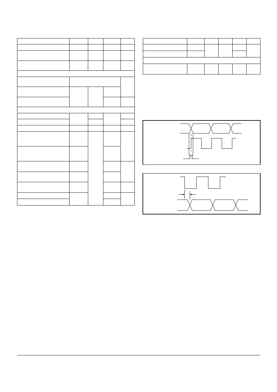
Transmitter Input Timing Diagram
Receiver Output Timing Diagram
Parameter
Min.
Typ.
Max.
Units
Laser Shutoff Delay Time
3
µs
Laser Bias Monitor Transfer
Constant
19
20
21
mV/
mA
Laser Bias Monitor Output
Current
10
mA
Transceiver
Lock Detect Output High
Voltage
(5)
TTL open collector
V
Lock Detect Output Low
Voltage
0.3
Lock Detect Output Current
(Sink)
(5)
200
mA
Receiver
Data Output Bit Rate
155.52
Mbit/s
Clock Output Frequency
155.52
MHz
Clock Output Duty Cycle
45
50
55
%
Clock and Data Output High
Voltage
(6)
V
CC
LVPECL
≠1.15
V
CC
LVPECL
≠0.65
V
Clock and Data Output Low
Voltage
(6)
V
CC
LVPECL
≠2.2
V
CC
LVPECL
≠1.75
Clock Output Diffential
Swing
(7)
0.6
1.3
V p-p
Data Output Single Ended
Swing
(7)
0.3
0.8
Output Clock & Data Rise/
Fall Time 10%≠90%
0.5
1.5
ns
FLAG Output High Voltage
(8)
V
FLAG Output Low Voltage
0.3
Transmitter
Symbol Min.
Typ.
Max.
Units
Data Input Lead Time
(1)
Tlead
1.0
ns
Data Input Lag Time
(2)
Tlag
1.0
Receiver
Data Output
Propogation Delay
(3)
Tpd
≠1
1
ns
Tlead
Tlag
TXD(0..15)
TXD155P
Tpd
RXQ155P
RXQ(0..15)

Fiber Optics
V23816-N1018-C23, SM 1310nm 2.5GBd Trx OC-48 SONET/SDH Telecom Links,15km
4
Transmitter Electro-Optical Characteristics
Notes
1. The transmitter contains a control circuit which regulates the aver-
age optical output power. Nominal output power can be factory set
to any value within the specified range.
2. The Eye Diagram is compliant with Bellcore GR-253 and ITU-T G.957
specifications.
3. Jitter Generation is compliant with GR-253 and ITU-T G.958 specifi-
cations, when measured using a high pass filter with 12 KHz cutoff
frequency, and with a jitter level on the Tx Clock input which is less
than the Jitter Tolerance levels specified in "Transmitter - Recom-
mended Operating Conditions".
4. If the +3.3 V LVPECL Tx power supply drops below the specified
level, the laser bias and modulation currents will be held disabled
until the supply voltage rises above threshold, and after the Power
On Delay Time period.
5. A fault, such as high laser bias current or high average power, which
lasts longer than the specified Fault Delay time, will cause the trans-
mitter to be disabled. Cycling of DC power is then required to reset
the transceiver.
Receiver Electro-Optical Characteristics
Notes
1. Average Rx power for a 1x10
-10
BER, and using a PRBS pattern of
2
23
-1 length with 72 zeros and 72 ones inserted as per ITU-T G.958.
2. Jitter Tolerance for a 1 dB power penalty is defined to be 15 UI from
10 Hz to 600 Hz, 1.5 UI from 6 KHz to 100 KHz, and 0.15 UI from
1 MHz onwards, per ITU-T G.958.
3. Jitter Transfer is defined to be less than 0.1 dB up to 2 MHz, and
dropping at -20 dB/Decade after that point, per ITU-T G.958.
4. The Rx FLAG output is an active low, open collector TTL output,
which is set low if there is a loss of Rx optical signal input (LOS), or if
the clock recovery unit is unable to lock onto the Rx data input. A
decrease in optical input power below the assert level will cause the
FLAG output to switch Low (ON).
Regulatory Compliance
Transmitter
Symbol Min.
Typ.
Max. Units
Nominal Center
Wavelength
NOM
1310
nm
Center Wavelength
Variation
MIN-
MAX
1265
1360
Spectral Bandwidth
20
1
nm
rms
Average Output Power
(1)
P
AVG
≠5
≠2
0
dBm
Extinction Ratio
ER
8.2
dB
Output Rise Time,
20%-80%
T
R
200
ps
Output Fall Time,
80%-20%
T
F
300
Eye Diagram
(2)
ED
Jitter Generation
(3)
J
GEN
0.01
UI rms
Reset Threshold for
V
CC
LVPECL
(4)
V
TH
2.2
2.95
V
Power on delay for
V
CC
LVPECL
(4)
T
POD
20
ms
Fault Delay
(5)
T
FAULT
20
Receiver
Symbol
Min.
Typ.
Max.
Units
Nominal Center Wave-
length
NOM
1310
nm
Sensitivity (Average
Power)
(1)
P
IN
≠22
≠18
dBm
Overload (Average
Power)
(1)
P
OL
0
Optical Return Loss
RL
RX
27
dB
Jitter Tolerance
(2)
J
TOL
Jitter Transfer
(3)
J
XFR
Optical Path Penalty
P
PEN
1
d
Clock Recovery
Acquisition Lock Time
T
LOCK
16
µs
FLAG Output LOS
Assert Level
(4)
P
ASSERT
≠28
≠22
dBm
FLAG Output LOS
Hysteresis
P
HYST
0.5
1
dB
FLAG Output LOS
Assert Time
T
ASSERT
100
µs
Feature
Standard
Comments
Electrostatic
Discharge (ESD)
to the Electrical Pins
MIL-STD 883C
Method 3015.4
Class 1 (>1000 V)
Immunity:
Electrostatic
Discharge (ESD)
to the Connector
EN 61000-4-2
IEC 1000-4-2
Discharges of
±
15kV
with an air discharge
probe on the receptacle
cause no damage.
Immunity:
Radio Frequency
Electromagnetic
Field
EN 61000-4-3
IEC 1000-4-3
With a field strength of
10 V/m rms, noise
frequency ranges from
10 MHz to 1 GHz. No
effect on transceiver
performance between
the specification limits.
Emission:
Electromagnetic
Interference (EMI)
FCC Class B
EN 55022 Class B
CISPR 22
Noise frequency range:
30 MHz to 1 GHz

Fiber Optics
V23816-N1018-C23, SM 1310nm 2.5GBd Trx OC-48 SONET/SDH Telecom Links,15km
5
Pin Description of Interface Connector
Pin# Pin Name
I/O Level /
Logic
Description
1
Tx GND
I
Supply
2
Tx GND
I
Supply
3
TxD0
I
LVPECL
155 Mb/s Data Input, MSB
4
Tx GND
I
Supply
5
Tx GND
I
Supply
6
TxD1
I
LVPECL
155 Mb/s Data Input
7
TxD2
I
LVPECL
155 Mb/s Data Input
8
Tx GND
I
Supply
9
Tx GND
I
Supply
10
TxD3
I
LVPECL
155 Mb/s Data Input
11
TxD4
I
LVPECL
155 Mb/s Data Input
12
Tx GND
I
Supply
13
Tx GND
I
Supply
14
TxD5
I
LVPECL
155 Mb/s Data Input
15
TxD6
I
LVPECL
155 Mb/s Data Input
16
Tx GND
I
Supply
17
Tx GND
I
Supply
18
TxD7
I
LVPECL
155 Mb/s Data Input
19
TxD8
I
LVPECL
155 Mb/s Data Input
20
Tx GND
I
Supply
21
Tx GND
I
Supply
22
TxD9
I
LVPECL
155 Mb/s Data Input
23
TxD10
I
LVPECL
155 Mb/s Data Input
24
Tx GND
I
Supply
25
Tx GND
I
Supply
26
TxD11
I
LVPECL
155 Mb/s Data Input
27
TxD12
I
LVPECL
155 Mb/s Data Input
28
Tx GND
I
Supply
29
Tx GND
I
Supply
30
TxD13
I
LVPECL
155 Mb/s Data Input
31
TxD14
I
LVPECL
155 Mb/s Data Input
32
Tx GND
I
Supply
33
Tx GND
I
Supply
34
TxD15
I
LVPECL
155 Mb/s Data Input
35
TxD155P
I
LVPECL
155 MHz Clock Input Positive
36
Tx GND
I
Supply
37
TxD155N
I
LVPECL
155 MHz Clock Input Nega-
tive
38
Tx GND
I
Supply
39
Tx GND
I
Supply
40
155M_OOL O
TTL
Open
Collector
Active Low status signal to in-
dicate lock condition of 155
MHz Clock Regenerator PLL.
Low=Unlocked
41
MUX +3.3
I
Supply
Supply for Tx MUX
42
Tx +3.3
I
Supply
Supply for Tx LVPECL
43
MUX +3.3
I
Supply
Supply for Tx MUX
44
Tx +3.3
I
Supply
Supply for Tx LVPECL
45
VO
ref
O
Refer-
ence
V
O H
(
V
O L
)
+
2
----------------------------------------------
12V
±
Pin# Pin Name
I/O Level /
Logic
Description
46
Laser
shutoff
I
TTL (w/
Pullup)
Active Low control signal to
turn off laser. Low = Laser
Disable
47
IB
O
Analog
Analog voltage proportional to
laser bias current. 20 mV / mA
48
Tx GND
I
Supply
49
Tx GND
I
Supply
50
Tx +5
I
Supply
Supply for Tx PECL
51
Rx GND
I
Supply
Supply for Rx
52
Tx GND
I
Supply
Supply for Tx
53
Rx GND
I
Supply
Supply for Rx
54
Rx GND
I
Supply
Supply for Rx
55
DEMUX
+3.3
I
Supply
Supply for Rx DEMUX
56
Rx +5
I
Supply
Supply for Rx LVPECL
57
DEMUX
+3.3
I
Supply
Supply for Rx DEMUX
58
Rx +5
I
Supply
Supply for Rx PECL
59
Rx +3.3
I
Supply
Supply for Rx LVPECL
60
Rx GND
I
Supply
Supply for Rx
61
Rx +3.3
I
Supply
Supply for Rx LVPECL
62
Rx GND
I
Supply
63
Rx GND
I
Supply
64
FLAG
O
TTL
Open
Collector
Active low status signal to in-
dicate Rx loss of signal or loss
of synchronization.
Low = Rx Fault
65
Rx Q15
O
LVPECL
155 Mb/s Data Output, LSB
66
Rx GND
I
Supply
67
Rx GND
I
Supply
68
Rx Q14
O
LVPECL
155 Mb/s Data Output
69
Rx Q13
O
LVPECL
155 Mb/s Data Output
70
Rx GND
I
Supply
71
Rx GND
I
Supply
72
Rx Q12
O
LVPECL
155 Mb/s Data Output
73
Rx Q11
O
LVPECL
155 Mb/s Data Output
74
Rx GND
I
Supply
75
Rx GND
I
Supply
76
Rx Q10
O
LVPECL
155 Mb/s Data Output
77
Rx Q9
O
LVPECL
155 Mb/s Data Output
78
Rx GND
I
Supply
79
Rx GND
I
Supply
80
Rx Q8
O
LVPECL
155 Mb/s Data Output
81
Rx Q7
O
LVPECL
155 Mb/s Data Output
82
Rx GND
I
Supply
83
Rx GND
I
Supply
84
Rx Q6
O
LVPECL
155 Mb/s Data Output
85
Rx Q5
O
LVPECL
155 Mb/s Data Output
86
Rx GND
I
Supply
87
Rx GND
I
Supply
88
Rx Q4
O
LVPECL
155 Mb/s Data Output
89
Rx Q3
O
LVPECL
155 Mb/s Data Output
90
Rx GND
I
Supply

Published by Infineon Technologies AG
©
Infineon Technologies AG 1999
All Rights Reserved
Attention please!
The information herein is given to describe certain components and shall not be
considered as warranted characteristics.
Terms of delivery and rights to technical change reserved.
We hereby disclaim any and all warranties, including but not limited to warranties
of non-infringement, regarding circuits, descriptions and charts stated herein.
Infineon Technologiesis an approved CECC manufacturer.
Information
For further information on technology, delivery terms and conditions and prices
please contact the Infineon Technologies offices or our Infineon Technologies
Representatives worldwide - see our webpage at
www.infineon.com/fiberoptics
Warnings
Due to technical requirements components may contain dangerous substances.
For information on the types in question please contact your Infineon Technologies
offices.
Infineon Technologies Components may only be used in life-support devices or
systems with the express written approval of Infineon Technologies, if a failure of
such components can reasonably be expected to cause the failure of that
life-support device or system, or to affect the safety or effectiveness of that device
or system. Life support devices or systems are intended to be implanted in the
human body, or to support and/or maintain and sustain and/or protect human life.
If they fail, it is reasonable to assume that the health of the user or other persons
may be endangered.
Infineon Technologies AG ∑ Fiber Optics ∑ Wernerwerkdamm 16 ∑ Berlin D-13623, Germany
Infineon Technologies, Inc. ∑ Fiber Optics ∑ 19000 Homestead Road ∑ Cupertino, CA 95014 USA
Siemens K.K. ∑ Fiber Optics ∑ Takanawa Park Tower ∑ 20-14, Higashi-Gotanda, 3-chome, Shinagawa-ku ∑ Tokyo 141, Japan
Mating connector information
The suggested mating connector is Samtec FTMH-150-03-L-DV-
EP-P.
LASER SAFETY
This single mode SONET/SDH transceiver is a Class 1 laser
product. It complies with IEC 825-1 and FDA 21 CFR 1040.10
and 1040.11. The transceiver must be operated under recom-
mended operating conditions.
Caution
The use of optical instruments with this product will increase
eye hazard!
Note
Failure to adhere to the above restrictions could result in a modifica-
tion that is considered an act of "manufacturing," and will require,
under law, recertification of the modified product with the U.S. Food
and Drug Administration (ref. 21 CFR 1040.10 (i)).
Laser Data
Required Labels
Laser Emission
Pin# Pin Name
I/O Level /
Logic
Description
91
Rx GND
I
Supply
92
Rx Q2
O
LVPECL
155 Mb/s Data Output
93
Rx Q1
O
LVPECL
155 Mb/s Data Output
94
Rx GND
I
Supply
95
Rx GND
I
Supply
96
Rx Q0
O
LVPECL
155 Mb/s Data Output, MSB
97
Rx Q155P
O
LVPECL
155 MHz Clock Output Posi-
tive
98
Rx GND
I
Supply
99
Rx Q155N
O
LVPECL
155 MHz Clock Output Nega-
tive
100
Rx GND
I
Supply
Wavelength
1310 nm
Total output power (as defined by IEC: 50 mm aperture
at 10 cm distance)
4 mW
Total output power (as defined by FDA: 7 mm aperture
at 20 cm distance)
195 µW
Beam divergence
5
∞
Class 1 Laser Product
IEC
Complies with 21 CFR
1040.10 and 1040.11
FDA
PCB
TOP
Pigtail
SC/PC
Indication of
laser aperture
and beam