LCTM is a trademark of Lucent
Fiber Optics
MARCH 2001
V23818-K305-L56
(*)
Small Form Factor
Multimode 850 nm 1.0625 GBd Fibre Channel
1.3 Gigabit Ethernet 2x5 Transceiver with LCTM Connector
Extended Temperature Range (≠40∞C to 85∞C)
Preliminary
*) Ordering Information
12.88
.507
8.17
.321
6.24
.246
14.56
.573
12.70
.500
13.43
.529
12.88
.507
47.65
1.876
8.92
.351
9.61
.378
3.39
.134
3.45
.136
(6X)
4.57
.180
7.11
.280
12.27
.483
14.56
.573
1.07
.042
18.59
.732
0.25
.010
0.48
.019
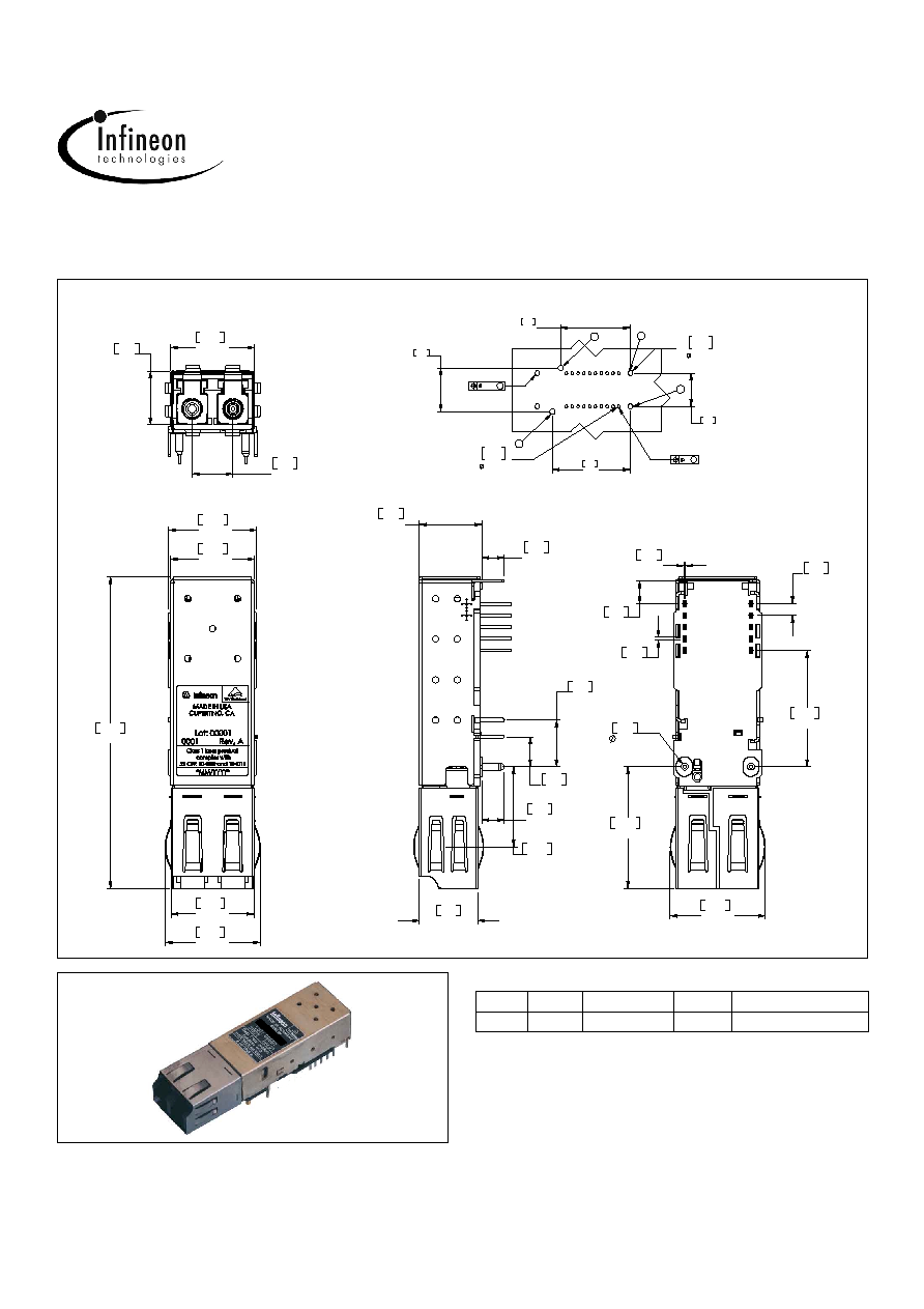
Circuit Board Layout
Recommended PCB Thickness: 0.1(2.54) max.
1.78
.070
3.48
.137
17.78
.700
20X
0.81
0
0
.03
-.00
+.00
6X
1.40
0
0
.06
-.00
+.00
21.34
.840
13.34
.525
10.16
.400
23.88
.940
(10X)
1
1
1
1
1. 4 optional package grounding tabs
10 pin module requires only 12 PCB holes.
0.05M
0 M
V23818-K305-L56
Dimensions in [mm] inches
V
2
3
8
1
8
-K
3
0
5
-L
5
6
Input
Output
Signal detect
Voltage
Part number
AC
AC
TTL
3.3 V
V23818-K305-L56

Fiber Optics
V23818-K305-L56, SFF, MM 850nm 1.0625 GBd Fibre Channel, 1.3 GBE 2x5 Trx (LCTM), ext.temp.
2
FEATURES
∑ Small Form Factor transceiver
∑ RJ-45 style LCTM connector system
∑ Half the size of SC Duplex 1x9 transceiver
∑ Single power supply (3.3 V)
∑ Extremely low power consumption
∑ PECL and LVPECL differential inputs and outputs
∑ System optimized for 62.5/50
µ
m graded index fiber
∑ Multisource footprint
∑ Small footprint for high channel density
∑ UL-94 V-0 certified
∑ ESD Class 1 per MIL-STD 883D Method 3015.7
∑ Compliant with FCC (Class B) and EN 55022
∑ For distances of up to 550 m
∑ Class 1 FDA and IEC laser safety compliant
∑ Extended Temperature Range ≠40∞C to 85∞C
Absolute Maximum Ratings
Exceeding any one of these values may destroy the device
immediately.
Package Power Dissipation................................................ 1.5 W
Data Input Levels (PECL) ............................................V
CC
+0.5 V
Differential Data Input Voltage .............................................1.6 V
Operating Case Temperature...............................≠40 ∞ C to 85∞ C
Storage Ambient Temperature............................. ≠40 ∞ C to 85∞C
Soldering Conditions, Temp/Time
(MIL-STD 883C, Method 2003) ........................... 250 ∞C/ 5.5 s
V
CC
max.............................................................................. 5.5 V
ECL-Output current data ...................................................50 mA
DESCRIPTION
The Infineon Gigabit Ethernet multimode transceiver ≠ part of
Infineon Small Form Factor transceiver family ≠ is based on the
Physical Medium Depend (PMD) sublayer and baseband
medium, type 1000BASE-SX (short wavelength), Fibre Channel
DC 100-M5-SN-I and 100-M6-SN-I.
The appropriate fiber optic cable is 62.5 µm or 50 µm multi-
mode fiber with LCTM connector.
Operating range for over each optical fiber type
The Infineon Gigabit Ethernet multimode transceiver is a single
unit comprised of a transmitter, a receiver, and an LCTM recepta-
cle. This design frees the customer from many alignment and
PC board layout concerns.
This transceiver supports the LCTM connectorization concept. It
is compatible with RJ-45 style backpanels for high end
Data Com and Telecom applications while providing the advan-
tages of fiber optic technology.
The module is designed for low cost SAN, LAN, WAN, Fibre
Channel and Gigabit Ethernet applications. It can be used as the
network end device interface in mainframes, workstations,
servers, and storage devices, and in a broad range of network
devices such as bridges, routers, hubs, and local and wide area
switches.
This transceiver operates at 1 and 1.25 Gbit/s from a single
power supply (+3.3 V). The full differential data inputs and out-
puts are PECL and LVPECL compatible.
Functional Description of 2x5 Pin Row Transceiver
This transceiver is designed to transmit serial data via
multimode cable.
Functional Diagram
The receiver component converts the optical serial data into
PECL compatible electrical data (RD and RDnot). The Signal
Detect (SD, active high) shows whether an optical signal is
present.
The transmitter converts PECL compatible electrical serial data
(TD and TDnot) into optical serial data. Data lines are differen-
tially 100
terminated.
The transmitter contains a laser driver circuit that drives the
modulation and bias current of the laser diode. The currents are
controlled by a power control circuit to guarantee constant out-
put power of the laser over temperature and aging.
The power control uses the output of the monitor PIN diode
(mechanically built into the laser coupling unit) as a controlling
signal, to prevent the laser power from exceeding the operating
limits.
Single fault condition is ensured by means of an integrated
automatic shutdown circuit that disables the laser when it
detects laser fault to guarantee the laser Eye Safety.
The transceiver contains a supervisory circuit to control the
power supply. This circuit makes an internal reset signal when-
ever the supply voltage drops below the reset threshold. It
keeps the reset signal active for at least 140 milliseconds after
the voltage has risen above the reset threshold. During this
time the laser is inactive.
The laser can be disabled by the TxDis input.
Fiber type
Minimum range (meters)
Typ.
62.5 micron MFF
2 to 260
400
50.0 micron MFF
2 to 550
700
10 micron SFF
Not supported
Laser
Driver
Power
Control
Receiver
o/e
o/e
Laser
e/o
Rx Coupling Unit
TD
-
TD+
TxDis
RD
-
RD+
SD
Laser
Coupling Unit
Multimode Fiber
LEN
Monitor
Automatic
Shut-Down

Fiber Optics
V23818-K305-L56, SFF, MM 850nm 1.0625 GBd Fibre Channel, 1.3 GBE 2x5 Trx (LCTM), ext.temp.
3
TECHNICAL DATA
The electro-optical characteristics described in the following
tables are valid only for use under the recommended operating
conditions.
Recommended Operating Conditions
Transmitter Electro-Optical Characteristics
Notes
1. Into multimode fiber, 62.5 µm or 50 µm diameter.
2. Laser power is shut down if power supply is below VTH and
switched on if power supply is above VTH after tRES.
Receiver Electro-Optical Characteristics
Notes
1. Average optical power at which the BER is 1 x 10E≠12. Measured
with a 2
7
≠1 NRZ PRBS and ER=9 dB.
2. An increase in optical power above the specified level will cause the
SIGNAL DETECT output to switch from a Low state to a High state.
3. A decrease in optical power below the specified level will cause the
SIGNAL DETECT to change from a High state to a Low state.
4. AC/AC for data. Load 50
to GND or 100
differential. For dynamic
measurement a tolerance of 50 mV should be added.
5. Supply current excluding Rx output load.
Parameter
Symbol
Min.
Typ.
Max.
Units
Case Temperature
T
C
≠40
85
∞
C
Power Supply Voltage
V
CC
≠V
EE
3.1
3.3
3.5
V
Transmitter
Data Input
Differential Voltage
V
DIFF
250
1600
mV
Receiver
Input Center
Wavelength
C
770
860
nm
Transmitter Symbol Min. Typ. Max. Units
Launched Power
(Average)
(1)
P
O
≠9.5
≠4
dBm
Center Wavelength
C
830
850
860
nm
Spectral Width (RMS)
l
0.85
Relative Intensity Noise
RIN
≠117
dB/Hz
Extinction Ratio (Dynamic)
ER
8
dB
Reset Threshold
(2)
V
TH
2.2
2.7
2.99
V
Reset Time Out
(2)
t
RES
140
240
560
ms
Rise Time, 20%≠80%
t
R
0.26
ns
Supply Current
75
mA
Receiver
Symbol Min.
Typ.
Max.
Units
Sensitivity
(Average Power)
(1)
P
IN
≠19
≠16.5
dBm
Saturation
(Average Power)
P
SAT
0
Signal Detect
Assert Level
(2)
P
SDA
≠24
≠18
Signal Detect
Deassert Level
(3)
P
SDD
≠30
≠27
Signal Detect
Hysteresis
P
SDA
≠
P
SDD
3
dB
Signal Detect
Assert Time
t
ASS
100
µ
s
Signal Detect
Deassert Time
t
DAS
350
Data Output
Differential Voltage
(4)
V
DIFF
0.5
0.8
1.23
V
Return Loss
of Receiver
A
RL
12
dB
Supply current
(5)
60
mA

Fiber Optics
V23818-K305-L56, SFF, MM 850nm 1.0625 GBd Fibre Channel, 1.3 GBE 2x5 Trx (LCTM), ext.temp.
4
Pin Description
Regulatory Compliance
EYE SAFETY
This laser based multimode transceiver is a Class 1 product. It
complies with IEC 60825-1 and FDA 21 CFR 1040.10 and
1040.11.
To meet laser safety requirements the transceiver shall be oper-
ated within the maximum operating limits.
Caution
All adjustments have been made at the factory prior to ship-
ment of the devices. No maintenance or alteration to the
device is required.
Tampering with or modifying the performance of the device
will result in voided product warranty.
Note
Failure to adhere to the above restrictions could result in a modifica-
tion that is considered an act of "manufacturing", and will require,
under law, recertification of the modified product with the U.S. Food
and Drug Administration (ref. 21 CFR 1040.10 (i)).
Laser Data
Required Labels
Laser Emission
Pin Name
Level/
Logic
Pin# Description
V
EEr
Receiver
Signal Ground
N/A
1
V
CCr
Receiver
Power Supply
N/A
2
SD
Signal Detect
TTL
3
Normal Operation: Logic
"1" Output, represents
that light is present at re-
ceiver input
Fault Condition: Logic "0"
Output
RD≠
Received Data
Out Not
PECL
4
RD+
Received Data
Out
PECL
5
V
CCt
N/A
6
Transmitter Power Supply
V
EEt
N/A
7
Transmitter Signal Ground
TxDis Transmitter
Disable/Enable
TTL-
Input
8
A low signal switches the
laser on.
A high signal switches the
laser off.
TD+
Transmit Data
PECL
9
Transmitter Data In
TD≠
Transmit Data
Not
PECL
10
Transmitter Data In
MS
MS
Package
Grounding
Tabs
N/A
MS1
MS2
T1
T2
T3
T4
Mounting Studs and
grounding Tabs are provid-
ed for transceiver mechan-
ical attachment to the
circuit board. They also
provide an optional connec-
tion of the transceiver to
the equipment chassis
ground.
The holes in the circuit
board must be tied to
chassis ground.
Feature
Standard
Comments
Electrostatic Discharge
(ESD) to the Electrical
Pins
MIL-STD 883D
Method 3015.7
Class 1 (>1000 V)
Immunity:
Electrostatic Discharge
(ESD) to the Duplex SC
Receptacle
EN 61000-4-2
IEC 61000-4-2
Discharges of
±
15 kV
with an air discharge
probe on the recepta-
cle cause no damage.
Immunity:
Radio Frequency
Electromagnetic Field
EN 61000-4-3
IEC 61000-4-3
With a field strength
of 3 V/m rms, noise
frequency ranges
from 10 MHz to
1 GHz. No effect on
transceiver perfor-
mance between the
specification limits.
Emission:
Electromagnetic
Interference (EMI)
FCC Class B
EN 55022
Class B CISPR 22
Noise frequency
range:
30 MHz to 6 GHz
Wavelength
850 nm
Total output power (as defined by IEC: 7 mm
aperture at 1.4 cm distance)
<675 µW
Total output power (as defined by FDA: 7 mm
aperture at 20 cm distance)
<70 µW
Beam divergence
12
∞
Class 1 Laser Product
IEC
Complies with 21 CFR
1040.10 and 1040.11
FDA
10 9 8 7 6
1 2 3 4 5
Tx
Rx
Indication of
laser aperture
and beam

Fiber Optics
V23818-K305-L56, SFF, MM 850nm 1.0625 GBd Fibre Channel, 1.3 GBE 2x5 Trx (LCTM), ext.temp.
5
APPLICATION NOTES
EMI-Recommendation
To avoid electromagnetic radiation exceeding the required limits
please read the following recommendations:
Whenever high speed Gigabit switching components are
located on the PCB (also multiplexers, clock recoveries ...) any
opening of the machine may generate radiation even at differ-
ent locations. Thus every mechanical opening or aperture
should be as small as possible.
On the board itself every data connection should be an imped-
ance matched line (e.g. strip line, coplanar strip line). Data,
Datanot should be routed symmetrically, via's should be
avoided. A symmetrically matching resistor of 100
should be
placed at the end of each matched line. An alternative termina-
tion can be provided with a 50
resistor at each (D, Dn). In DC
coupled systems an artificial 50
resistance can be achieved
as follows: For 3.3 V: 125
to V
CC
and 82
to V
EE
, for 5 V:
82
to V
CC
and 125
to V
EE
at Data and Datanot. Please con-
sider whether there is an internal termination inside an IC or a
transceiver.
It is recommended that chassis GND and signal GND should
remain separate if there are openings or apertures of the hous-
ing nearby. Sometimes signal GND is the most harmful source
of radiation. Connecting chassis GND and signal GND at the
plate/ bezel/ backside wall e.g. by means of a fiber optic trans-
ceiver may result in a huge amount of radiation. Even a capaci-
tive coupling between signal GND and chassis may be harmful
if it is to close to an opening or an aperture.
If a separation of signal GND and chassis GND is not possible,
it is strongly recommended to provide a proper contact
between signal GND and chassis GND at almost every location.
This concept is suitable to avoid hotspots. Hotspots are places
of highest radiation which could be generated if only a few con-
nections between signal and chassis GND are available. Com-
pensation currents would concentrate at these connections,
causing radiation.
For the SFF transceiver a connection of the 4 housing pins to
chassis GND is recommended. If no separate chassis GND is
available on the users PCB the pins should be connected to sig-
nal GND. In this case take care of the notes above.
Please consider that the PCB may behave like a waveguide.
With an
r
of 4, the wavelength of the harmonics inside the
PCB will be half of that in free space. In this case even small
PCBs may have unexpected resonances.
Multimode 850 nm Gigabit Ethernet/Fibre Channel 2x5 Transceiver, AC/AC
Values of R1/2/3/4 may vary as long as proper 50
termination
to V
EE
or 100
differential is provided. The power supply filter-
ing is required for good EMI performance. Use short tracks
from the inductor L1/L2 to the module V
CC
Rx/V
CC
Tx.
The transceiver contains an automatic shutdown circuit. Reset
is only possible if the power is turned off, and then on again.
(V
CC
Tx switched below V
TH
).
Application Board available on request.
VCSEL
Driver
Signal
Detect
Limiting
Amplifier
Pre-
Amp
RD-
RD+
Tx+
Tx-
Serializer/
Deserializer
Gigabit
Transceiver
Chip
ECL/PECL
Driver
Receiver
PLL etc.
Infineon Transceiver
V23818-K305-L56
1
5
4
3
2
6
10
9
7
SD to upper level
V
EEt
TD+
TD-
V
CCt
V
CCr
SD
RD-
RD+
V
EEr
V
CC
R7
R8
L1
L2
C2
C1
R3
R4
R1
R2
C3
V
CC
SerDes
3.3 V
V
CC
3.3 V
100
TTL level
8
TxDis
C1/2/3 = 4.7
µ
F
L1/2
= 1
µ
H
R1/2
= Depends on SerDes chip used
R3/4
= Depends on SerDes chip used
R7/8 = Biasing (depends on SerDes chip)
Place R1/2/3/4/7/8 close to SerDes chip
Place R5/6 close to Infineon transceiver