Data Sheet
1
2003-09-10
Part Number
Voltage
Signal
Detect
Operating
Temperature
Input
Output
V23818-N15-L616
3.3 V
LVPECL
≠40...80∞C
DC
DC
V23818-N15-L653
3.3 V
LVTTL
0...70∞C
AC
AC
V23818-N15-L656
≠40...80∞C
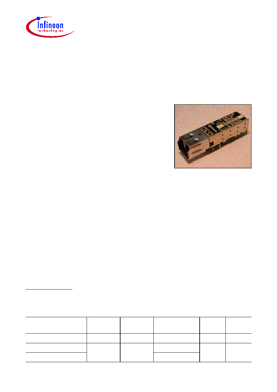
Small Form Factor
Single Mode 1300 nm
Multirate up to 2.5 Gbit/s Transceiver
2x10 Pinning with LCTM Connector, with Collar
File: 1119
Fiber Optics
LCTM is a trademark of Lucent
V23818-N15-L6xx
Features
∑ Small Form Factor transceiver
∑ Multisource 2x10 footprint, SFF MSA compliant
1)
∑ Small footprint for high port density
∑ RJ-45 style LCTM connector system
∑ Half the size of SC Duplex 1x9 transceiver
∑ Compliant with SDH STM-16 / SONET OC-48
standards
∑ Suitable for multirate applications up to 2.5 Gbit/s
∑ Single power supply (3.3 V)
∑ Extremely low power consumption, 600 mW typical
∑ Loss of optical signal indicator
∑ Tx and Rx power monitor functions
∑ Laser disable, LVTTL input
∑ LVPECL differential inputs and outputs
∑ For distance of up to 15 km on single mode fiber (SMF)
∑ Class 1 FDA and IEC laser safety compliant
∑ UL 94 V-0 certified
∑ Compliant with FCC (Class B) and EN 55022
1)
Current MSA documentation can be found at www.infineon.com/fiberoptics

V23818-N15-L6xx
Pin Configuration
Data Sheet
2
2003-09-10
Pin Configuration
Figure 1
Pin Connect Diagram
Pin Description
Pin
No.
Symbol
Level/Logic
Description
1
PDBias
DC current
PIN photo detector bias current
2
V
EEr
Ground
Receiver signal ground
3
V
EEr
Ground
Receiver signal ground
4
NC
Not connected
5
NC
Not connected
6
V
EEr
Ground
Receiver signal ground
7
V
CCr
Power supply
Receiver power supply
8
SD
LVTTL or LVPECL output
1)
1)
LVPECL output active high for V23818-N15-L616.
LVTTL output active high for V23818-N15-L653/L656.
Receiver optical input level monitor
9
RD≠
LVPECL output
Receiver data out bar
10
RD+
LVPECL output
Receiver data out
11
V
CCt
Power supply
Transmitter power supply
12
V
EEt
Ground
Transmitter signal ground
13
TDis
LVTTL input
Transmitter disable
14
TD+
LVPECL input
Transmitter data in
15
TD≠
LVPECL input
Transmitter data in bar
16
V
EEt
Ground
Transmitter signal ground
17
BMon≠
DC voltage
Laser diode bias current monitor
18
BMon+
DC voltage
Laser diode bias current monitor
19
PMon≠
DC voltage
Laser diode optical power monitor
20
PMon+
DC voltage
Laser diode optical power monitor
MS
Mounting studs
HL
Housing leads
Tx
Rx
HL
HL
HL
HL
6 7 8 9 10
11
12
13
14
15
1 2 3 4 5
16
17
18
19
20
TOP VIEW
MS
MS
File: 1335

V23818-N15-L6xx
Pin Configuration
Data Sheet
3
2003-09-10
V
EEr
/
V
EEt
Connect pins 2, 3, 6, 12 and 16 to signal ground.
V
CCr
/
V
CCt
A 3.3 V
DC power supply must be applied at pins 7 and 11. A recommended power
supply filter network is given in the termination scheme. Locate power supply filtering
directly at the transceiver power supply pins. Proper power supply filtering is essential
for good EMI performance.
TD+ / TD≠
Transmitter data LVPECL level inputs. For V23818-N15-L653/L656 terminated and AC
coupled internally. For V23818-N15-L616 use termination and coupling as shown in the
termination scheme.
RD≠ / RD+
Receiver data LVPECL level outputs. For V23818-N15-L653/L656 biased and AC
coupled internally. For V23818-N15-L616 use termination and coupling as shown in the
termination scheme.
TDis
A logical LVTTL high input will disable the laser. To enable the laser, an LVTTL low input
must be applied. Leave pin unconnected if feature not required.
SD
LVTTL output for V23818-N15-L653/L656. LVPECL output for V23818-N15-L616.
A logical high output indicates normal optical input levels to the receiver. Low optical
input levels at the receiver result in an LVTTL low output. Signal Detect can be used to
determine a definite optical link failure; break in fiber, unplugging of a connector, faulty
laser source. However it is not a detection of a bad link due to data-related errors.
MS
Mounting studs are provided for transceiver mechanical attachment to the circuit board.
They also provide an optional connection of the transceiver to the equipment chassis
ground. The holes in the circuit board must be tied to chassis ground.
HL
Housing leads are provided for additional signal grounding. The holes in the circuit board
must be included and tied to signal ground.

V23818-N15-L6xx
Pin Configuration
Data Sheet
4
2003-09-10
PDBias
Connect pin 1 to
V
CC
through a bias resistor, of a value not exceeding 2 k
, as shown in
Figure 2
to monitor PIN photo detector bias current. Leave pin floating if not used.
Typical behaviour is shown in
Figure 3
and
Figure 4
using a 2 k
load.
Figure 2
Photo Detector Bias Interface
2 k
V
CC
Pin 1
V
bias
File: 1307

V23818-N15-L6xx
Pin Configuration
Data Sheet
5
2003-09-10
Typical Responsitivity of PIN Photo Detector Bias Current Monitor
Figure 3
Linear Response
Figure 4
Logarithmic Response
0
100
200
300
400
0
100
200
300
400
Received Optical Power (
µ
W)
Photo Detector Monitor Current (
µ
A)
File: 1308
0
100
200
300
400
-
30
-
24
-
18
-
12
-
6
0
Received Optical Power (dBm)
Photo Detector Monitor Current (
µ
A)
File: 1309