Fiber Optics
JANUARY 2000
V23826-H18-C
(*)
Single Mode 622 MBd ATM/SDH/SONET 1x9 Transceiver
FEATURES
∑ Compliant with ATM, SONET OC-3, SDH STM-1 and
SONET OC-12, SDH STM-4
∑ Meets mezzanine standard height of 9.8 mm
∑ Compact integrated transceiver unit with
≠ MQW laser diode transmitter
≠ InGaAs PIN photodiode receiver
≠ Duplex SC receptacle
∑ Class 1 FDA and IEC laser safety compliant
∑ FDA Accession No. 9520890-12, 9520890-13
∑ Single power supply (5 V or 3.3 V)
∑ Signal detect indicator (PECL and TTL versions)
∑ PECL differential inputs and outputs
∑ Process plug included
∑ Input Signal Monitor (DC/DC Version)
∑ Wave solderable and washable with process plug
inserted
∑ Industry standard multisource 1x9 footprint
∑ For distances of up to 15 km on single mode fiber
Absolute Maximum Ratings
Exceeding any one of these values may destroy the device
immediately.
Package Power Dissipation
(1) ........................................................
1.5 W
Supply Voltage (V
CC
≠V
EE
) 5 V............................................. 7 V
3.3 V.......................................... 5 V
Data Input Levels........................................................V
CC
+0.5 V
Differential Data Input Voltage ............................................ 2.5 V
Operating Ambient Temperature .............................0 ∞C to 70 ∞C
Storage Ambient Temperature ............................ ≠40 ∞C to 85∞C
Soldering Conditions Temp/Time
(MIL-STD 883C, Method 2003) ............................. 250 ∞C/5.5s
Note
1. For
V
CC
≠V
EE
(min., max.). 50% duty cycle. The supply current does
not include the load drive current of the receiver output.
*) Ordering Information
Note
1. Standard
version
(8.6 max)
.343 max
4.875
.1
9
2
(0.35
≠
0.
1)
.0
1
4
≠
.0
04
(3.8 max)
.15 max
2
(2.8 max)
.
1
1 max
0.3
.012
M
A
A
M
(1
.4 -0.05)
.0
05 -.0
02
2x
4
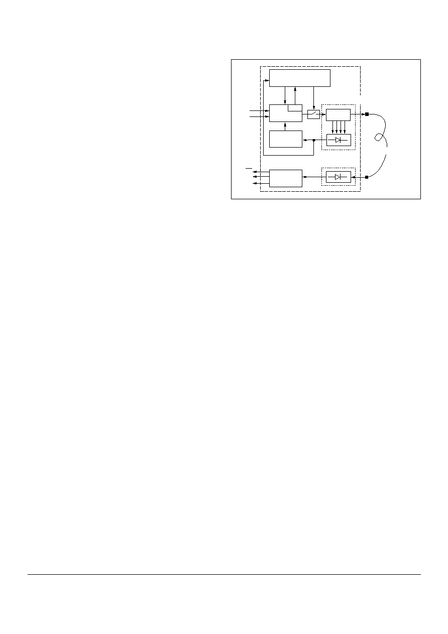
product label
1
(9.79 max)
.385 max
2
.08
(0.6
≠
0.
1)
.024
≠
.0
04
(3.3
≠
0.2)
.1
3
0
≠
.0
08
(1≠0.1)
.04≠.004
(0.63
≠
0.2)
.025
≠
.0
08
(
0.46
≠
0.05)
.0
1
8
≠
.0
02
9x
0.3
.0
1
2
M
A
A
0.1
.004
M
M
PC boar
d
(25.25
≠
0.05)
.994
≠
.0
02
A
2.54
.1
20.32
.8
8x
8x
123
4
5
6
7
8
9
Z
(2.05
≠
0.05)
.079
≠
.0
02
12
.
7
.5
(2.5≠0.1)
.098≠.002
DUPLEX
SC
RECEPT
A
CLE
5
1
32
3
(11 max)
.433 max
(15.88≠0.5)
.625≠.02
(38.6≠0.15)
1.52≠.006
20.32
.8
M
OPTICAL
CENTERLINE
(PC boar
d
thic
kness)
Vi
ew
Z
(lead cr
oss section
and st
andof
f siz
e)
11x
M
M
0.
1
.0
04
9x
(0.8
≠
0.
1)
.032
≠
.0
04
2.54
20.32
.1
.
8
8x
8x
(2.54)
.1
(2.54)
.1
20.32
.8
(1
.9
≠
0.
1)
.075
≠
.0
04
11
x
2x
(Footprint)
TRX without shield
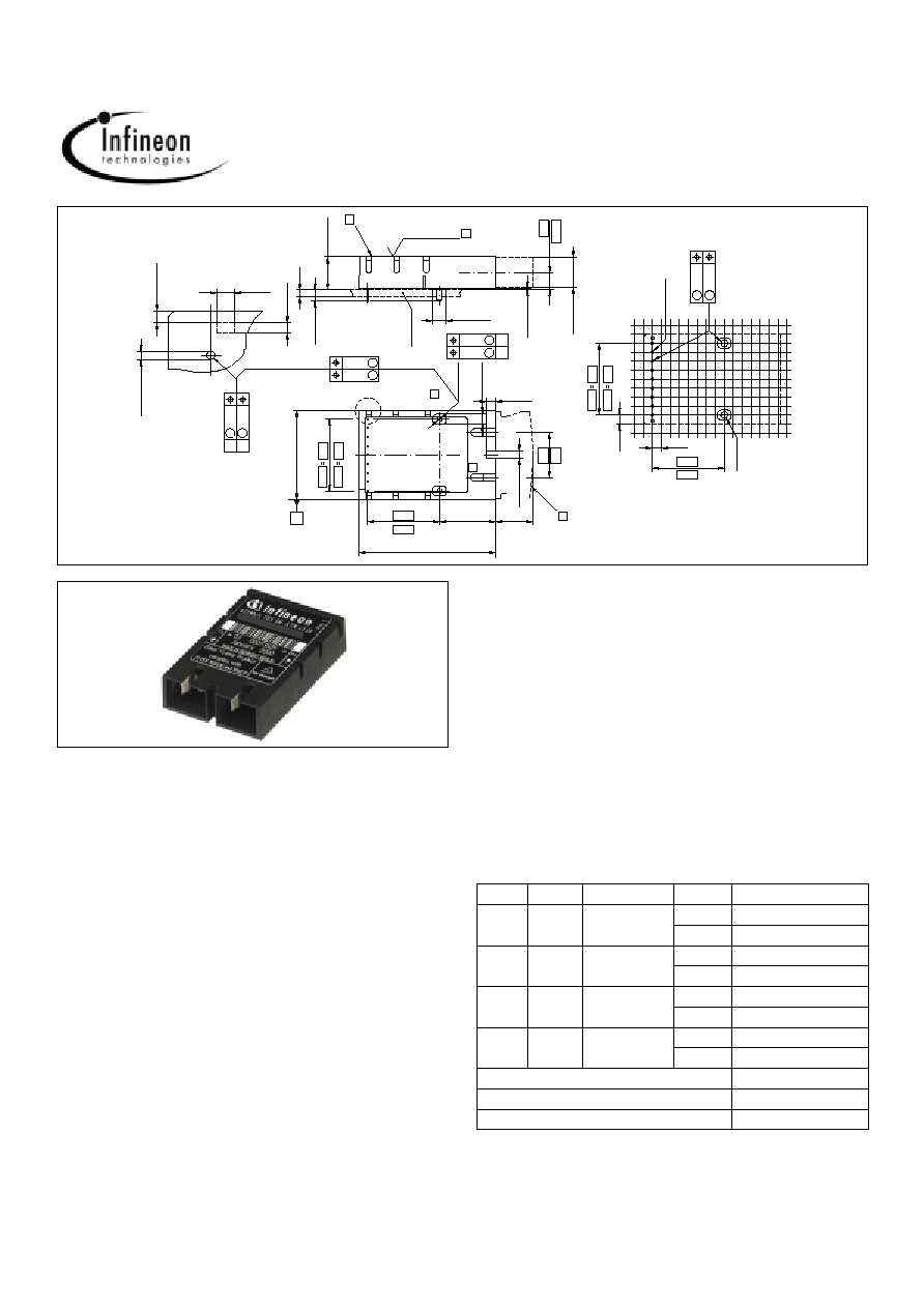
Dimensions in (mm) inches
V23826-H1
8-C363
Input
Output
Signal detect
Voltage
Part number
AC
DC
PECL
5 V
V23826-H18-C13
3.3 V
V23826-H18-C313
AC
AC
TTL
5 V
V23826-H18-C53
3.3 V
V23826-H18-C353
DC
DC
PECL
5 V
V23826-H18-C63
(1)
3.3 V
V23826-H18-C363
(1)
AC
AC
PECL
5 V
V23826-H18-C73
3.3 V
V23826-H18-C373
Shield options
Add suffix to PIN
Metallized cover, forward springs
-C3
Metallized cover, backward springs
-D3
Fiber Optics
V23826-H18-C13/C53/C63/C73, SM 622 MBd ATM/SDH/SONET 1x9 Trx
2
DESCRIPTION
The Infineon single mode ATM transceiver complies with the
ATM Forum's Network Compatible ATM for Local Network
Applications document and ANSI's Broadband ISDN--Cus-
tomer Installation Interfaces, Physical Media Dependent Speci-
fication, T1.646-1995, Bellcore - SONET OC-3 / IR-1 and OC-12 /
IR-1, ITU-T G.957 STM-1 / S.1.1 and STM-4 / S.4.1. ATM was
developed to facilitate solutions in multimedia applications and
real time transmission. The data rate is scalable, and the ATM
protocol is the basis of the broadband public networks being
standardized in the International Telecommunications Union
(ITU), the former International Telegraph and Telephone Consul-
tative Committee (CCITT). ATM can also be used in local private
applications.
The Infineon single mode ATM transceiver is a single unit com-
prised of a transmitter, a receiver, and an SC receptacle. This
design frees the customer from many alignment and PC board
layout concerns. The module is designed for low cost WAN
applications. It can be used as the network end device interface
in workstations, servers, and storage devices, and in a broad
range of network devices such as bridges, routers, and intelli-
gent hubs, as well as wide area ATM switches.
This transceiver operates at 622.080 Mbit/s from a single
power supply (+5 Volt or 3.3 Volt). The differential data inputs
and outputs are PECL compatible.
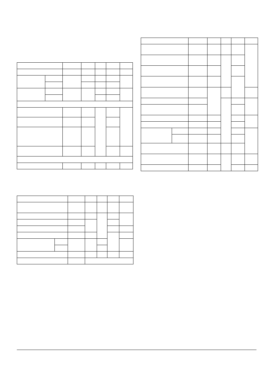
Functional Description
This transceiver is designed to transmit serial data via single
mode cable.
Functional Diagram
The receiver component converts the optical serial data into
PECL compatible electrical data (RD and RDnot). The Signal
Detect (SD, active high) shows whether optical data is
present
(1)
.
The transmitter converts electrical PECL compatible serial data
(TD and TDnot) into optical serial data.
The following versions are available:
1. AC/DC Transceiver
Tx is AC coupled with differential 100
load. Rx has standard
PECL output and is DC coupled.
2. AC/AC TTL Transceiver
Tx and Rx are AC coupled. Tx has differential 100
load. Signal
Detect is TTL compatible.
3. DC/DC Transceiver
Standard PECL inputs and outputs Tx and Rx are DC coupled.
This version contains an Input Signal Monitor (ISM), that
switches off the optical power if a continuously low level is
applied at Data Input.
4. AC/AC PECL Transceiver
Tx and Rx are AC coupled. Tx has differential 100
load. Signal
Detect is PECL compatible.
The transmitter contains a laser driver circuit that drives the
modulation and bias current of the laser diode. The currents are
controlled by a power control circuit to guarantee constant out-
put power of the laser over temperature and aging.
The power control uses the output of the monitor PIN diode
(mechanically built into the laser coupling unit) as a controlling
signal, to prevent the laser power from exceeding the operating
limits.
Single fault condition is ensured by means of an integrated
automatic shutdown circuit that disables the laser when it
detects transmitter failures. A reset is only possible by turning
the power off, and then on again.
The transceiver contains a supervisory circuit to control the
power supply. This circuit generates an internal reset signal
whenever the supply voltage drops below the reset threshold.
It keeps the reset signal active for at least 15 milliseconds after
the voltage has risen above the reset threshold. During this
time the laser is inactive.
Note
1. We recommend to switch off the transmitter supply (V
CC
-Tx) if no
transmitter input data is applied.
Laser
Driver
Power
Control
Receiver
o/e
o/e
Laser
e/o
RX Coupling Unit
TD
TD
RD
RD
SD
Laser Coupling Unit
Single Mode Fiber
LEN
Monitor
Signal Monitor and
Automatic Shut-Down
ISM*
*DC/DC Version only
Fiber Optics
V23826-H18-C13/C53/C63/C73, SM 622 MBd ATM/SDH/SONET 1x9 Trx
3
TECHNICAL DATA
The electro-optical characteristics described in the following
tables are only valid for use under the recommended operating
conditions.
Recommended Operating Conditions
Note
1. For
V
CC
≠V
EE
(min., max.) 50% duty cycle. The supply current does
not include the load drive current of the receiver output.
Transmitter Electro-Optical Characteristics
Notes
1. Into single mode fiber, 9 µm diameter.
2. Laser power is shut down if power supply is below V
TH
and
switched on if power supply is above V
TH
after t
RES
.
3. Transmitter meets ANSI T1E1.2, SONET OC-3 and OC-12, and
ITU-T G.957 mask patterns.
Receiver Electro-Optical Characteristics
Notes
1. Minimum average optical power at which the BER is less than
1x10
-12
or lower. Measured with a 2
23
-1 NRZ PRBS as recom-
mended by ANSI T1E1.2, SONET OC-3 and OC-12, and ITU-T G.957.
2. An increase in optical power above the specified level will cause the
SIGNAL DETECT output to switch from a Low state to a High state.
3. A decrease in optical power below the specified level will cause the
SIGNAL DETECT to change from a High state to a Low state.
4.
DC/DC, AC/DC for data
DC/DC, AC/DC, AC/AC PECL for Signal Detect
PECL compatible. Load is 50
into V
CC
≠2 V for data, 510
(5 V) or
270
(3.3 V) to V
((
for Signal Detect. Measured under DC condi-
tions. For dynamic measurements a tolerance of 50 mV should be
added. V
CC
=3.3 V/5 V. T
AMB
=25∞C.
5. Max. output current high:
≠
0.4 mA (drive current)
low: +2.0 mA (sink current)
6. AC/AC for data. Load 50
to GND or 100
differential. For dynamic
measurement a tolerance of 50mV should be added.
Parameter
Symbol
Min.
Typ. Max.
Units
Ambient Temperature
T
AMB
0
70
∞C
Power Supply
Voltage
3.3 V
V
CC
≠V
EE
3.1
3.3
3.5
V
5 V
4.75
5
5.25
Supply
Current
(1)
3.3 V
I
CC
160
230
mA
5 V
180
270
Transmitter
Data Input High Voltage
DC/DC
V
IH
≠V
CC
≠1165
≠880
mV
Data Input Low Voltage
DC/DC
V
IL
≠V
CC
≠1810
≠1475
Data Input Differential
Voltage
AC/DC, AC/AC TTL,
AC/AC PECL
V
DIFF
250
1600
Input Data Rise/Fall
Time 10%≠90%
t
R
, t
F
100
1300
ps
Receiver
Input Center Wavelength
C
1270
1356
nm
Transmitter
Symbol Min. Typ. Max. Units
Launched Power
(Average)
(1)
P
O
≠15
≠11
≠8
dBm
Center Wavelength
C
1274
1356 nm
Spectral Width (RMS)
l
2.5
Relative Intensity Noise
RIN
≠120
dB/Hz
Extinction Ratio (Dynamic)
ER
8.2
dB
Reset Threshold
(2)
3.3 V
V
TH
2.7
V
5 V
3.5
Reset Time Out
(2)
t
RES
15
22
35
ms
Eye Diagram
(3)
ED
Receiver
Symbol
Min.
Typ. Max.
Units
Sensitivity
(Average Power)
(1)
P
IN
≠30
≠28
dBm
Saturation
(Average Power)
P
SAT
≠8
Signal Detect
Assert Level
(2)
P
SDA
≠28
Signal Detect
Deassert Level
(3)
P
SDD
≠38
Signal Detect Hysteresis
P
SDA
≠
P
SDD
1.5
dB
Signal Detect Assert Time t
ASS
100
µ
s
Signal Detect Deassert
Time
t
DAS
350
Output Low Voltage
(4)
V
OL
-V
CC
≠1950
≠1620 mV
Output High Voltage
(4)
V
OH
-V
CC
≠1025
≠720
Signal Detect
Output Voltage
AC/AC TTL
(5)
Low
V
SDL
0.5
V
High
V
SDH
2
Data Output Differential
Voltage
(6)
V
DIFF
0.5
0.8
1.23
Output Data Rise/Fall
Time, 20%≠80%
t
R
, t
F
375
ps
Return Loss of Receiver
A
RL
12
dB
Fiber Optics
V23826-H18-C13/C53/C63/C73, SM 622 MBd ATM/SDH/SONET 1x9 Trx
4
Pin Description
Regulatory Compliance
EYE SAFETY
This laser based single mode transceiver is a Class 1 product. It
complies with IEC 60825-1 and FDA 21 CFR 1040.10 and
1040.11.
To meet laser safety requirements the transceiver shall be oper-
ated within the Absolute Maximum Ratings.
Caution
All adjustments have been made at the factory prior to ship-
ment of the devices. No maintenance or alteration to the
device is required.
Tampering with or modifying the performance of the device
will result in voided product warranty.
Note
Failure to adhere to the above restrictions could result in a modifica-
tion that is considered an act of "manufacturing," and will require,
under law, recertification of the modified product with the U.S. Food
and Drug Administration (ref. 21 CFR 1040.10 (i)).
Laser Data
Required Labels
Laser Emission
APPLICATION NOTE
ATM transceivers and matching circuits are high frequency
components and shall be terminated as recommended in the
application notes for proper EMI performance. Electromagnetic
emission may be caused by these components.
To prevent emissions it is recommended that cutouts for the
fiber connectors be designed as small as possible.
It is recommended that the Tx plug and the Rx plug be
separated with a bar that divides the duplex SC opening.
Pin Name
Level / Logic
Pin# Description
RxV
EE
Rx Ground
Power Supply
1
Negative power
supply, normally
ground
RD
Rx Output
Data
PECL Output
2
Receiver output
data
RDn
3
Inverted receiver
output data
SD
Rx Signal
Detect
PECL or TTL
4
A high level on this
output shows that
optical data is ap-
plied to the optical
input.
RxV
CC
Rx 3.3 V/5 V Power Supply
5
Positive power sup-
ply, 3.3 V/5 V
TxV
CC
Tx 3.3 V/5 V
6
TDn Tx
Input
Data
PECL Input
7
Inverted transmitter
input data
TD
8
Transmitter input
data
TxV
EE
Tx Ground
Power Supply
9
Negative power
supply, normally
ground
Stud Pin
Mech. Support S1/2
Not connected
Feature
Standard
Comments
Electrostatic
Discharge (ESD)
to the Electrical
Pins
MIL-STD 883C
Method 3015.7
Class 1 (>1000 V)
Immunity:
Electrostatic
Discharge (ESD)
to the Duplex SC
Receptacle
EN 61000-4-2
IEC 61000-4-2
Discharges of ±15kV with
an air discharge probe on
the receptacle cause no
damage.
Immunity:
Radio Frequency
Electromagnetic
Field
EN 61000-4-3
IEC 61000-4-3
With a field strength of
3 V/m rms, noise
frequency ranges from
10 MHz to 1 GHz. No
effect on transceiver per-
formance between the
specification limits.
Emission:
Electromagnetic
Interference EMI
FCC Class B
EN 55022 Class B
CISPR 22
Noise frequency range:
30 MHz to 6 GHz; Margins
depend on PCB layout and
chassis design
Wavelength
1300 nm
Total output power (as defined by IEC: 50 mm
aperture at 10 cm distance)
less than
2 mW
Total output power (as defined by FDA: 7 mm
aperture at 20 cm distance)
less than
180 µW
Beam divergence
4∞
Class 1 Laser Product
IEC
Complies with 21 CFR
1040.10 and 1040.11
FDA
Indication of laser
aperture and beam
Fiber Optics
V23826-H18-C13/C53/C63/C73, SM 622 MBd ATM/SDH/SONET 1x9 Trx
5
APPLICATION NOTE
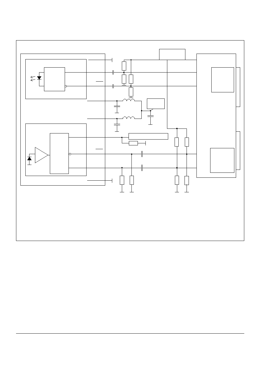
Single Mode 622 MBd ATM 1x9 Transceiver, DC/DC Version
The following Application Notes assume Fiber Optic
Transceivers using 5 V power supply and SerDes Chips using
3.3 V power supply. It also assumes no self biasing at the
receiver data inputs (RD+/RD-) of the SerDes chip (Refer to the
manufacturer data sheet for other applications).
3.3 V-Transceivers can be directly connected to SerDes-Chips
using standard PECL Termination network.
Value of R1...R4 may vary as long as proper 50
termination to
V
EE
or 100
differential is provided. The power supply filtering
is required for good EMI performance. Use short tracks from
the inductor L1/L2 to the module V
CC
Rx/V
CC
Tx. Further applica-
tion notes for electrical interfacing are available upon request.
Ask for Appnote 82.
We strongly recommend a V
EE
plane under the module for get-
ting good EMI performance.
The transceiver contains an automatic shutdown circuit. Reset
is only possible if the power is turned off, and then on again.
(V
CC
Tx switched below V
TH
).
Application Board available on request.
C7
C6
Laser
Driver
Signal
Detect
Limiting
Amplifier
Pre-
Amp
RD-
RD+
Tx+
Tx-
Serializer/
Deserializer
RD-
ECL/PECL
Driver
Receiver
PLL etc.
Infineon Transceiver
V23826-H18-C63/363
DC/DC Option
1
2
3
4
5
6
7
8
9
SD to upper level
TxV
EE
TxD
TxD
V
CC
Tx
V
CC
Rx
SD
RxD
RxD
RxV
EE
V
CC
R8
L1
L2
C2
C1
R9
R5
R6
R3
R4
R1
R2
C3
C4
C5
V
CC
SerDes
5 V / 3.3 V
V
CC
5 V / 3.3 V
RD+
R10
R7
R11
C1/2/3
= 4.7 µF
C4/5/6/7 = 100 nF
L1/2
= 1 µH
R10/11
= 82
(5 V)
= 127
(3.3 V)
(depends on SerDes chip used)
R7/8
= 127
(5 V)
= 82
(3.3 V)
(depends on SerDes chip used)
R5/6
= 270
(5 V)
= 150
(3.3 V)
R9
= 510
(5 V)
= 270
(3.3 V)
Place R1/2/3/4 close to
SerDes chip, depends on
SerDes chip used, see application note of SerDes supplier.
Place R7/8/10/11 close to Infineon Transceiver