Preliminary Product Information
1
2004-06-16
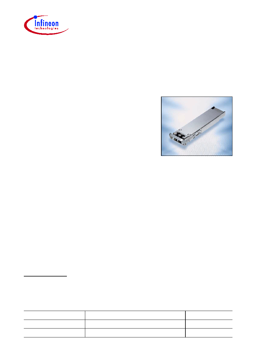
XFP
850 nm Small Form Factor Module
10 Gigabit Pluggable Transceiver
Compatible with XFP MSA Rev. 3.1
V23833-F0005-B101
V23833-F0005-B102
Preliminary Data Sheet
Fiber Optics
Ordering Information
Part Number
Chassis/Signal Grounding Concept
Standard
V23833-F0005-B101
Separated
Multi-Protocol
V23833-F0005-B102
Common
Multi-Protocol
File: 2115
Features
Standards
∑ Compatible with IEEE 802.3aeTM-2002
∑ Compatible with Fibre Channel 10GFC Draft 3.5
∑ Compatible with XFP MSA Rev. 3.1
Optical
∑ IEEE Ethernet: Serial 850 nm 10GBASE-SR
∑ T11 Fibre Channel: Serial 850 nm
1200-M5-SN-I; 1200-M5E-SN-I; 1200-M6-SN-I
∑ Transmission distance
≠ up to 82 m
1)
(50 µm MMF)
≠ up to 300 m
1)
(on special MMF)
∑ Vertical Cavity Surface Emitting Laser at 850 nm (VCSEL)
∑ LC connector, multimode fiber
∑ Full duplex transmission mode
1)
Maximum reach as defined by IEEE. Longer reach possible depending upon link implementation.

V23833-F0005-B101
V23833-F0005-B102
Applications
Preliminary Product Information
2
2004-06-16
Monitoring and Control
∑ Laser safety shut off
∑ Supply voltage 5 V / 3.3 V
∑ Transmit power
∑ Received power RSSI
∑ Laser bias current
∑ Tx_DIS
∑ Mod_NR
∑ Mod_DeSel
∑ Interrupt
∑ Mod_ABS
∑ P_Down/RST
∑ Rx_Los
Mechanical
∑ Color coded beige for 850 nm
∑ Belly-to-belly applications
∑ Latching mechanism with low insertion force
Electrical
∑ Hot pluggable
∑ Power supply 5 V / 3.3 V only
∑ Total power consumption < 1.5 W max.
∑ XFI electrical interface
∑ Reference clock not required
∑ Management and control via 2-wire interface
∑ 30 pin connector, 0.8 mm pitch
Applications
∑ 10GBE, 10GFC and G.709 transmission systems for short range
∑ Integration on PCI card, with eventually mid-board mounting
∑ Belly-to-belly for high density applications
∑ Enterprise and campus network applications
∑ Storage applications
∑ Backplane and switch applications
∑ Aggregation point for lower date rate
∑ XFP evaluation kit V23833-F9909-Z001 available upon request
V23833-F0005-B101
V23833-F0005-B102
Pin Configuration
Preliminary Product Information
3
2004-06-16
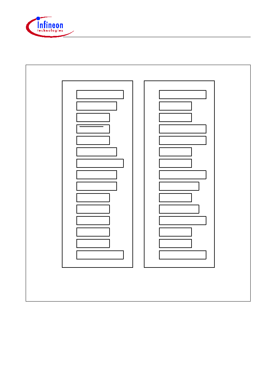
Pin Configuration
Figure 1
XFP Transceiver Electrical Pad Layout
File: 2304
1
2
3
4
5
6
7
8
9
10
11
12
13
14
15
GND
V
EE5
MOD_DESEL
INTERRUPT
TX_DIS
V
CC5
GND
V
CC3
V
CC3
SCL
SDA
MOD_ABS
MOD_NR
RX_LOS
GND
30
29
28
27
26
25
24
23
22
21
20
19
18
17
16
GND
TD+
TD
-
GND
GND
REFCLK
-
REFCLK+
GND
V
CC2
P_DOWN/RST
V
CC2
GND
RD+
RD
-
GND
Bottom of Board
(As viewed through top of board)
Top of Board

V23833-F0005-B101
V23833-F0005-B102
Pin Configuration
Preliminary Product Information
4
2004-06-16
Connector Pin Assignments
Pin No.
Signal Name
Pin No.
Signal Name
1
GND
30
GND
2
V
EE5
29
TD+
3
MOD_DESEL
28
TD≠
4
INTERRUPT
27
GND
5
TX_DIS
26
GND
6
V
CC5
25
REFCLK≠
7
GND
24
REFCLK+
8
V
CC3
23
GND
9
V
CC3
22
V
CC2
10
SCL
21
P_DOWN
11
SDA
20
V
CC2
12
MOD_ABS
19
GND
13
MOD_NR
18
RD+
14
RX_LOS
17
RD≠
15
GND
16
GND

V23833-F0005-B101
V23833-F0005-B102
Pin Configuration
Preliminary Product Information
5
2004-06-16
Pin Description
Signal Name
Level
I/O
Pin No.
Description
Management and Monitoring Ports
MOD_DESEL
LVTTL
I
3
Module De-select: when "L" allows
the module to respond to 2-wire
serial interface command. "H" active
INTERRUPT
LVTTL
O
4
Interrupt: indicates presence of an
important condition which can be
read on the 2-wire serial interface.
"H" active
TX_DIS
LVTTL
I
5
Transmitter Disable: transmitter
laser source is turned off. "H" active
SCL
LVTTL
I
10
2-wire Interface Clock
SDA
LVTTL
I
11
2-wire Interface Data
MOD_ABS
LVTTL
O
12
Module Absent: indicating the
modules not present. "H" active
MOD_NR
LVTTL
O
13
Module not ready: module
operational fault
RX_LOS
LVTTL
O
14
Receiver Loss Of Signal Indicator
P_DOWN
LVTTL
I
21
Power Saving Mode: places the
module in the stand-by condition.
Active "H". During the falling edge
set the module reset
Transmit Functions
TD≠
CML
I
28
Transmitter Inverted Data Input
TD+
CML
I
29
Transmitter Not-inverted Data Input
Receive Functions
RD≠
CML
O
17
Receiver Data Output Inverted
RD+
CML
O
18
Receiver Data Output Not-inverted
REFCLK+
PECL
I
24
Reference Clock Not-inverted
Input
1)
REFCLK≠
PECL
I
25
Reference Clock Inverted Input
1)