 | –≠–ª–µ–∫—Ç—Ä–æ–Ω–Ω—ã–π –∫–æ–º–ø–æ–Ω–µ–Ω—Ç: IL2010BD | –°–∫–∞—á–∞—Ç—å:  PDF PDF  ZIP ZIP |
IL2010B
Korzhenevskogo 12, Minsk, 220108, Republic of
Belarus
Fax: +375 (17) 278 28 22,
Phone: +375 (17) 278 07 11, 212 24 70, 212 24 61,
212 69 16
E-mail: office@bms.by
URL: www.bms.by
P
HASE
C
ONTROL
C
IRCUIT FOR
C
URRENT
F
EEDBACK
Description
The IL2010B is designed as a phase-control
circuit in bipolar technology. It enables load-
current detection and has a soft-start function as
well as reference voltage output. Motor control
with load-current feedback and overload
protection are preferred applications.
Features
û
Full wave current sensing
û
Mains supply variation compensated
û
Programmable load-current limitation
with over- and high-load output
û
Variable soft-start
û
Voltage and current synchronization
û
Automatic retriggering switchable
û
Triggering pulse typical 125 mA
û
Internal supply voltage monitoring
û
Current requirement
ò
3 mA
û
Temperature compensated reference voltage
Applications
û
Advanced motor control
û
Grinder
û
Drilling machine
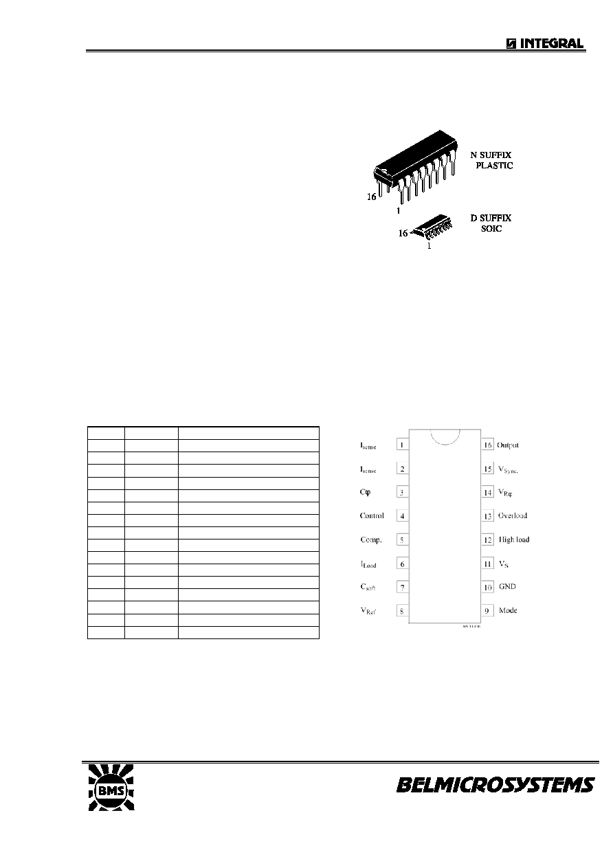
Pin Description
Pin Symbol Function
1 I
sense
Load current sensing
2 I
sense
Load current sensing
3
C
Ramp voltage
4 Control
Control
input
5 Comp.
Compensation
output
6 I
Load
Load current limitation
7 C
soft
Soft
start
8 V
Ref
Reference
voltage
9 Mode Mode
selection
10 GND Ground
11 V
S
Supply
voltage
12
High load High load indication
13 Overload
Overload
indication
14
V
R
Ramp current adjust
15 V
Sync.
Voltage
synchronization
16 Output Trigger
output

IL2010B
Korzhenevskogo 12, Minsk, 220108, Republic of
Belarus
Fax: +375 (17) 278 28 22,
Phone: +375 (17) 278 07 11, 212 24 70, 212 24 61,
212 69 16
E-mail: office@bms.by
URL: www.bms.by
Block Diagram
Absolute Maximum Ratings
Reference point Pin 10, unless otherwise specified
Parameters Pin
Symbol
Value Unit
-I
S
30
mA
Sink current
t
ò10us
11
-i
s
100
I
syncV
5 mA
Sync. currents
t
ò10us
15
i
syncV
20
Phase control
Control voltage
4 and 8
-V
I
0 - V
8
V
Input current
4
I
I
500 uA
Charging current
14
- I
max
0.5 mA
Soft-start
Input voltage
7 and 8
-V
I
0 - V
8
V
Pulse output
+V
I
2
Input voltage
16
-V
I
V
11
V
Reference voltage source
I
0
10
mA
Output current
t
ò10us
8
i
0
30
mA
Load current sensing
Input currents
1 and 2
I
i
1 mA
Input voltages
5 and 6
- V
i
0 - V
8
V
Overload output
13
I
L
1
mA
I
L
30
mA
High-load output
t
ò10us
12
i
L
100
mA
Storage temperature range
T
stg
-40 to +125
o
C
Junction temperature range
T
j
125
o
C
Ambient temperature range
T
amb
-10 to +100
o
C

IL2010B
Korzhenevskogo 12, Minsk, 220108, Republic of
Belarus
Fax: +375 (17) 278 28 22,
Phone: +375 (17) 278 07 11, 212 24 70, 212 24 61,
212 69 16
E-mail: office@bms.by
URL: www.bms.by
Electrical Characteristics
V
S
=-13 V, Tamb = 25
o
C, reference point Pin 10, unless otherwise specified
Parameters Test
Conditions
Pins
Symbol
Min.
Typ.
Max.
Unit
Supply
-I
S
= 5.5 mA
14.5
16.5
Supply voltage limitation
-I
S
= 30 mA
11 -V
S
14.6 16.8
V
Current requirement
-V
S
= 13.0 V
(Pins 1, 2, 8 and 15 open) Pin 11
-I
S
5.2
mA
Reference voltage source
I
L
= 10 uA
8.7
9.0
9.3
Reference voltage
I
L
= 2.5 mA
-V
Ref
8.5 8.8 9.2
V
I
S
= 2.5 mA
-0.004
Temperature coefficient
I
S
= 10 uA
8
TC
VRef
+0.006
%/K
Voltage monitoring
Turn-on threshold
11
-V
Son
11.3
12.3 V
Phase control - synchronization
Voltage limitation
I
L
= 2 mA
V
syncV
8.0 8.5 9.0 V
Input current
Current sync.
16
I
syncI
3 30
uA
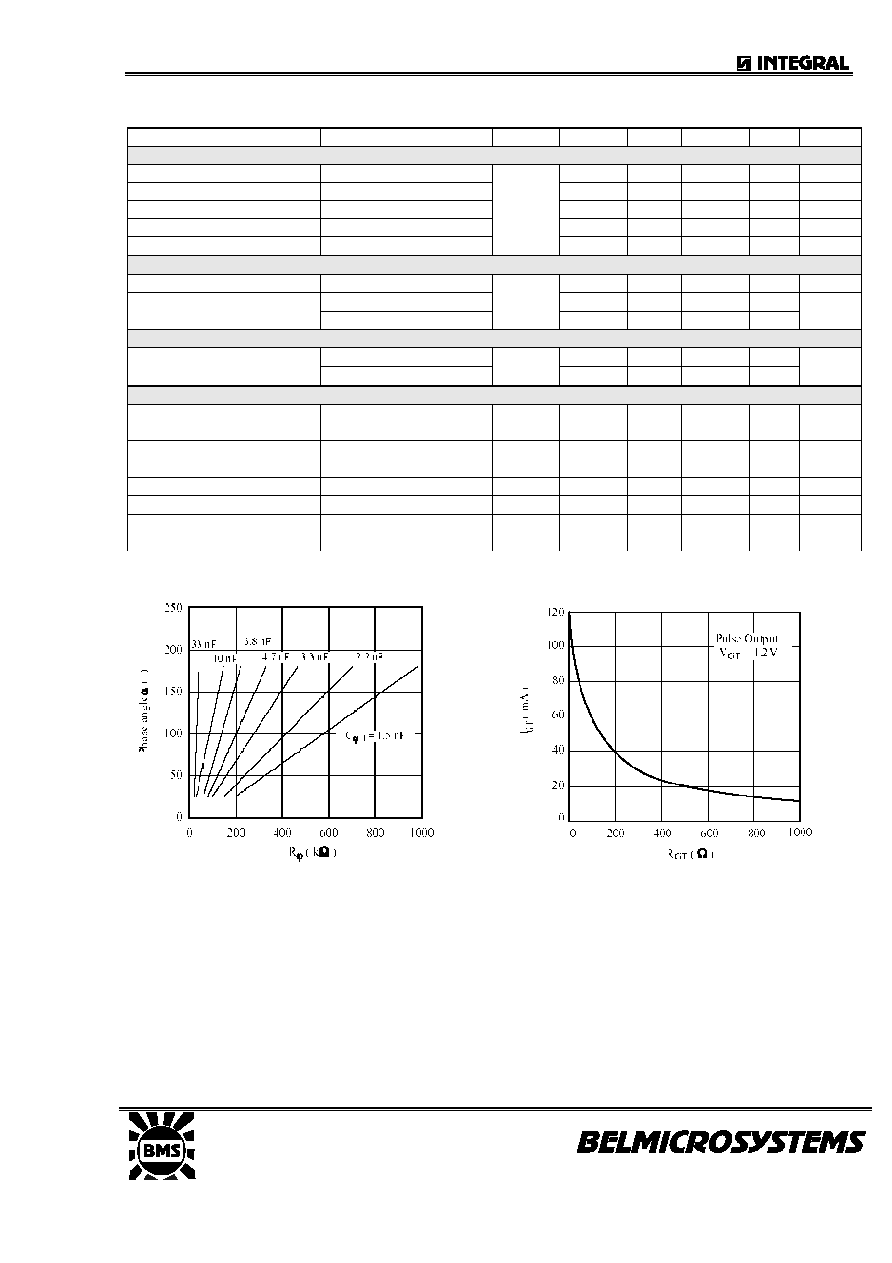
Reference ramp, fig. 1
Charging current
14
-I
1
100
uA
Start voltage
3
-V
max
2.00 2.15 2.20 V
Temperature coefficient of
start voltage
3 TC
R
-0.003
%/K
Final voltage
3 -V
min
(V
8
200 mV)
R
reference voltage
I
=10uA
14 and
11
V
R
0.96 1.02 1.10 V
I
=10 uA
0.03
Temperature coefficient
I
=1 uA
14
TC
VR
0.06
%/K
Pulse output current
V
16
= - 1.2 V, fig. 2,
16
I
0
100 125
150
mA
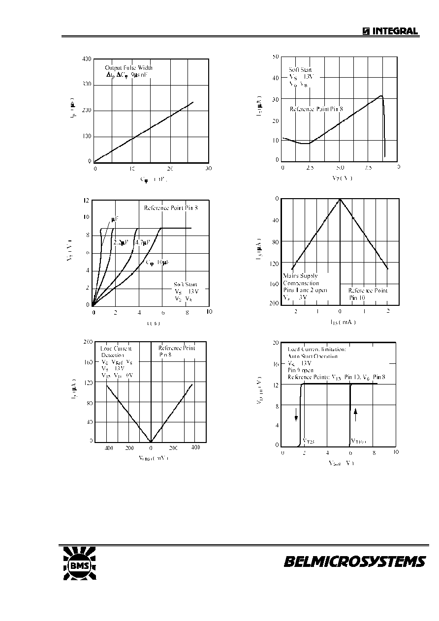
Output pulse width
C
3
= 3.3 nF, fig. 3
16
t
p
50 us
Automatic retriggering
Repetition rate
I
15
=150 uA
t
pp
3 5 7.5
t
p
Threshold voltage
16
V
I
20 100
mV
Soft start, figure 7 and 8
Starting current
V
7
= V
8
7
-I
0
5 10 20
uA
Final current
V
7-10
= -1V
-I
0
20 25 50 uA
Discharge current
+I
0
0.5
mA
Output current
4
+I
0
0.2 2 mA
Supply voltage compensation,
Transfer gain
fig. 6 I
15
/ I
5
Pin 15/5
(Pins 1 and 2 open)
G
i
12 18
Output offset current
V
(R6)
= V
15
= V
5
= 0
I
0
2
uA
Load current detection
,
R
1
= R
2
= 3 k
, V
15
= 0, V
5
= V
6
= V
8
, fig. 7
Transfer gain
I
5
/150 mV, I
6
/150 mV
G
I
0.28 0.32
0.37
uA/mV
Output offset currents
5, 6 - 8
-I
0
0 3 6 uA
Reference voltage
I
1
, I
2
= 100 uA
1 and 2
-V
Ref
300
450 mV
Shunt voltage amplitude
V
(R6)
250
mV
IL2010B
Korzhenevskogo 12, Minsk, 220108, Republic of
Belarus
Fax: +375 (17) 278 28 22,
Phone: +375 (17) 278 07 11, 212 24 70, 212 24 61,
212 69 16
E-mail: office@bms.by
URL: www.bms.by
Parameters Test
Conditions
Pins
Symbol
Min.
Typ.
Max.
Unit
Load current limitation figs. 8 to 13
High load switching
Threshold V
T70
V
T70
4 4.35
4.7 V
Overload switching
Threshold V
T100
V
T100
5.8 6.2 6.6 V
Restart switching
Threshold V
T25
V
T25
1.25 1.55 1.85 V
Input current
Enquiry mode
I
i
1
uA
Output impedance
Switching mode
6-8
R
0
2 4 8 k
Programming input
Input voltage - auto-start
Pin 9 open
-V
9
3.8 4.3 4.7 V
V
9
= 0 (
max
)
-I
9
5 10 20
Input current
V
9
= V
8
(I
max
)
9
I
9
5 10
20
uA
High load output, V
T70
, fig. 9, I
12
= -3 mA,
V
6-8
ò
V
T70
V
sat
0.5 0.75 1.0
Saturation voltages
V
6-8
ô
V
T70
11-12
V
lim
7.3 8.1
V
Overload output, V
T100
, V
9
= open or V
9
= V
10
, fig. 10
V
6-8
ô
V
T25
Leakage current
V
13
= (V
11
+1)V 13
I
lkg
0.5
uA
V
6-8
ô
V
T100
,
Saturation voltages
I
13
= 10 uA
11-13
V
sat
0.15
V
Output current, max. load
V
9
= V
8
, fig. 10
13
I
13
1
mA
Leakage current
V
6
ò V
T100
13 I
lkg
4
uA
Output impedance
Open collector
V
6
ò V
T100
13 R
0
2 4 8 k
Fig.1
Fig.2
IL2010B
Korzhenevskogo 12, Minsk, 220108, Republic of
Belarus
Fax: +375 (17) 278 28 22,
Phone: +375 (17) 278 07 11, 212 24 70, 212 24 61,
212 69 16
E-mail: office@bms.by
URL: www.bms.by
Fig.3
Fig.4
Fig.5
Fig.6
Fig.7
Fig.8