IL33153
1
S
INGLE
IGBT
G
ATE
D
RIVER
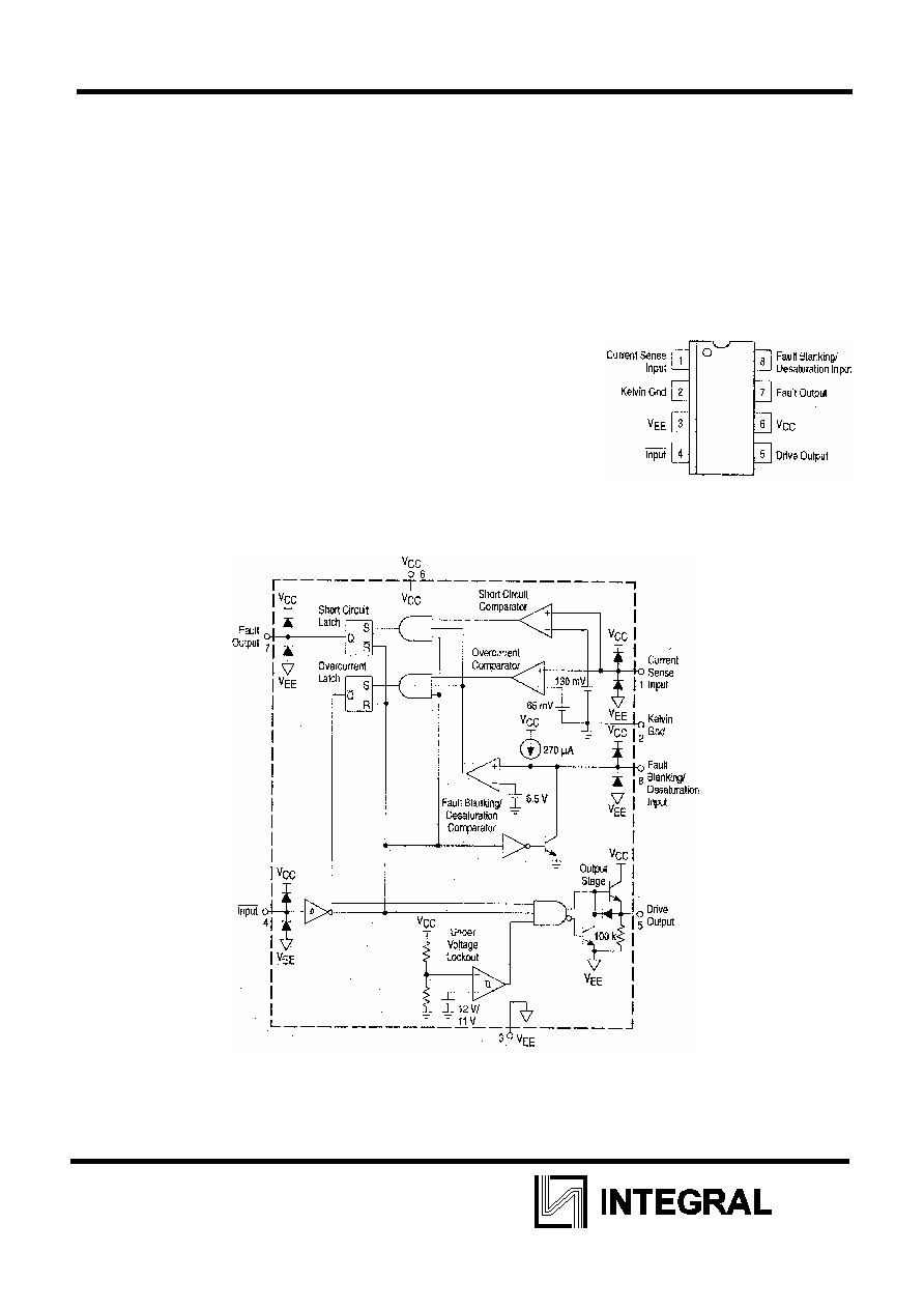
The IL33153 is specifically designed as an IGBT driver for high power applications that include ac
induction motor control, brushless dc motor control and uninterruptable power supplies. Although
designed for driving discrete and module IGBTs, this device offers a cost effective solution for driving
power MOSFETs and Bipolar Transistors. Device protection features include the choice of
desaturation or overcurrent sensing and undervoltage detection. These devices are available in dual-
inline and surface mount packages and include the following features:
F
EATURES
û High Current Output Stage: 1.0 A Source/2.0 A Sink
û Protection Circuits for Both Conventional and Sense IGBTs
û Programmable Fault Blanking Time
û Protection against Overcurrent and Short Circuit
û Undervoltage Lockout Optimized for IGBT's
û Negative Gate Drive Capability
û Cost Effectively Drives Power MOSFETs and Bipolar Transistors
B
LOCK
S
CHEME
IL33153
2
A
BSOLUTE MAXIMUM RATINGS
Rating Symbol
Value
Unit
Power Supply Voltage
V
CC
to
V
EE
Kelvin Ground to
V
EE
(Note 1 )
V
CC
-
V
EE
KGnd -
V
EE
20
20
V
Logic Input
Vin
V
EE
-O,3 to V
CC
V
Current Sense Input
V
S
-0.3 to Vcc
V
Blanking/Desaturation Input
V
BD
-0.3 to Vcc
V
Gate Drive Output
Source Current
Sink Current
Diode Clamp Current
I
O
1.0
2.0
1.0
A
Fault Output
Source Current
Sink Curent
I
FO
25
10
mA
Power Dissipation and Thermal Characteristics
D Suffix SO-8 Package, Case 751
Maximum Power Dissipation @ T
A
= 5O
úC Thermal
Resistance, Junction-to-Air
P Suffix DIP-8 Package, Case 626
Maximum Power Dissipation @ T
A
= 5O
úC Thermal
Resistance, Junction-to-Air
P
D
R
JA
P
D
R
JA
0.56
180
1.0
100
W
úC/W
W
úC/W
Operating Junction Temperature
T
J
+150
úC
Operating Ambient Temperature
T
A
-40 to +105
úC
Storage Temperature Range
Tstg
-65 to +150
úC
IL33153
3
ELECTRICAL CHARACTERISTICS
(
Vcc=15V, V
EE
=0V, Kelvin Gnd connected to V
EE
. For typical values
T
A
=25
úC, for min/max values T
A
is the operating ambient temperature range that applies (Note 2), unless otherwise noted.)
Characteristic Symbol
Min
Typ
Max
Unit
LOGIC INPUT
Input Threshold Voltage ]
High State (Logic 1 )
Low State (Logic 0)
V
IH
V
IL
-
1.2
2.70
2.30
3.2
-
V
Input Current
High State (
V
IH
= 3.0 V)
Low State (V
ii
. = 1.2 V)
I
IH
I
IL
-
-
130
50
500
100
A
DRIVE OUTPUT
Output Voltage
Low State (Isink = 1.0 A)
High State (Isource = 500 mA)
V
OL
V
OH
-
12
2.0
13.9
2.5
-
V
Output Pull-Down Resistor
R
PD
-
100
200
k
FAULT OUTPUT
Output voltage
Low Slate (Isink = 5.0 mA)
High State (Isource = 20 mA)
V
FL
V
FH
-
12
0.2
13.3
1.0
-
V
SWITCHING CHARACTERISTICS
Propagation Delay (50% Input to 50% Output C
L
= 1.0 nF)
Logic Input to Drive Output Rise
Logic Input to Drive Output Fall
t
PLH
(in/out) t
PHL
(in/out)
-
-
80
120
300
300
ns
Drive Output Rise Time (10% to 90%) C
L
= 1.0 nF
tr
-
17
55
ns
Drive Output Fall Time (90% to 10%) C
L
= 1.0 nF
tf
-
17
55
ns
Propagation Delay
Current Sense Input to Drive Output
Fault Blanking/Desaturation Input to Drive Output
tp
(OC)
tp
(FLT)
-
-
0.3
0.3
1.0
1.0
s
UVLO
Startup Voltage
V
SS
S
tart 11.3
12 12.6
V
Disable Voltage
V
SS
dis 10.4
11
11.7
V
COMPARATORS
Overcurrent Threshold Voltage (V
pin8
> 7,0 V)
V
SOC
50 65 80 mV
Short Circuit Threshold Voltage (V
pine8
> 7,0 V)
V
SSC
100 130 160 mV
Fault Blanking/Desaturation Threshold (Vpin1 > 100 mV)
V
th(FLT
)
6.0 6.5 7.0 V
Current Sense Input Current (Vsi = 0 V)
I
SI
-
-1.4
-10
mA
FAULT BLANKING/DESATURATION INPUT
Current Source (Vpjn8 = 0 V, Vpin4 = 0 V)
Ichg
-200
-270
-300
mA
Discharge Current (Vpin8 = 15 V, Vpin4 = 5.0 V)
Idschg
1.0
2.5
-
mA
TOTAL DEVICE
Power Supply Current
Standby (Vpin 4 =
V
CC
,
O
utput Open)
Operating (C
L
=
1.0 nF, f= 20 kHz)
I
CC
-
-
7.2
7.9
14
20
mA
NOTES: 1. Kelvin Ground must always be between
V
EE
and
V
CC
.
2.Low duty cycle pulse techniques are used during test to maintain the junction temperature as close
to ambient as possible.
Tlow = -40úC lor IL33153
Thigh = +105
úClor IL33153