 | –≠–ª–µ–∫—Ç—Ä–æ–Ω–Ω—ã–π –∫–æ–º–ø–æ–Ω–µ–Ω—Ç: IL33193D | –°–∫–∞—á–∞—Ç—å:  PDF PDF  ZIP ZIP |
TECHNICAL DATA
IL33193
Automotive Direction Indicator
ORDERING INFORMATION
IL33193N
DIP
IL33193D
SOIC
T
A
= -40
ú to 125úC for all packages
The IL33193 is a new generation industry standard UAA1041 "Flasher".
It has been developed for enhanced EMI sensitivity, system reliability, and
improved wiring simplification. The IL33193 is pin compatible with the
UAA1041 and UAA1041B in the standard application configuration as shown
in Figure 9, without lamp short circuit detection and using a 20 m
shunt
resistor. The IL33193 has a standby mode of operation requiring very low
standby supply current and can be directly connected to the vehicle's battery.
It includes an RF filter on the Fault detection pin (Pin 7) for EMI purposes.
Fault detection thresholds are reduced relative to those of the UAA1041,
allowing a lower shunt resistance value (20 mW) to be used.
û Pin Compatible with the UAA1041
û Defective Lamp Detection Threshold
û RF Filter for EMI Purposes
û Load Dump Protection
û Double Battery Capability for Jump Start
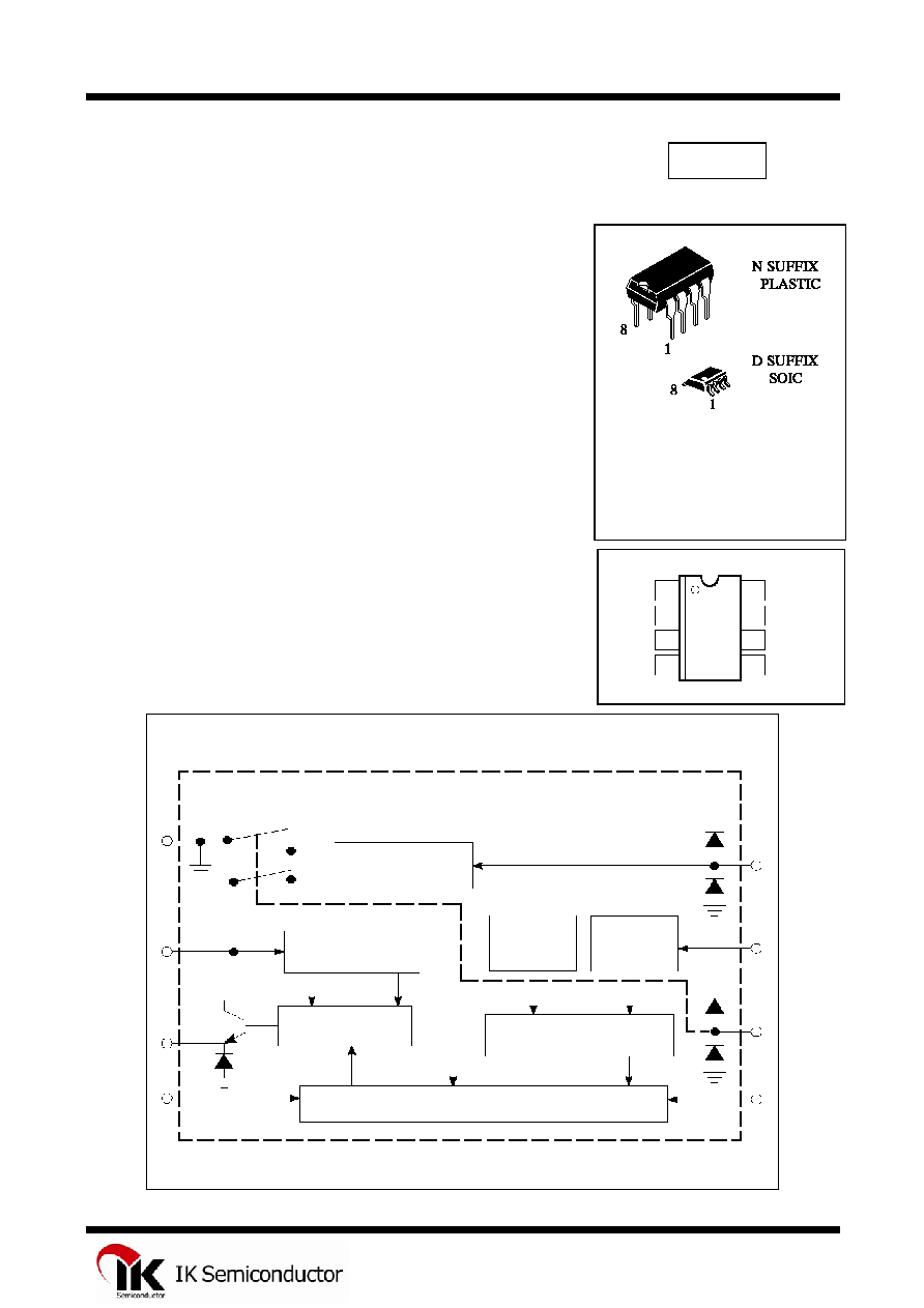
PIN CONNECTIONS
1
2
3
4
5
6
7
8
Vss
Oscillator
Oscillator
VÒÒ
Relay
Starter
Fault
Detector
Enable
1
2
3
4
5
6
7
8
Oscillator
Lamp Fault
Detector
RF
Filter
Reference
Voltage
Relay
Driver
Detector
24V
33V
Starter
SW1
SW2
Simplified Block Diagram
This Device contains 60 active transistors.
1

IL33193
MAXIMUM RATINGS
*
Rating Simbol
Value
Unit
Pin1 Positive Current (Continious/Pulse)
I1+
150 to 500
mA
Pin1 Negative Current (Continious/Pulse)
I1-
-35 to -500
mA
Current (Continious/Pulse)
I2
350 to 1900
mA
Current (Continious/Pulse)
I3
300 to 1400
mA
Current (Continious/Pulse)
I8
25 to 50
mA
ESD(Aii Pins Except Pin4 for Negative Pulse)
V
ESD
2000
úV
ESD(Pin 4 Negative Pulse)
V
ESD4-
-1000
úV
Jinction Temperature
T
J
150
úC
Operation Ambient Temperature Range
T
A
-40 to +125
úC
Storage Temperature Range
T
STG
-65 to +150
úC
ELECTRICAL CHARACTERISTICS
(-45
O
C
ò T
A
ò +125
O
C, 8.0 V
ò V
CC
ò 18.0 V, unless otherwise noted.
Typical values reflect approximate mean at T
A
= 25
O
C, V
CC
= 14 V at the time of initial device characterization.)
Characteristic Symbol
Min
Max
Unit
Battery Voltage Range (Normal Operation)
V
b
8.0 18 V
Overvoltage Detector Threshold (V
Pin2
- V
Pin1
) V
ih
19 22 V
Clamping Voltage (R2 = 220
)
V
cl
27 34 V
Output Voltage [I = -250 mA (V
Pin2
- V
Pin3
)] V
sat
- 1.5 V
Starter Resistance (R
st
= R2 +R
Lamp
) R
st
- 3.6 k
Oscillator Constant (Normal Operation, T
A
= 25
O
C) K
n
1.3 1.75
Temperature Coefficient of K
n
TC
Kn
- - 1/
O
C
Duty Cycle (Normal Operation)
-
45
55
%
Oscillator Constant (One 21 W Lamp Defect, T
A
= 25
O
C) K
f
0.59 0.75
Duty Cycle(One 21 W Lamp Defect)
-
35
45
%
Oscillator Constant (T
A
= 25
O
C) K1
K2
0.150
0.200
0.240
0.290
Standby Current (Ignition Off)
I
CC
- 100
A
Current Consumption (Relay Off, Enable Pin 6 High)
V
bat
= 13.5 V, R3 = 220
I
CC
- 3.5 mA
Current Consumption (Relay On)
V
bat
= 13.5 V, R3 = 220
I
CC
- 6.0 mA
Defect Lamp Detector [R3 = 220
, (V
Pin2
- V
Pin7
)]
V
bat
= 13.5 V
V
S
42.5 56 mV
2

IL33193
t1
tn
Fn=1/tn
TIME
Vbat
On Off
tf
Ft=1/tf
On
TIME
Vbat
Off
Figure 1 - Normal Operation Oscillator
Figure 2 - One Defective Lamp Oscillator
Timing
Diagram
Timing
Diagram
INTRODUCTION
The IL33193 is designed to drive the direction indicator flasher relay. It is a new generation industry standard
UAA1041 "Flasher". It consists of the following functions:
û Supply and Protections
û On-Chip Relay Driver
û Oscillator
û Starter Functions
û Lamp Fault Detector with Internal RF Filter
û Standby Mode
Supply and Protection Systems
Pin 1 is connected to ground via resistor R3 which limits he current in the event of any high voltage transients. Pin 2
(VCC) is the positive supply and may be connected directly to the vehicle's battery voltage. Overvoltage and Double
Battery Protection: When the applied VCC to VSS voltage is greater than 22 V, the overvoltage detector circuit turns
the relay driver off. Both the device and the lamps are protected if two 12 V batteries are connected in series and used
to jump start the vehicle.Load Dump Overvoltage Protection: A 29 V overvoltage detector protects the circuits against
high voltage transients due to load dumps and other low energy spikes. The relay driver is automatically turned on
whenever the VCC to VSS voltage is greater than 34 V. Overvoltage Protection, High Voltage Transients: The Enable
and the Starter pins are protected against positive and negative transients by internal on-chip diodes.
On-Chip Relay Driver
The device directly drives the flasher relay. The output structure is an Emitter of an NPN transistor. It contains the
free wheeling diode circuitry necessary to protect the device whenever the relay is switched off.
Oscillator
The device uses a sawtooth oscillator (Figure 1). The frequency is determined by the external components C1 and R1.
In the normal operating mode, the flashing frequency is: Fn = 1/R1*C1*Kn. With a defective (open) 21 W
lamp (Figure 2), the flashing frequency changes to: Fn = 2.2*Fn.
The typical first flash delay (the time between the moment when the indicator switch is closed and the first lamp flash
occurs) is: t1 = K1*R1*C1 The fault detection delay is from the time relay R1 is on and fault detection is enabled.
Where a 21 W lamp opens, the delay is expressed as: t2 = K2*R1*C1
3

IL33193
Starter
Pin 8 is connected through a 3.3 kW resistor to the flashing lamp. Pin 8 is the input to the Starter function and senses
the use of S1 by sensing ground through the lamp (Figures 9 and 10).
Lamp Fault Detector with Internal RF Filter
A Lamp defect is sensed by the lamp fault detector's monitoring of the voltage developed across the external shunt
resistor RS via the RF filter. The RS voltage drop is compared to a Vbat dependent internal reference voltage (Vref) to
validate the comparison over the full battery voltage range. A detected fault causes the oscillator to change frequency
(Figure 2).
Standby Mode
When the ignition key and warning switches are open; Enable is in a low state and the internal switches, SW1 and
SW2, are open and no current passes through the circuit. In this condition, the device's current consumption is zero
(ICC = 0). When ignition key and warning switches are closed; Enable is in a high state with SW1 and SW2 being
closed and the circuit is powered on.
Main differences between UAA1041B & IL33193
The IL33193 is pin compatible with the UAA1041.
Supply Current
Supply current is more stable on the IL33193 when the device is in "on" or "off" state. In "on" state the supply current
is only 40% higher than when in the "off" state, as compared to a ratio of 3 times for the UAA1041. This results in a
lowern voltage drop across the ground resistor R3 (see On-Chip Relay Driver).
Short Circuit Detection
The IL33193 has no short circuit detection.
Standby Mode (Pin 6)
The UAA1041 has no standby mode. Pin 6 is used as an Enable/Disable for the short circuit detection. The IL33193
uses Pin 6 to set the device in standby mode. If Pin 6 is connected to ground, the IL33193 is in the standby mode. In
this mode, standby current is very low and Pin 8's starter resistor R2 and a 2.0 kW internal resistor are switched off. As
soon as Pin 6 is at a high level (typical threshold = 2Vbe) the device becomes active. In the application, the IL33193
can be connected directly to the battery and awakened whenever Pin 6 is connected to the vehicle's battery by way of a
protection resistor and the ignition key switch.
Lamp Defect Detection (Pin 7)
The UAA1041 operates with a 30 mW shunt resistor to sense the lamp current. It's lamp defect detection threshold of
Pin 7 is typically 85 mV. The IL33193 is designed to operate with 20 mW shunt resistor and at a reduced threshold of
50 mV. This reduces power generation in the flasher module. In addition, the IL33193 incorporates an RF filter to
enhance RFI immunity.
Load Dump and Overvoltage Behavior
The UAA1041 and IL33193 both behave the same in this regard. Both have double battery detection and lamp turn-off
protection in the event of a jump start. During load dump, both devices are protected by an internal 30 V zener diode
with the relay activated during a load dump.
Relay Driver
Drive capability of both devices is the same. Free wheeling diode protection is internal to both devices. The free
wheeling voltage is 2Vbe for the UAA1041 and 3Vbe for the IL33193. This results in a higher clamp voltage across the
relay and thus in a faster turn-off. In addition, the lower "on" state supply current is lower on the IL33193 and thus the
voltage drop across the ground resistor R3 is reduced. This results in an even higher clamp voltage across the relay.
Oscillator Phase
The oscillator phase is opposite on the IL33193 as compared to the UAA1041. The Oscillator voltage is falling
during "on" state and rising during "off" state for the IL33193.
4

IL33193
V
cl
, CLAMPING VOLTAGE (V)
V
ih
, OVERVOLTAGE DETECT THRESHOLD (V)
T
A
, AMBIENT TEMPERATURE (
O
C) T
A
, AMBIENT TEMPERATURE (
O
C)
Figure 3 - Clamping Voltage versus Temperature
Figure 4 - Overvoltage Detector versus Temperature
I
CC
, SUPPLY CURRENT (mA)
V
sat
, OUTPUT VOLTAGE (V)
Vbat = 13.5B
R2 = 220
Relay
Relay Off
Vbat = 13.5V
I = 250 mA
T
A
, AMBIENT TEMPERATURE (
O
C) T
A
, AMBIENT TEMPERATURE (
O
C)
Figure 5 - Supply Current versus Temperature
Figure 6 - Output Voltage versus Temperature
LAMP DEFECT DETECTION THRESHOLD (mV)
K
f
, OSCILLATOR CONSTANT (TIMES)
Vbat = 13.5V
R2 = 220
T
A
, AMBIENT TEMPERATURE (
O
C) T
A
, AMBIENT TEMPERATURE (
O
C)
Figure 7 - Defect Lamp Detection versus Temperature
Figure 8 - Oscillator Constant versus Temperature
5