 | –≠–ª–µ–∫—Ç—Ä–æ–Ω–Ω—ã–π –∫–æ–º–ø–æ–Ω–µ–Ω—Ç: IL5851N | –°–∫–∞—á–∞—Ç—å:  PDF PDF  ZIP ZIP |

TECHNICAL DATA
IL5851
PULSE DIALER WITH REDIAL
The IL5851 is a monolithic CMOS integrated circuit which uses an
inexpensive RC oscillator for its frequency reference and provides all the
features required for implementing a pulse dialer with 32 digit redial.
ORDERING INFORMATION
IL5851N Plastic
T
A
= -20
ú to 70ú C
û
Wide operating voltage range (2.0~6.0V)
û
Low power dissipation
û
Use either a standard 2 of 7 matrix keyboard with negative true common
or the inexpensive form A-type keyboard
û
Make/Break ratio can be selected
û
Redial with * or #
û
Continuous MUTE
û
Power up clear circuitry on chip
û
10 pps/20 pps can be selected
PIN ASSIGNMENT
LOGIC DIAGRAM
PIN 1 = V
CC
PIN 6 = GND
1
IL5851
PIN DESCRIPTION
NAME PIN
DESCRIPTION
V
CC
1
Positive supply pin.
The voltage on this pin is measured relative to Pin 6 and is supplied from a
150
A current source. This voltage should be regulated to less than 6.0 volts
using on external form or regulation.
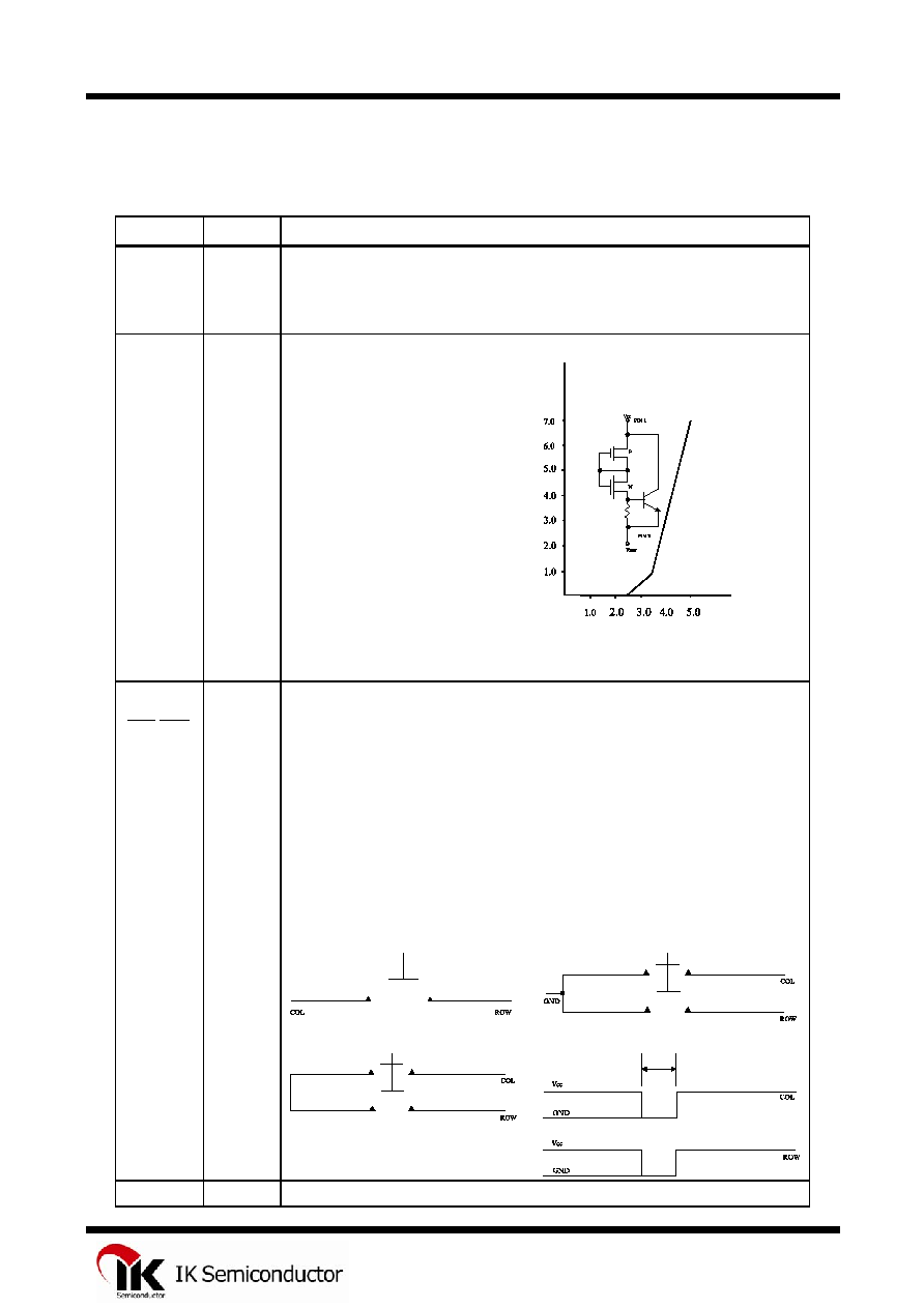
V
REF
2 The
V
REF
output provides reference
voltage that tracks internal
parameters of the IL5851N. V
REF
provides a negative voltage reference
to the V
CC
supply. Its magnitude will
be approximately 0.6 volt higher than
the minimum operating voltage of
each particular IL5851N.
The typical application would be to
connect the V
REF
pin to the GND pin
(Pin 6). The supply to the V
CC
pin
(Pin 1) should then be regulated to
150
A (I
OP
max). with this amount of
supply current, operation of the
IL5851N is guaranteed.
The internal circuit of the V
REF
function is shown in Figure 1 with its
associated I-V characteristic
.
___ _____
Row1-Row4,
Col1-Col4
3,4,5,13,
14,15,16
Keyboard inputs.
The IL5851N incorporates an innovative keyboard scheme that allows either the
standard 2-of-7 keyboard with negative common or the inexpensive single
contact (form A) keyboard to be used.
A valid key entry is defined by either a single row being connected to a single
column or GND being simultaneously presented to both a single row and column.
When in the on-hook mode, the row and column inputs are held high and no
keyboard inputs are accepted.
When off-hook, the keyboard is completely static until the initial valid key input
is sensed. The oscillator is then enabled and the rows and columns are scanned
alternately (pulled high, then low) to verify the varied input. The input must
remain valid for 10msec of debounce time to be accepted.
Form A type keyboard
2 of 7 keyboard (negative common)
2 of 7 keyboard
Electronic input
GND 6
Negative
supply
2

IL5851
pin is connected to the common part in general applications.
RC1-RC3 7,8,9 Oscillator
The IL5851N contains on-chip inverters to provide oscillator which will operate
with a minimum external components.
Following figure shows the on-chip configuration with the necessary external
components. Optimum stability occurs with the ration K=R
S
/R equal to 10
The oscillator period is given by:
T=RC(1.386+(3.5KC
S
)/C-(2K/(K+1)) in (K/(1.5K + 0.5))
Where C
S
is the stray capacitance on Pin 7.
Accuracy and stability will be enhanced with this capacitance minimized.
PPS 10
10/20pps
Select
Connecting this pin to GND (pin 6) will select an output pulse rate of 10pps.
Connecting the pin V
CC
(pin 1) will select an output pulse rate of 20pps.
M/B 11
Make/break
Select
The Make/Break pin controls the Make/Break ratio of the pulse output. The
make/Break ratio is controlled by connection V
CC
or GND to this pin as shown in
the following table.
Input
Make
Break
V
CC
(Pin1) 33.4%
66.6%
GND(PIn
6)
40%
60%
____
Mute
12 Mute
Output
The mute output is an open-drain N-Channel transistor designed to drive external
bipolar transistor.
This circuitry is usually used to mute the receiver during outpulsing. As shown in
Fig. 2 the IL5851N mute output turns on (pulls to the V
GND
-supply) at the
beginning of the predigital pause and turns off (goes to an open circuit) following
the last break.
The delay from the end of the last break until the mute output turns off is mute
overlap and is specified as t
MO
.
OH 17
ON-HOOK/TEST
This pin detects the state of the hook switch contact "OFF HOOK" corresponds
to V
SS
condition. N HOOK"corresponds to V
DD
condition. When outpulsing in
this mode, which can be up to 300msec, is completed, the circuit is deactivated
and will require current only necessary to sustain the memory and power-up-clear
detect circuitry (refer to the electrical specifications).
Upon retuning off-hook, a negative transistion on the mute output will insure the
speech network is connected to the line. If the first key entry is either a * or #, the
3
IL5851
number sequence stored on-chip will be outpulsed. Any other valid key entries
will clear the memory and outpulse the new number sequence.
______
PULSE
18 Pulse
Output
The Pulse output is an open drain N-channel transistor designed to drive external
bipolar transistor. These transistor would normally be used to pulse the telephone
line by disconnecting and connecting the network. The IL5851N pulse output is
an open circuit during make and pulls to the GND supply during break.
MAXIMUM RATINGS
*
Symbol Parameter
Value
Unit
V
CC
DC Supply Voltage (Referenced to GND)
-0.3 to +6.2
V
V
IN
DC Input Voltage (Referenced to GND)
-0.3 to V
CC
+0.3
V
P
D
Power Dissipation in Still Air
**
500 mW
Tstg
Storage Temperature
-40 to +125
úC
*
Maximum Ratings are those values beyond which damage to the device may occur.
Functional operation should be restricted to the Recommended Operating Conditions.
**
Derating: -10
mW
/
úC
from 65
úC to 70úC.
RECOMMENDED OPERATING CONDITIONS
Symbol Parameter Min
Max
Unit
V
CC
DC Supply Voltage (Referenced to GND)
2.0
6.0
V
V
IN
DC Input Voltage (Referenced to GND)
0
V
CC
V
T
A
Operating Temperature
-20
+70
úC
This device contains protection circuitry to guard against damage due to high static voltages or electric fields.
However, precautions must be taken to avoid applications of any voltage higher than maximum rated voltages to this
high-impedance circuit. For proper operation, V
IN
and V
OUT
should be constrained to the range GND
ò(V
IN
or
V
OUT
)
òV
CC
.
Unused inputs must always be tied to an appropriate logic voltage level (e.g., either GND or V
CC
). Unused
outputs must be left open.
4
IL5851
DC ELECTRICAL CHARACTERISTICS
(Voltages Referenced to GND, V
CC
= 2.0 V to 6.0V,
T
A
= -20 to +70
úC, F
OSC
=2.4KHz)
Guaranteed
Limits
Symbol Parameter
Test
Conditions
Min
Typ
Max
Unit
V
IH
Input High Voltage
0.8V
CC
V
CC
V
V
IL
Input Low Voltage
0
0.2V
CC
V
V
DR
Minimum Memory
Retention Voltage
1.0
V
I
OL
Output Leakage Current
V
CC
=6.0V ,
MUTE,PULSE=6.0V
1
A
I
OL1
Minimum Output current
______
(MUTE,PULSE)
V
O
=0.8V,V
CC
=2.5V 0.5 mA
I
OL2
Minimum Output current
______
(MUTE,PULSE)
V
O
=0.8V,V
CC
=3.5V 1.7 mA
I
OD
Operating Current
All output under no load,
V
CC
=2.0V
150
A
I
SD
Maximum Standby
Current
V
CC
=2.5V
V
IH
=2.5V
1
A
I
REF
Minimum Reference
Current
V
CC
=6.0V 1
A
AC ELECTRICAL CHARACTERISTICS
(F
OSC
= 2.4 KHz, V
CC
=2.0 to 6.0 V, T
A
=-20 to +70
úC )
Symbol
Parameter
Test Conditions
Guaranteed Limit
Unit
Min. Typ. Max
T
KD
Minimum Valid
Key Entry Time
20
mS
T
OH
On Hook Time
Required to
Clear Memory
(Figure 2)
300
mS
T
IDR
Inter Digital
Pause (Figure 2)
800
mS
f
Frequency
Sability
10
%
T
MO
Recovery Time,
MUTE to
PULSE
(Figure 2)
800
mS
T
PDP
Maximum Pre-
digital Pause
(Figure 2)
30
mS
T
DP
Maximum Delay
Time, Key Input
to PULSE
(Figure 2)
50
mS
M/B Make/Break
1/2
M/B=V
CC
Ratio
2/3
M/B=GND
5