 | –≠–ª–µ–∫—Ç—Ä–æ–Ω–Ω—ã–π –∫–æ–º–ø–æ–Ω–µ–Ω—Ç: IL79 | –°–∫–∞—á–∞—Ç—å:  PDF PDF  ZIP ZIP |
IL79XXC
SERIES
1
T
HREE
-
TERMINAL NEGATIVE VOLTAGE REGULATORS
The IL7900 series of fixed output negative
voltage regulators are intended as complements to
the IL7800 series devices. These negative regulators
are available in the same seven-voltage options as
the IL7800 devices. In addition, one extra voltage
option commonly employed in MECL systems is also
available in the current series.
Available in fixed output voltage options from -5.0 to -24 volts, these regulators employ
current limiting, thermal shutdown, and safe-area compensation - making them remarkably
rugged under most operating conditions. With adequate heatsinking they can deliver
output currents in excess of 1.0 ampere.
No External Components Required
Internal Thermal Overload Protection
Internal Short - Circuit Current Limiting
Output Transistor Safe - Area
Compensation
Available in 4% Voltage Tolerance
Device type/nominal output voltage
IL7905
IL7905.2
IL7906
IL7908
5 V
5.2 V
6 V
8 V
IL7912
IL7915
IL7918
IL7924
12 V
15 V
18 V
24 V
Maximum ratings (T
A
= +25
úC unless otherwise noted)
Rating Symbol
Value
Unit
Input Voltage (-5.0V
ôVoô- 18V)
(24 V)
V
I
-35
-40
Vdc
Power Dissipation
Plastic Package
TA = +25
úC
Derate above TA = +25
úC
Tc = +25
úC
Derate above Tc=+95
úC
PD
1/R
JA
PD
1/R
JA
Internally Limited
15.4
Internally Limited
200
Watts
mW/
úC
Watts
mW/
úC
Storage Junction Temperature Rang
Tstg
-65 to +150
úC
Operating Junction Temperature Rang
TJ
0 to +150
úC
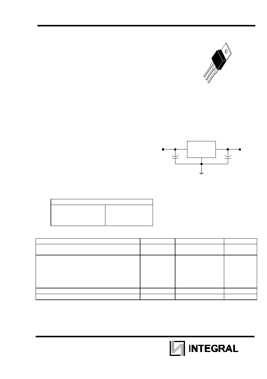
Pin 1. I nput
2. Ground
3. Output
(H eatsink
surface connected
to Pin 2.)
TO-220 AB
STANDARD APPLICATION
IL79XX
Co
1.0 F
Cin
0.33 F
input
output
A common ground is required between the input and
the output voltages. The input voltage must remain
typically 2.0V more negative even during the high
point on the input ripple voltage.
XX - these two digits of the type number indicate
voltage
Cin - is required if regulator is located an appreciable
distance from power supply filter
Co - improves stability and transient response

IL79XXC
SERIES
2
IL7905
Electrical characteristics
(V
I
= -10V, Io = 500mA, 0
úC <T
J
<+125
úC unless otherwise noted)
Characteristic
Symbol
Min Typ Max Unit
Output Voltage (TJ=+25
úC)
Vo -4.8 -5.0 -5.2 Vdc
Line Regulation (Note 1)
(TJ=+25
úC, Io = 100mA)
-7.0Vdc
ô V
I
ô -25Vdc
-8.0Vdc
ô V
I
ô -12Vdc
(TJ=+25
úC, Io =500mA)
-7.0Vdc
ô V
I
ô -25Vdc
-8.0Vdc
ô V
I
ô -12Vdc
Regline
-
-
-
-
7.0
2.0
35
8.0
50
25
100
50
mV
Load Regulation (TJ=+25
úC, Note 1)
5.0mA
ò Io ò 1.5A
250mA
ò Io ò 750 mA
Regload
-
-
11
4.0
100
50
mV
Output Voltage
5.0mA
ò Io ò 1.0A, Po ò15 W
-7.0Vdc
ô V
I
ô -25Vdc
Vo -4.75 - -5.25 Vcd
Input Bias Current (TJ=+25
úC)
I
IB
- 4.3
8.0
mA
Input Bias Current Change
-7.0Vdc
ô V
I
ô -25Vdc
5.0mA
ò Io ò 1.0A
I
IB
-
-
-
-
1.3
0.5
mA
Output Noise Voltage (TA=+25
úC)
10 Hz
ò f ò 100 kHz
e
on
- 40 -
V
Ripple Rejection (Io=20mA f=120Hz)
RR
-
70
-
dB
Dropout Voltage (Io=1.0A, T
J
=+25
úC)
V
I
-Vo - 2.0 - Vdc
Average Temperature Coefficient of
Output Voltage Io=5.0mA, 0
úC <T
J
<+125
úC
DVo/DT - -1.0 - mV/
úC
IL7905.2
Electrical characteristics
(V
I
= -10V, Io = 500mA, 0
úC <T
J
<+125
úC unless otherwise noted)
Characteristic
Symbol
Min Typ Max Unit
Output Voltage (TJ=+25
úC)
Vo -5.0 -5.2 -5.4 Vdc
Line Regulation (Note 1)
(TJ=+25
úC, Io = 100mA)
-7.2Vdc
ô V
I
ô -25Vdc
-8.0Vdc
ô V
I
ô -12Vdc
(TJ=+25
úC, Io =500mA)
-7.2Vdc
ô V
I
ô -25Vdc
-8.0Vdc
ô V
I
ô -12Vdc
Regline
-
-
-
-
8.0
2.2
37
8.5
52
27
105
52
mV
Load Regulation (TJ=+25
úC, Note 1)
5.0mA
ò Io ò 1.5A
250mA
ò Io ò 750 mA
Regload
-
-
12
4.5
105
52
mV
Output Voltage
5.0mA
ò Io ò 1.0A, Po ò15 W
-7.2Vdc
ô V
I
ô -20Vdc
Vo -4.95 - -5.45 Vcd
Input Bias Current (TJ=+25
úC)
I
IB
- 4.3
8.0
mA
Input Bias Current Change
-7.2Vdc
ô V
I
ô -25Vdc
5.0mA
ò Io ò 1.5A
I
IB
-
-
-
-
1.3
0.5
mA
Output Noise Voltage (TA=+25
úC)
10 Hz
ò f ò 100 kHz
e
on
- 42 -
V
Ripple Rejection (Io=20mA f=120Hz)
RR
-
68
-
dB
Dropout Voltage (Io=1.0A, T
J
=+25
úC)
V
I
-Vo - 2.0 - Vdc
Average Temperature Coefficient of
Output Voltage Io=5.0mA, 0
úC <T
J
<+125
úC
DVo/Vo - -1.0 - mV/
úC
Note:
1. Load and line regulation are specified at constant junction temperature. Changes in Vo due to heating effects must be taken into
account separately .Pulse testing with low duty cycle is used.
IL79XXC
SERIES
3
IL7906
Electrical characteristics
(V
I
= -11V, Io = 500mA, 0
úC <T
J
<+125
úC unless otherwise noted)
Characteristic
Symbol
Min Typ Max Unit
Output Voltage (TJ=+25
úC)
Vo -5.75 -6.0 -6.25 Vdc
Line Regulation (Note 1)
(TJ=+25
úC, Io = 100mA)
-8.0Vdc
ô V
I
ô -25Vdc
-9.0Vdc
ô V
I
ô -13Vdc
(TJ=+25
úC, Io =500mA)
-8.0Vdc
ô V
I
ô -25Vdc
-9.0Vdc
ô V
I
ô -13Vdc
Regline
-
-
-
-
9.0
3.0
43
10
60
30
120
60
mV
Load Regulation (TJ=+25
úC, Note 1)
5.0mA
ò Io ò 1.5A
250mA
ò Io ò 750 mA
Regload
-
-
13
5.0
120
60
mV
Output Voltage
5.0mA
ò Io ò 1.0A, Po ò15 W
-8.0Vdc
ô V
I
ô -21Vdc
Vo -5.7 - -6.3 Vcd
Input Bias Current (TJ=+25
úC)
I
IB
- 4.3
8.0
mA
Input Bias Current Change
-8.0Vdc
ô V
I
ô -25Vdc
5.0mA
ò Io ò 1.5A
I
IB
-
-
-
-
1.3
0.5
mA
Output Noise Voltage (TA=+25
úC)
10 Hz
ò f ò 100 kHz
e
on
- 45 -
V
Ripple Rejection (Io=20mA f=120Hz)
RR
-
65
-
dB
Dropout Voltage (Io=1.0A, T
J
=+25
úC)
V
I
-Vo - 2.0 - Vdc
Average Temperature Coefficient of
Output Voltage Io=5.0mA, 0
úC <T
J
<+125
úC
DVo/Vo - -1.0 - mV/
úC
IL7908
Electrical characteristics
(V
I
= -14V, Io = 500mA, 0
úC <T
J
<+125
úC unless otherwise noted)
Characteristic
Symbol
Min Typ Max Unit
Output Voltage (TJ=+25
úC)
Vo -7.7 -8.0 -8.3 Vdc
Line Regulation (Note 1)
(TJ=+25
úC, Io = 100mA)
-10.5Vdc
ô V
I
ô -25Vdc
-11Vdc
ô V
I
ô -17Vdc
(TJ=+25
úC, Io =500mA)
-10.5Vdc
ô V
I
ô -25Vdc
-11Vdc
ô V
I
ô -17Vdc
Regline
-
-
-
-
12
5.0
50
22
80
40
160
80
mV
Load Regulation (TJ=+25
úC, Note 1)
5.0mA
ò Io ò 1.5A
250mA
ò Io ò 750 mA
Regload
-
-
26
9.0
160
80
mV
Output Voltage
5.0mA
ò Io ò 1.0A, Po ò15 W
-10.5Vdc
ô V
I
ô -23Vdc
Vo -7.6 - -8.4 Vcd
Input Bias Current (TJ=+25
úC)
I
IB
- 4.3
8.0
mA
Input Bias Current Change
-10.5Vdc
ô V
I
ô -25Vdc
5.0mA
ò Io ò 1.5A
I
IB
-
-
-
-
1.0
0.5
mA
Output Noise Voltage (TA=+25
úC)
10 Hz
ò f ò 100 kHz
e
on
- 52 -
V
Ripple Rejection (Io=20mA f=120Hz)
RR
-
62
-
dB
Dropout Voltage (Io=1.0A, T
J
=+25
úC)
V
I
-Vo - 2.0 - Vdc
Average Temperature Coefficient of
Output Voltage Io=5.0mA, 0
úC <T
J
<+125
úC
DVo/Vo - -1.0 - mV/
úC
Note:
1. Load and line regulation are specified at constant junction temperature. Changes in Vo due to heating effects must be taken into
account separately. Pulse testing with low duty cycle is used.

IL79XXC
SERIES
4
IL7915
Electrical characteristics
(V
I
= -23V, Io = 500mA, 0
úC <T
J
<+125
úC unless otherwise noted)
Characteristic
Symbol
Min Typ Max Unit
Output Voltage (TJ=+25
úC)
Vo -14.4 -15 -15.6 Vdc
Line Regulation (Note 1)
(TJ=+25
úC, Io = 100mA)
-17.5Vdc
ô V
I
ô -30Vdc
-20Vdc
ô V
I
ô -26Vdc
(TJ=+25
úC, Io =500mA)
-17.5Vdc
ô V
I
ô -30Vdc
-20Vdc
ô V
I
ô -26Vdc
Regline
-
-
-
-
14
6.0
57
27
150
75
300
150
mV
Load Regulation (TJ=+25
úC, Note 1)
5.0mA
ò Io ò 1.5A
250mA
ò Io ò 750 mA
Regload
-
-
68
25
300
150
mV
Output Voltage
5.0mA
ò Io ò 1.0A, Po ò15 W
-17.5Vdc
ô V
I
ô -30Vdc
Vo -14.25 - -15.75 Vcd
Input Bias Current (T
J
=+25
úC)
I
IB
- 4.4
8.0
mA
Input Bias Current Change
-17.5Vdc
ô V
I
ô -30Vdc
5.0mA
ò Io ò 1.0A
I
IB
-
-
-
-
1.0
0.5
mA
Output Noise Voltage (TA=+25
úC)
10 Hz
ò f ò 100 kHz
e
on
- 90 -
V
Ripple Rejection (Io=20mA f=120Hz)
RR
-
60
-
dB
Dropout Voltage (Io=1.0A, T
J
=+25
úC)
V
I
-Vo - 2.0 - Vdc
Average Temperature Coefficient of
Output Voltage Io=5.0mA, 0
úC <T
J
<+125
úC
DVo/Vo - -1.0 - mV/
úC
IL7912
Electrical characteristics
(V
I
= -19V, Io = 500mA, 0
úC <T
J
<+125
úC unless otherwise noted)
Characteristic
Symbol
Min Typ Max Unit
Output Voltage (TJ=+25
úC)
Vo -11.5 -12 -12.5 Vdc
Line Regulation (Note 1)
(TJ=+25
úC, Io = 100mA)
-14.5Vdc
ô V
I
ô -30Vdc
-16Vdc
ô V
I
ô -22Vdc
(TJ=+25
úC, Io =500mA)
-14.5Vdc
ô V
I
ô -30Vdc
-16Vdc
ô V
I
ô -22Vdc
Regline
-
-
-
-
13
6.0
55
24
120
60
240
120
mV
Load Regulation (TJ=+25
úC, Note 1)
5.0mA
ò Io ò 1.5A
250mA
ò Io ò 750 mA
Regload
-
-
46
17
240
120
mV
Output Voltage
5.0mA
ò Io ò 1.0A, Po ò15 W
-14.5Vdc
ô V
I
ô -27Vdc
Vo -11.4 - -12.6 Vcd
Input Bias Current (T
J
=+25
úC)
I
IB
- 4.4
8.0
mA
Input Bias Current Change
-14.5Vdc
ô V
I
ô -30Vdc
5.0mA
ò Io ò 1.5A
I
IB
-
-
-
-
1.0
0.5
mA
Output Noise Voltage (TA=+25
úC)
10 Hz
ò f ò 100 kHz
e
on
- 75 -
V
Ripple Rejection (Io=20mA f=120Hz)
RR
-
61
-
dB
Dropout Voltage (Io=1.0A, T
J
=+25
úC)
V
I
-Vo - 2.0 - Vdc
Average Temperature Coefficient of
Output Voltage Io=5.0mA, 0
úC <T
J
<+125
úC
DVo/Vo - -1.0 - mV/
úC
Note:
1. Load and line regulation are specified at constant junction temperature. Changes in Vo due to heating effects must be taken into
account separately.Pulse testing with low duty cycle is used.
IL79XXC
SERIES
5
IL7918
Electrical characteristics
(V
I
= -27V, Io = 500mA, 0
úC <T
J
<+125
úC unless otherwise noted)
Characteristic
Symbol
Min Typ Max Unit
Output Voltage (TJ=+25
úC)
Vo -11.5 -12 -12.5 Vdc
Line Regulation (Note 1)
(TJ=+25
úC, Io = 100mA)
-21Vdc
ô V
I
ô -33Vdc
-24Vdc
ô V
I
ô -30Vdc
(TJ=+25
úC, Io =500mA)
-21Vdc
ô V
I
ô -33Vdc
-24Vdc
ô V
I
ô -30Vdc
Regline
-
-
-
-
25
10
90
50
180
90
360
180
mV
Load Regulation (TJ=+25
úC, Note 1)
5.0mA
ò Io ò 1.5A
250mA
ò Io ò 750 mA
Regload
-
-
110
55
360
180
mV
Output Voltage
5.0mA
ò Io ò 1.0A, Po ò15 W
-21Vdc
ô V
I
ô -33Vdc
Vo -17.1 - -18.9 Vcd
Input Bias Current (T
J
=+25
úC)
I
IB
- 4.5
8.0
mA
Input Bias Current Change
-21Vdc
ô V
I
ô -33Vdc
5.0mA
ò Io ò 1.5A
I
IB
-
-
-
-
1.0
0.5
mA
Output Noise Voltage (TA=+25
úC)
10 Hz
ò f ò 100 kHz
e
on
- 110 -
V
Ripple Rejection (Io=20mA f=120Hz)
RR
-
59
-
dB
Dropout Voltage (Io=1.0A, T
J
=+25
úC)
V
I
-Vo - 2.0 - Vdc
Average Temperature Coefficient of
Output Voltage Io=5.0mA, 0
úC <T
J
<+125
úC
DVo/Vo - -1.0 - mV/
úC
IL7924
Electrical characteristics
(V
I
= -33V, Io = 500mA, 0
úC <T
J
<+125
úC unless otherwise noted)
Characteristic
Symbol
Min Typ Max Unit
Output Voltage (TJ=+25
úC)
Vo -11.5 -12 -12.5 Vdc
Line Regulation (Note 1)
(TJ=+25
úC, Io = 100mA)
-27Vdc
ô V
I
ô -38Vdc
-30Vdc
ô V
I
ô -36Vdc
(TJ=+25
úC, Io =500mA)
-27Vdc
ô V
I
ô -38Vdc
-30Vdc
ô V
I
ô -36Vdc
Regline
-
-
-
-
31
14
118
70
240
120
480
240
mV
Load Regulation (TJ=+25
úC, Note 1)
5.0mA
ò Io ò 1.5A
250mA
ò Io ò 750 mA
Regload
-
-
150
85
480
240
mV
Output Voltage
5.0mA
ò Io ò 1.0A, Po ò15 W
-27Vdc
ô V
I
ô -38Vdc
Vo -22.8 - -25.2 Vcd
Input Bias Current (T
J
=+25
úC)
I
IB
- 4.6
8.0
mA
Input Bias Current Change
-27Vdc
ô V
I
ô -38Vdc
5.0mA
ò Io ò 1.5A
I
IB
-
-
-
-
1.0
0.5
mA
Output Noise Voltage (TA=+25
úC)
10 Hz
ò f ò 100 kHz
e
on
- 170 -
V
Ripple Rejection (Io=20mA f=120Hz)
RR
-
56
-
dB
Dropout Voltage (Io=1.0A, T
J
=+25
úC)
V
I
-Vo - 2.0 - Vdc
Average Temperature Coefficient of
Output Voltage Io=5.0mA, 0
úC <T
J
<+125
úC
DVo/Vo - -1.0 - mV/
úC
Note:
Load and line regulation are specified at constant junction temperature. Changes in Vo due to heating effects must be taken into
account separately. Pulse testing with low duty cycle is used.