 | –≠–ª–µ–∫—Ç—Ä–æ–Ω–Ω—ã–π –∫–æ–º–ø–æ–Ω–µ–Ω—Ç: ILA6107Q | –°–∫–∞—á–∞—Ç—å:  PDF PDF  ZIP ZIP |
ILA6107Q
1
Triple video output amplifier
GENERAL DESCRIPTION
The ILA6107Q includes three video output amplifiers in one plastic DIL-bent-SIL 9-pin medium power
(DBS9MPF) package (SOT111-1), using high-voltage DMOS technology, and is intended to drive the three
cathodes of a colour CRT directly. To obtain maximum performance, the amplifier should be used with black-
current control
FEATURES
û Typical bandwidth of 5.5 MHz for an output signal of 60 V (p-p)
û High slew rate of 900 V/s
û No external components required
û Very simple application
û Single supply voltage of 200 V
û Internal reference voltage of 2.5 V
û Fixed gain of 50
û Black-Current Stabilization (BCS) circuit
û Thermal protection.
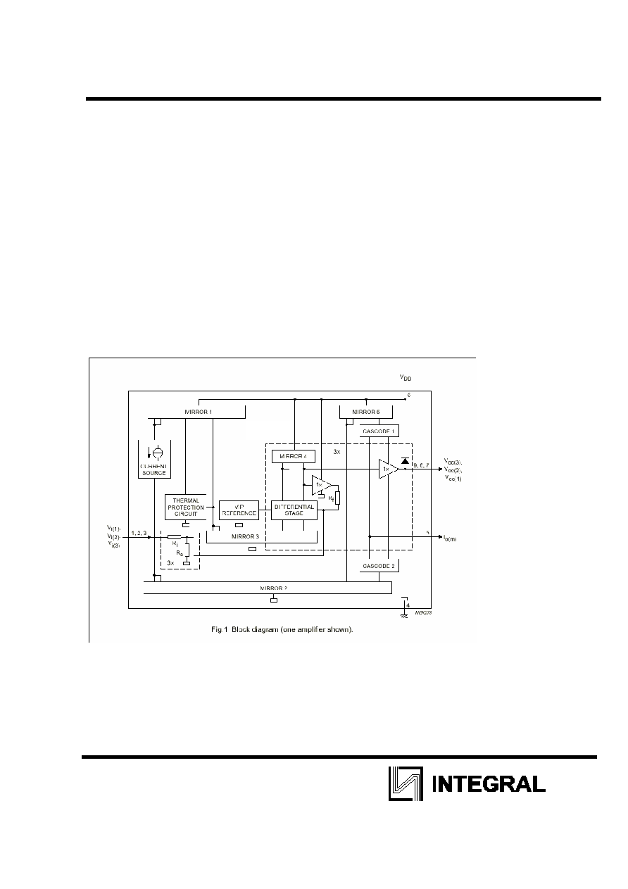
BLOCK DIAGRAM
ILA6107Q

ILA6107Q
2
PINNING
SIMBOL PIN
DESCRIPTION
V
i(1)
1
inverting
input
1
V
i(2)
2
inverting
input
2
V
i(3)
3
inverting
input
3
GND 4
ground
(fin)
I
om
5
black-current
measurement
output
V
DD
6
supply
voltage
V
oc(3)
7
cathode
output
3
V
oc(2)
8
cathode
output
2
V
oc(1)
9
cathode
output
1
V
1
I(1)
V
2
I(2)
V
3
I(2)
GND 4
I 5
O M
V 6
DD
V
7
CC(3)
V
8
CC(2)
V
9
CC(1)
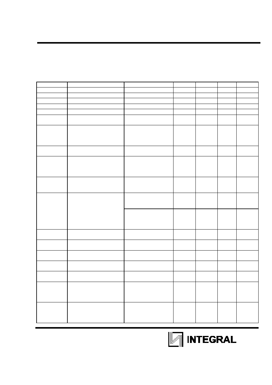
LIMITING VALUES
In accordance with the Absolute Maximum Rating System (IEC 134); voltage measured with respect to pin 4
(ground); currents as specified in Fig. 1; unless otherwise specified.
SYMBOL PARAMETER
MIN.
MAX.
UNIT
V
DD
supply
voltage
0
250
V
i
supply voltage at pins 1 to 3
0
12
V
o(m)
measurement output voltage
0
6
V
o(c)
cathode output voltage
0
V
DD
T
stg
storage
temperature
-55
+150
úC
T
j
junction
temperature
-20
+150
úC
V
es
electrostatic
handling
Human Body Model (HBM)
Machine Model (MM)
-
-
2000
300
V
V
HANDLING
Inputs and outputs are protected against electrostatic discharge in normal handling. However, to be totally safe,
it is desirable to take normal precautions appropriate to handling MOS devices (see "Handling MOS Devices").
QUALITY SPECIFICATION
Quality specification "SNW-FQ-611 part D " is applicable and can be found in the "Quality reference Handbook ".
The handbook can be ordered using the code (9397 750 00192.

ILA6107Q
3
THERMAL HARACTERISTICS
SYMBOL PARAMETER CONDITIONS
VALUE
UNIT
R
th(j-a)
thermal resistance from junction to ambient
56
K/W
R
th(j-fin)
thermal resistance from junction to fin
note 1
11
K/W
R
th(h-a)
thermal resistance from heatsink to ambient
18
K/W
Note
1. An external heatsink is necessary.
ILA6107Q
4
CHARACTERISTICS
Operating range: T
j
= -20 to +150
úC; V
DD
= 180 to 210 V. Test conditions: T
amb
= 25
úC; V
DD
= 200 V ;
V
o(c1)
= V
o(c2)
= V
o(c3)
= V
DD
; C
L
= 10 pF (C
L
consists of parasitic and cathode capacitance); R
th(h-a)
= 18 K/W;
unless otherwise specified.
SYMBOL PARAMETER CONDITIONS
MIN.
TYP.
MAX.
UNIT
I
q
quiescent
supply
current
5.9
6.9
7.9
mA
V
ref(int)
internal reference voltage
-
2.5
-
V
R
j
input
resistance
-
3.6
-
k
G amplifier
47.5
51.0
55.0
G
gain difference
-2.5
0
+2.5
V
o(c)
nominal output voltage at
pins 7, 8 and 9 (DC value)
I
i
= 0
A
116 129 142
V
V
o(c)(offset)
differential nominal output
offset voltage between pins
7 and 8, 8 and 9 and 9 and
7 (DC value)
I
i
= 0
A
- 0 5
V
V
o(c)(T)
output voltage temperature
drift at pins 7, 8 and 9
-
-10
-
mV/K
V
o(c)(T)(offset)
differential output offset
voltage temperature drift
between pins 7 and 8, 8
and 9 and 7 and 9
-
0
-
mV/K
I
o(m)(offset)
offset
current
of
measurement output
I
o(c)
= 0
A
1.5 V < V
i
<5.5 V
3 V < V
o(m)
< 6 V
-50 -
+50
A
-100
A < I
o(c)
< 100
A
1.5 V < V
i
<5.5 V
3 V < V
o(m)
< 6 V
0.9 1.0 1.1
I
o(m)
/
I
o(c)
linearity of current transfer
at CRT discharge;
I
o(c)
= 1 mA
1.5 V < V
i
<5.5 V
3 V < V
o(m)
< 5.4 V
- 1.0
-
I
o(c)(max)
maximum peak output
current (pins 7, 8 and 9)
50 V < V
o(c)
< V
DD
- 50
V
- 20
-
mA
V
o(c)(min)
minimum output voltage
(pins 7, 8 and 9)
V
i
= 7.0 V
-
-
10
V
V
o(c)(max)
maximum output voltage
(pins 7, 8 and 9)
V
i
= 1.0 V
V
DD
- 15 -
-
V
B
S
small signal bandwidth
(pins 7, 8 and 9)
V
o(c)
= 60 V (p-p)
-
5.5
-
MHz
B
L
large signal bandwidth
(pins 7, 8 and 9)
V
o(c)
= 100 V (p-p)
-
4.5
-
MHz
t
Pco
cathode output propagation
time 50% input to 50%
output (pins 7, 8 and 9)
V
o(c)
= 100 V (p-p)
square wave; f < 1
MHz; t
r
= t
f
= 40 ns
(pins 1, 2 and 3);
- 60
-
ns
t
Pco
difference in cathode
output propagation time
50% input to 50% output
(pins 7and 8, 7 and 9 and 8
V
o(c)
= 100 V (p-p)
square wave; f < 1
MHz; t
r
= t
f
= 40 ns
(pins 1, 2 and 3);
- 10
0
+ 10
ns

ILA6107Q
5
SYMBOL PARAMETER CONDITIONS
MIN.
TYP.
MAX.
UNIT
and 9)
t
o(r)
cathode output rise time
10% output to 90% output
(pins 7, 8 and 9)
V
o(c)
= 50 to 150 V
square wave; f < 1
MHz; t
f
= 40 ns
(pins 1, 2 and 3);
67 91 113
ns
t
o(f)
cathode output fall time
90% output to 10% output
(pins 7, 8 and 9)
V
o(c)
= 50 to 150 V
square wave; f < 1
MHz; t
f
= 40 ns
(pins 1, 2 and 3);
67 91 113
ns
t
st
Setting time 50% input to
99% < output < 101% (pins
7, 8 and 9)
V
o(c)
= 100 V (p-p)
square wave; f < 1
MHz; t
r
= t
f
= 40 ns
(pins 1, 2 and 3);
- - 350
ns
SR
slew rate between 50 V to
(V
DD
- 50 V) (pins 7, 8 and
9)
V
i
= 4 V (p-p) square
wave;
f < 1 MHz; t
r
= t
f
= 40
ns
(pins 1, 2 and 3);
- 900
-
V/
s
O
v
cathode output voltage
overshoot (pins 7, 8 and 9)
V
i
= 100 V (p-p) square
wave;
f < 1 MHz; t
r
= t
f
= 40
ns
(pins 1, 2 and 3);
- 2 -
%
PSRR
Power supply rejection
ratio
f < 50 kHz; note 1
-
55
-
dB
ct(DC)
DC crosstalk between
channels
-
50
-
dB
Notes
1. The ratio of the change in supply voltage to the change in input voltage when there is no change in output
voltage.