 | –≠–ª–µ–∫—Ç—Ä–æ–Ω–Ω—ã–π –∫–æ–º–ø–æ–Ω–µ–Ω—Ç: ILA8395N | –°–∫–∞—á–∞—Ç—å:  PDF PDF  ZIP ZIP |

TECHNICAL DATA
ILA8395N
SECAM decoder
FEATURES
ûFully integrated filters
ORDERING INFORMATION
ILA8395N
DIP
T
A
= -40
ú to 125úC
1
8
16
ûAlignment free
ûFor use with baseband delay
GENERAL DESCRIPTION
The ILA8395N is a self-calibrating, fully integrated SECAM
decoder. The IC should preferably be used in conjunction with the
PAL/NTSC decoder ILA8362ANS (TDA8362A) or TDA8366 and with
the switched capacitor baseband delay circuit ILA4661 (TDA4661,
TDA4660). The IC incorporates HF and LF filters, a demodulator and an
identification circuit (luminance is not processed in this IC). The IC needs
no adjustments and very few external components are required. A highly
stable reference frequency is required for calibration and a two-level
sandcastle pulse for blanking and burst gating.
QUICK REFERENCE DATA
SYMBOL PARAMETER MIN.
MAX.
UNIT
V
p
Positive supply voitage; pin 3
7.2
8.8
V
V
16(p-p)
Composite video input voltage
(peak -to- peak value); pin 16
- 1.5
V
T
stg
Storage temperature range
-25
+150
úC
T
amb
Operation ambient temperature range
-25
+70
úC
1
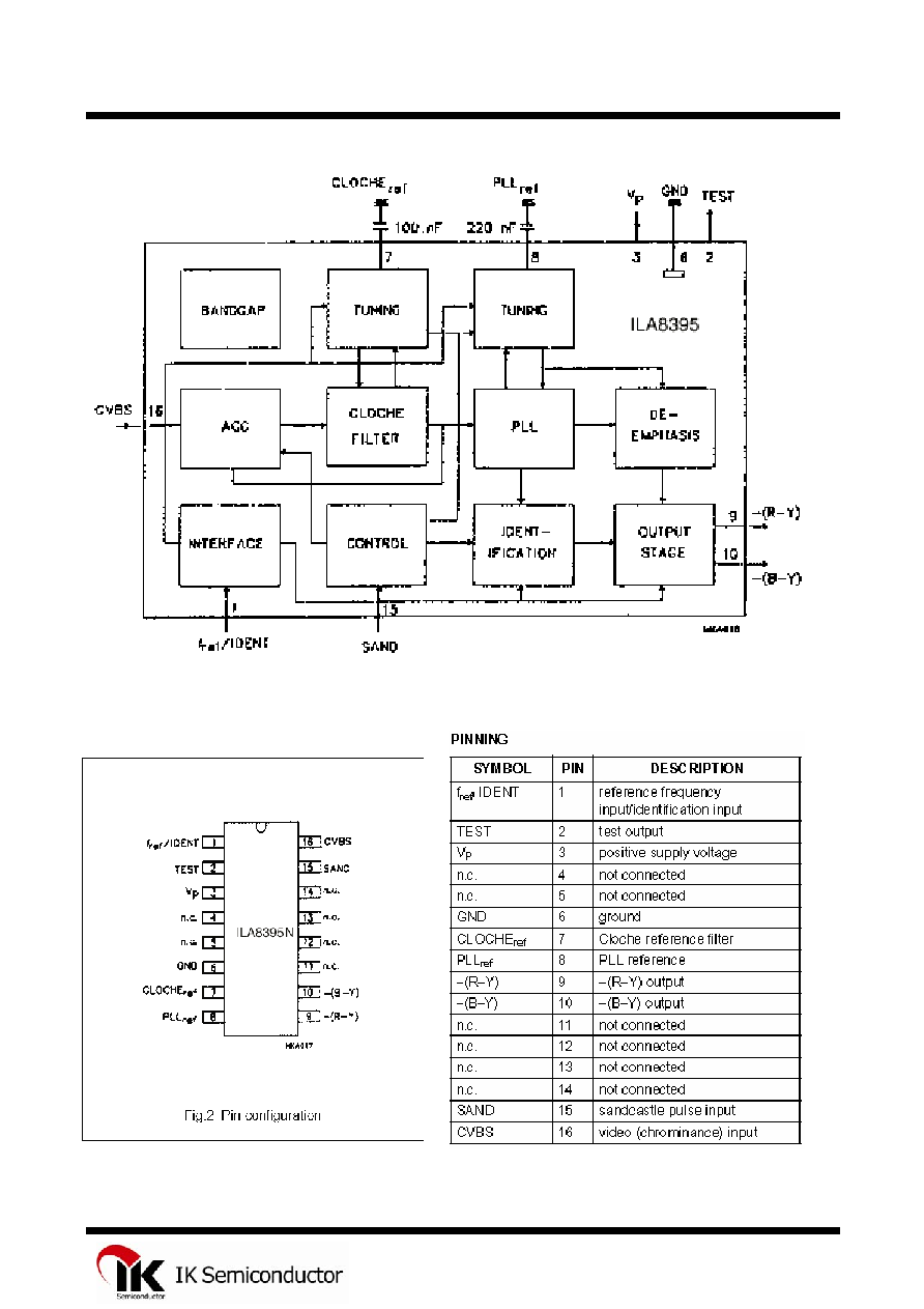
ILA8395N
Fig.1 Block diagram.
2

ILA8395N
FUNCTIONAL DESCRIPTION
The ILA8395N is a self-calibrating SECAM decoder designed for use with a baseband delay circuit. During
frame retrace a 4.433619 MHz reference frequency is used to calibrate the filters and the demodulator. The reference
frequency should be very stable during this period.
The Cloche filter is a gyrator-capacitor type filter the resonance frequency of which is controlled during the
calibration period and offset during scan; this ensures the correct frequency during calibration. The demodulator is a
Phase-Locked Loop (PLL) type demodulator which uses the frequency reference and the bandgap reference to force the
PLL to the required demodulation characteristic.
The low frequency de-emphasis is matched to the PLL and is controlled by the tuning voltage of the PLL. A
digital identification circuit scans the incoming signal for SECAM (only line-identification is implemented). The
identification circuit needs to communicate with the ILA8362ANS to guarantee that the output signal from the decoder
is only available when no PAL signal has been identified. If a SECAM signal is decoded a request for colour-on is
transmitted to pin 1 (current is sunk). If the signal request is granted (i.e. pin 1 is HIGH therefore no PAL) the colour
difference outputs ((BY) and (RY)) from the ILA8362 are high impedance and the output signals from the ILA8395N
are switched ON.
If no SECAM signal is decoded during a two-frame period the demodulator will be initialized before another
attempt is made also during a two-frame period. The CD outputs will be blanked or high-impedance depending on the
logic level at pin 1.
A two-level sandcastle pulse generates the required blanking periods and, also, clocks the digital identification
pulse on the falling edge of the burst gate pulse. To enable the calibration period to be defined the vertical retrace is
discriminated from the horizontal retrace, this is achieved by measuring the width of the blanking period.
APPLICATION INFORMATION
The leakage current at pin 8 should be well below 20 nA to meet the specification of the black levels (C8 = 220
nF).
The leakage current at pin 7 should be well below 60 nA to meet the specification of the Cloche resonance
frequency (C7 = 100 nF).
The capacitors C7 and C8 should be connected to the ground pin as close as possible to the package. If not, this
can result in a black level error for both channels.
TEST INFORMATION
The performance of the Cloche filter can be measured at pin 2. The use of a FET-probe is advised for low
capacitive loading.
3

ILA8395N
CHARACTERISTICS
VP = 8.0 V; Tamb = 25 úC; unless otherwise specified
SYMBOL PARAMETER
CONDITIONS
MIN.
TYP.
MAX.
UNIT
Supply (pin 3)
V
p
positive supply voltage
7.2
8.0
8.8
V
I
p
supply current
18
25
mA
P
tot
Total power dissipation
-
144
220
mV
CVBS input (pin 10)
V
16(p-p)
composite video input voltage
(peak to peak value)
- 1.0
1.5
V
V
16(p-p)
chrominance video input
voltage (peak to peak value)
Note 1
15
-
300
mV
Z
1
Input impedance
Note 2
-
15
-
k
CLOCHE (pin 7)
V
td
tuning voltage; pin 7
2.5
3.5
4.5
V
f
0
resonance frequency
Note 3
4.266
4.286
4.306
MHz
B bandwidth
241
268
295
kHz
Demodulator
V
td
tuning voltage; pin 8
3.5
-
4.8
V
V
0(p-p)
100/75 color bar
0.97
1.05
1.13
V
V
0(p-p)
100/75 color bar
1.23
1.33
1.43
V
NLE non-lineanty
error
100/75 color bar
note 4
- - 3
%
-(B-Y) /(R-Y)
ratio of -(B-Y) and -(R-Y)
1.23
1.27
1.32
F
be
-(R-Y)
black level error - (R-Y)
Note 5
-
-
5
kHz
F
be
-(B-Y)
black level error - (B-Y)
Note 5
-
-
7
kHz
V
o
Output voltage levelduring
blanking
- 2.8
-
V
B
o
Output bankwidth
-
1.3
-
MHz
S/N
signal-to-noise ratio
Note 6
40
-
-
dB
f
p
pole-frequency LF de-
emphasis
77
85
93
kHz
f
p
/f
o
ratio of pole and zero frequency
-
3
-
V
rh(p-p)
residual harmonic voltage
(peak to peak value)
- - 10
mV
Z
o(e)
output impedance SECAM
enabled
Pin 1 HIGH
-
-
600
Z
o(d)
output impedance SECAM
disabled
Pin 1 LOW
1
-
-
M
Sandcastle pulse
V
bl
blanking detection level
1.0
1.25
1.5
V
V
b0
burst gate detection level
3.5
3.85
4.2
V
t
f
falling edge of burst gate to
start syne
8.5
9.0
9.5
s
Reference/communication
f
ref
reference frequency
Note 7
-
4.4336
-
MHz
V
ref(p-p)
reference voltage amplitude
(peak to peak value)
0.20
- 0.50
V
4

ILA8395N
SYMBOL PARAMETER
CONDITIONS
MIN.
TYP. MAX. UNIT
V
ed
SECAM enable detection
level; pin 1
- 2.8
3.3
V
V
dd
SECAM disabled detection
level; pin 1
Note 8
1.5
2.0
-
V
I
s
sink current at SECAM
identification; pin 1
Note 9
-
150
-
A
Identification
t
i
Identification time
-
4
-
frames
H
colour on/off hysteresis
3
-
-
dB
Notes to the characteristics
1.If measured in the burst-period of a blue line.
2.The video input is AC-coupled.
3.During scan.
4. Measured as 100% x (IVuI - IVII) / (IVuI + IVlI); see Fig.3.
5. Converted to input frequency error.
6. Defined as the ratio between the peak-to-peak value of the B-Y component of the demodulated 100/75 colour bar
and the peak-to-peak value of the noise.
7. The reference should be stable during frame blanking.
8. The SECAM enable and disable timing should preferably be at the end of the frame blanking.
9. The externally supplied voltage should exceed 0.5 V.
5