 | –≠–ª–µ–∫—Ç—Ä–æ–Ω–Ω—ã–π –∫–æ–º–ø–æ–Ω–µ–Ω—Ç: ILE4267 | –°–∫–∞—á–∞—Ç—å:  PDF PDF  ZIP ZIP |
ILE4267
1
5-V Low-Drop Voltage Regulator
Functional Description
ILE 4267 is a 5-V low-drop voltage regulator. It
supplies an output current of > 400 mA. The IC is
shortcircuit-proof and incorporates temperature
protection that disables the 1C at overtemperature
Features
û Output voltage tolerance ò 2 %
û 400 mA output current capability
û Low-drop voltage
û Very low standby current consumption
û Input voltage up to 40 V
û Overvoltage protection up to 60 V (ò 400 ms)
û Reset function down to 1 V output voltage
û ESD protection up to 2000 V
û Adjustable reset time
û On/off logic
û Overtemperature protection
û Reverse polarity protection
û Short-circuit proof
û Wide temperature range
û
Suitable for use in automotive electronics
Application
The IC regulates an input voltage V, in the range 5.5 V < Vi < 40 V to V
Qrated
= 5.0 V. A
reset signal is generated for an output voltage V
Q
of < 4.5 V. The reset delay can be set
with an external capacitor. The device has two logic inputs. It is turned-ON by a voltage of
> 4 V on E2 by the ignition for example. It remains active as a function of the voltage on
E6, even if the voltage on E2 goes Low. This makes it possible to implement a self-holding
circuit without external components. When the device is turned-OFF, the output voltage
drops to 0 V and current consumption tends towards 0
A
.
Design Notes for External Components
The input capacitor Ci
is necessary for compensation line influences. The resonant circuit
consisting of lead inductance and input capacitance can be damped by a resistor of approx. 1
in
series with Ci. The output capacitor is necessary for the stability of the regulating circuit. Stability is
guaranteed at values of
ô 22 F and an ESR of ò 3 within the operating temperature range.
Circuit Description
The control amplifier compares a reference voltage, which is kept highly accurate by resistance
adjustment, to a voltage that is proportional to the output voltage and drives the base of

ILE4267
2
the series transistor via a buffer. Saturation control as a function of the load current
prevents any over-saturating of the power element.
A comparator in the reset-generator block compares a reference that is independent of the
input voltage to the scaled-down output voltage. If this reaches a value of 4.5 V, the reset-
delay capacitor is discharged and then the reset output is set Low. As the output voltage
increases again, the reset-delay capacitor is charged with constant current from V
Q
= 4.5
V onwards. When the capacitor voltage reaches the upper switching threshold, reset goes
High again. The reset delay can be set within wide range by selection of the external
capacitor.
With the integrated tum-ON/tum-OFF logic it is simple to implement delayed tum-OFF
without external components.
Truth Table for Turn-ON/Turn-OFF Logic
E2, Inhibit
Hold
V
Q
Remarks
L
X
OFF
Initial state. Inhibit internally pulled up
H
X
ON
Regulator switched on via Inhibit, by ignition for example
H
L
ON
Hold clamped active to ground by controller while Inhibit is still high
X
L
ON
Previous state remains, even ignition is shut off: self-holding state
L
L
ON
Ignition shut off while regulator is in self-holding state
L
H
OFF
Regulator shut down by releasing of Hold while Inhibit remains Low,
final state. No active clamping required by external self-holding
circuit (
C) to keep regulator shut off.
Inhibit: E2 Enable function, active High
Hold: E6 Hold and release function, active Low
ILE4267
3
Pin Definitions and Functions
Pin Symbol
Function
1 I
Input; block to ground directly at the IC by a ceramic capacitor
2 E2 Inhibit; device is turned-ON by High signal on this pin; internal pulldown
resistor of 100 k
3 R Reset Output; open-collector output internally connected to the output
via a resistor of 30 k
4 GND
Ground; connected to rear of chip
5 D Reset Delay; connect with capacitor to GND for setting delay
6 E6 Hold; see truth table above for function; this input is connected to output
voltage across puliup resistor of 50 k
7 Q 5-V Output; block to GND with 22-
F capacitor, ESR < 3
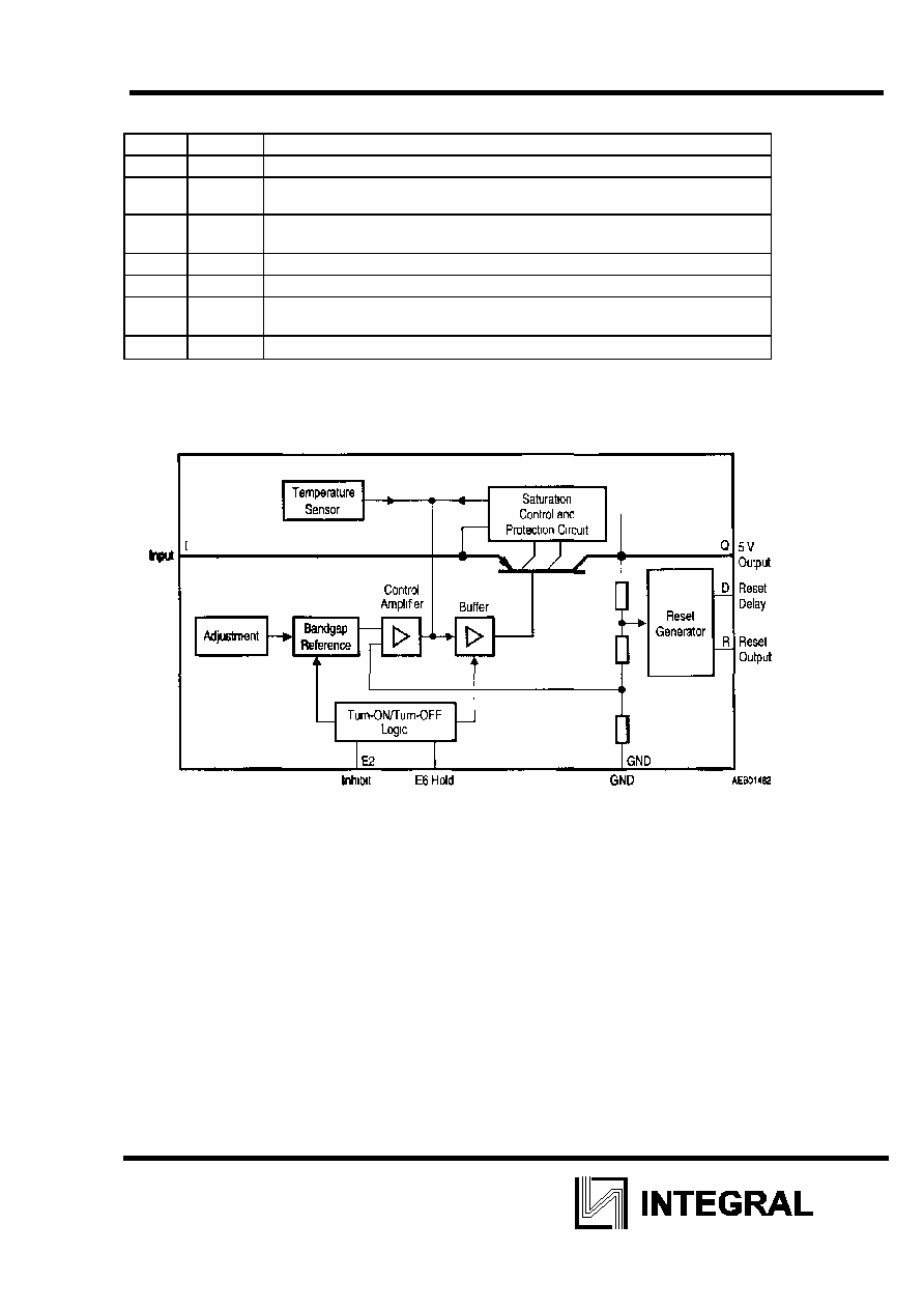
Block Diagram

ILE4267
4
Absolute Maximum Ratings
T
J
= -40 to 150úC
Limit Values
Parameter
Symbol
min. max.
Unit
Notes
Input
Voltage Vi
-42
42
V
-
Voltage Vi
-
60
V
t
ò 400 ms
Current Ii
-
-
-
Limited
internally
Reset Output
Voltage V
R
-0.3
7 V
-
Current I
R
- - -
Limited
internally
Reset Delay
Voltage Vd
-0.3
42
V
-
Current Id
-
-
-
-
Output
Voltage V
Q
-0.3
7 V
-
Current I
Q
- - -
Limited
internally
Inhibit
Voltage V
E2
-42
42 V
-
Current l
E2
-5 5 mA
t
ò 400 ms
Hold
Voltage V
E6
-0.3 7
V
-
Current I
E6
-
-
mA Limited
internally
GND
Current I
GND
-0.5 -
A
-
Temperatures
Junction temperature
T
J
-
150 úC -
Storage temperature
Tstg
-50
150
úC
-
Operating Range
Limit Values
Parameter
Symbol
min. max.
Unit
Notes
Input voltage
Vi
5.5
40
V
see diagram
Junction temperature
T
J
-40 150
úC
-
Thermal Resistance
Junction ambient
-
65
K/W
P-T0220-7-3 package
Junction-case Rthjc
-
6
K/W
P-T0220-7-3
package
Junction-case
Zthjc
-
2
K/W
T< 1 ms
P-T0220-7-3 package
Junction ambient
Rthja
-
70
K/W
P-T0220-7-180 (SMD) package
Junction-case
Rthjc
-
6
K/W
P-T0220-7-180 (SMD) package
Junction-case
Zthjc
-
2
K/W
T<1 ms
P-T0220-7-180 (SMD) package
Junction ambient
Rthja
-
65
K/W
P-T0220-7-230 package
Junction-case Rthjc
-
6
K/W
P-T0220-7-230
package
Junction-case
Zthjc
-
2
K/W
T< 1 ms
P-T0220-7-230 package
Junction ambient
Rthja
-
70
K/W
P-DSO-14-8 package
Junction-pin Rthjc
-
30
K/W
P-DSO-14-8
package
Characteristics
Vi = 13.5 V; - 40 úC < T
J
< 125 úC; V
E2
> 4 V (unless specified otherwise)
Parameter
Symbol
Limit Values
Unit
Test Condition

ILE4267
5
min. typ. max.
Output voltage
V
Q
4.9
5 5.1
V 5 mA
ò I
Q
ò 400 mA 6 V
ò Vi ò 26 V
Output voltage
V
Q
4.9
5 5.1
V 5mA
ò I
Q
ò 150 mA
6 V
ò Vi ò 40 V
Output-current limiting
I
Q
500 -
-
mA T
J
= 25 úC
Current consumption
Iq = Ii - I
Q
Iq --
--
50
A
Regulator-OFF
Current consumption
Iq = Ii - I
Q
Iq --
1.0
10
mA
T
J
= 25 úC
IC turned off
Current consumption
Iq = Ii - I
Q
Iq --
1.3
4
mA
I
Q
= 5 mA
IC turned on
Current consumption
Iq = Ii - I
Q
Iq
--
--
60
mA
I
Q
= 400 mA
Current consumption
Iq = Ii - I
Iq --
--
80
mA
I
Q
= 400 mA
V
I
= 5 V
Drop voltage
V
Dr
-
0.3
0.6
V I
Q
= 400 mA
1
'
Load regulation
V
Q
- -
50 mV 5 mA
ò. I
Q
ò 400 mA
Supply-voltage regulation V
Q
--
15
25
mV
Vi = 6 to 36 V;
I
Q
= 5 mA
Supply-voltage rejection
SVR
--
54
--
dB
Fr = 100Hz;
Vr = 0.5Vpp
Longterm stability
V
Q
- 0 - mV 1000
h
Reset Generator
Switching threshold
Vn
4.2
4.5
4.8
V
-
Reset High level
-
4.5
-
-
V
Rext =
Saturation voltage
V
R
-
0.1
0.4
V R
R
= 4.7 k
2
)
Pullup R
R
-
30
-
k
-
Saturation voltage
V
D
,sat. -
50
100 mV V
Q
< V
RT
Charge current
Id
8
15
25
A
V
D
= 1.5V
Delay switching threshold Vdt
2.6
3
3.3
V
-
Delay
td
-
20
-
ms
Cd = 100nF
Switching threshold
Vst
-
0.43
-
V
-
Delay
t
t
-
2
-
s
Cd = 100nF
Inhibit
Turn-ON voltage
V
E2
-
3 4
V IC
turned-ON
Turn-OFF voltage
V
E2
2
- - V IC
turned-OFF
Pulldown R
E2
50
100
200
k
-
Hysteresis
V
E2
0.2 0.5 0.8 V
-
Input current
I
E2
-
35
100
A
V
IP2
= 4 V
Holding voltage
V
E6
30
35
40
%
Referred to V
Q
Turn-OFF voltage
V
E6
60
70
80
%
Referred to V
Q
Pullup R
E6
20
50 100
k
-
Overvoltage Protection
Turn-OFF voltage
Vi, ov
42
44
46
V
-
Turn-ON hysteresis
Vi, ov
2 - 6 V -