 | –≠–ª–µ–∫—Ç—Ä–æ–Ω–Ω—ã–π –∫–æ–º–ø–æ–Ω–µ–Ω—Ç: IN1489AD | –°–∫–∞—á–∞—Ç—å:  PDF PDF  ZIP ZIP |
TECHNICAL DATA
1
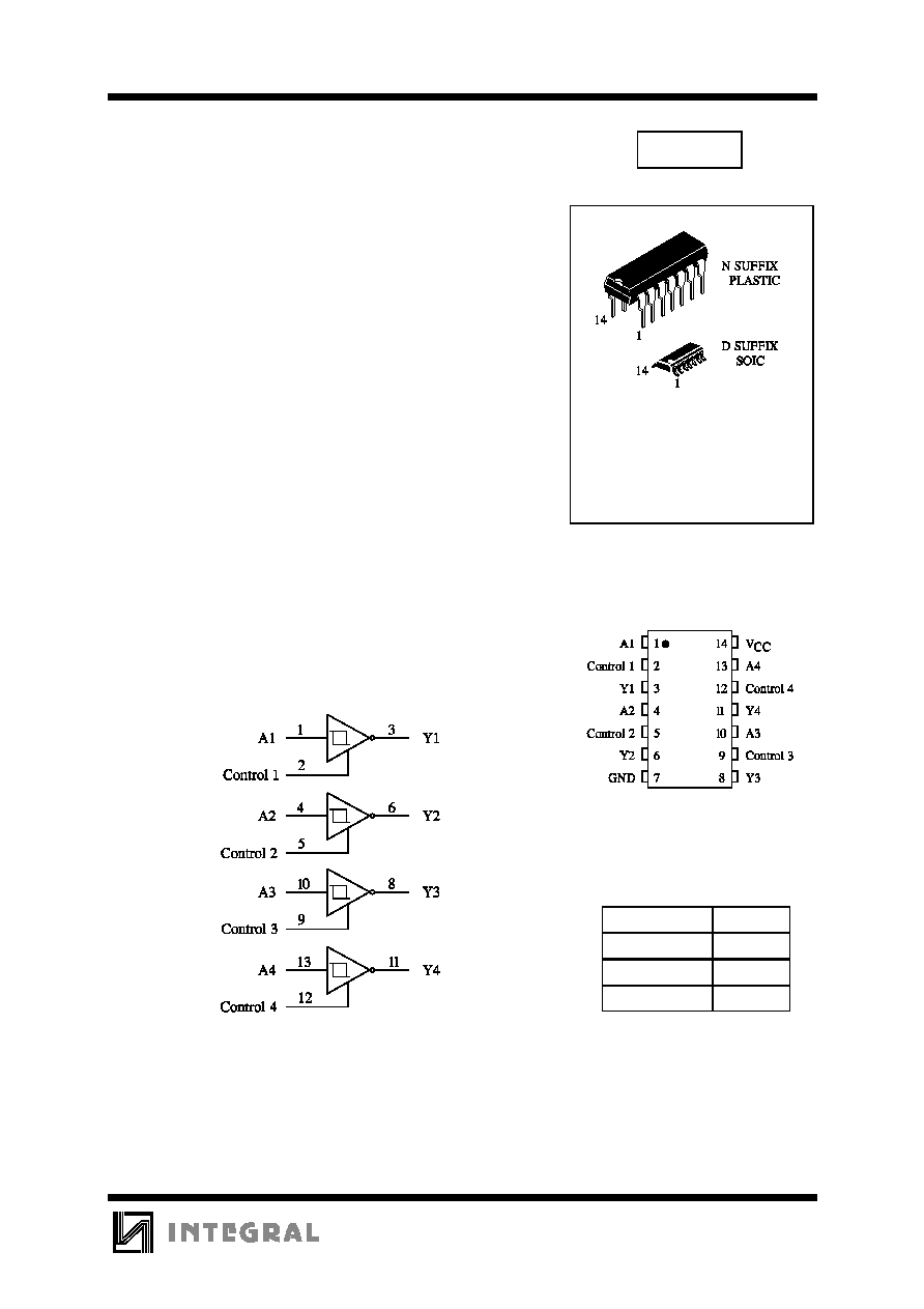
Qudruple Line Receivers
The IN1489A is a monolithic quadruple line receivers designed to
satisfy the requirements of the standard interface between data terminal
equipment and data communication equipments as defined by EIA
standard RS-232C. A separate response control terminal is provided
for each receiver. A resistor or a resistor and bias voltage can be
connected between this terminal and ground to shift the input threshold
voltage levels. An external capacitor can be connected from this
terminal to ground to provide input noise filtering.
û Input Resistance ... 3 k to 7k
û Input Signal Range ... 30 V
û Operates from Single 5 V Supply
û Built-IN Input Hysteresis (Double Thresholds)
û Response Control Provides: Input Tresold
Shifting
Input Noise Filtering
û Satisfies Requirements of EIA RS-232C
IN1489A
ORDERING INFORMATION
IN1489AN Plastic
IN1489AD SOIC
T
A
= -10
ú to 70ú C
for all packages
LOGIC DIAGRAM
PIN 14 =V
CC
PIN 7 = GND
PIN ASSIGNMENT
FUNCTION TABLE
Inputs
Output
A
Y
L
H
H
L

IN1489A
2
MAXIMUM RATINGS
*
Symbol
Parameter
Value
Unit
V
CC
Supply Voltage
6
V
V
IN
Input Voltage
25
V
I
O
Output Current
10
mA
Tstg
Storage Temperature Range
-65 to +150
úC
*
Maximum Ratings are those values beyond which damage to the device may occur.
Functional operation should be restricted to the Recommended Operating Conditions.
RECOMMENDED OPERATING CONDITIONS
Symbol
Parameter
Min
Max
Unit
V
CC
Supply Voltage
5.5
V
V
IH
High Level Input Voltage
25
V
V
IL
Low Level Input Voltage
-25
V
I
OL
Low Level Output Current
10
mA
T
A
Ambient Temperature Range
-10
+70
úC
DC ELECTRICAL CHARACTERISTICS over full operating conditions
Guaranteed Limit
Symbol
Parameter
Test Conditions
Min
Max
Unit
V
T+
Positive-Going Tthreshold
Input Voltage
1.75
2.25
V
V
T-
Negaitive-Going Tthreshold
Voltage
0.75
1.25
V
V
OH
High-Level Output Voltage
V
I
= 0.75 V, I
OL
= -0.5 mA
2.6
V
Input open, I
OH
=-0.5 mA
2.6
V
OL
High-Level Output Voltage
V
I
= 3 V, I
OL
= 10 mA
0.45
V
I
IH
High Level Input Current
V
I
=25 V
3.6
8.3
mA
V
I
=3 V
0.43
I
IL
Low Level Input Current
V
I
=-25 V
-3.6
-8.3
mA
V
I
=-3 V
-0.43
I
OS
Short Circuit Output Current
-4.0
mA
I
CC
Supply Current
V
I
=5 V, Outputs open
26
mA
IN1489A
3
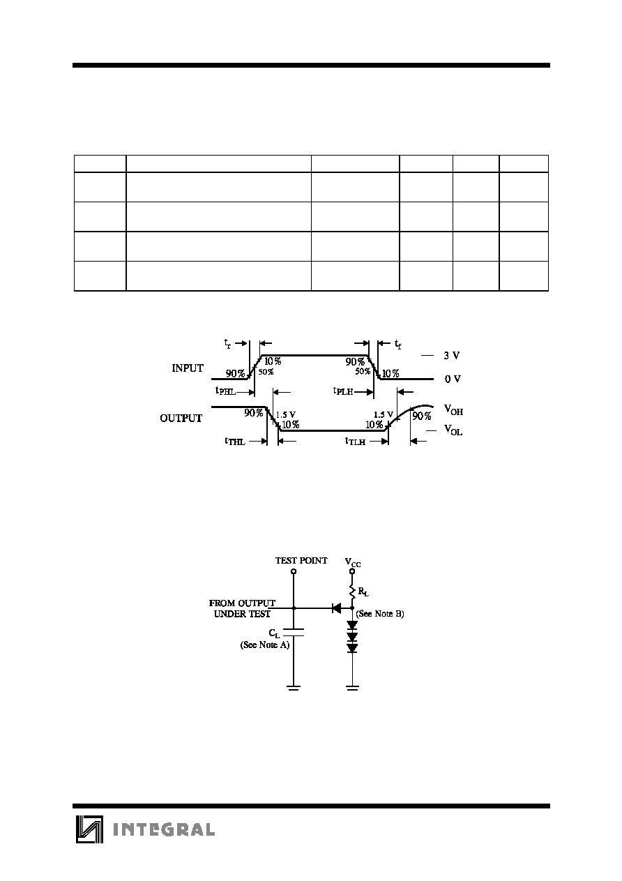
AC ELECTRICAL CHARACTERISTICS
(T = 25
úC, V
CC
= 5.0 V, C
L
= 15 pF,
t
r
=t
f
=5 ns)
Symbol
Parameter
Test Conditions
Min
Max
Unit
t
PLH
Propagation Delay Time, Low-to-High
Level Output (Figure 1)
R
L
=3.9 k
85
ns
t
PHL
Propagation Delay Time, High-to-Low
Level Output (Figure 1)
R
L
=390 k
50
ns
t
TLH
Transition Time, Low-to-High Level
Output (Figure 1)
R
L
=3.9 k
300
ns
t
THL
Transition Time, High-to-Low Level
Output (Figure 1)
R
L
=390 k
24
ns
Figure 1. Switching Waveforms
NOTES A. C
L
includes probe and jig capacitance.
B. All diodes are 1N916 or 1N3064/
Figure 2. Test Circuit