 | –≠–ª–µ–∫—Ç—Ä–æ–Ω–Ω—ã–π –∫–æ–º–ø–æ–Ω–µ–Ω—Ç: IN74AC112 | –°–∫–∞—á–∞—Ç—å:  PDF PDF  ZIP ZIP |
TECHNICAL DATA
127
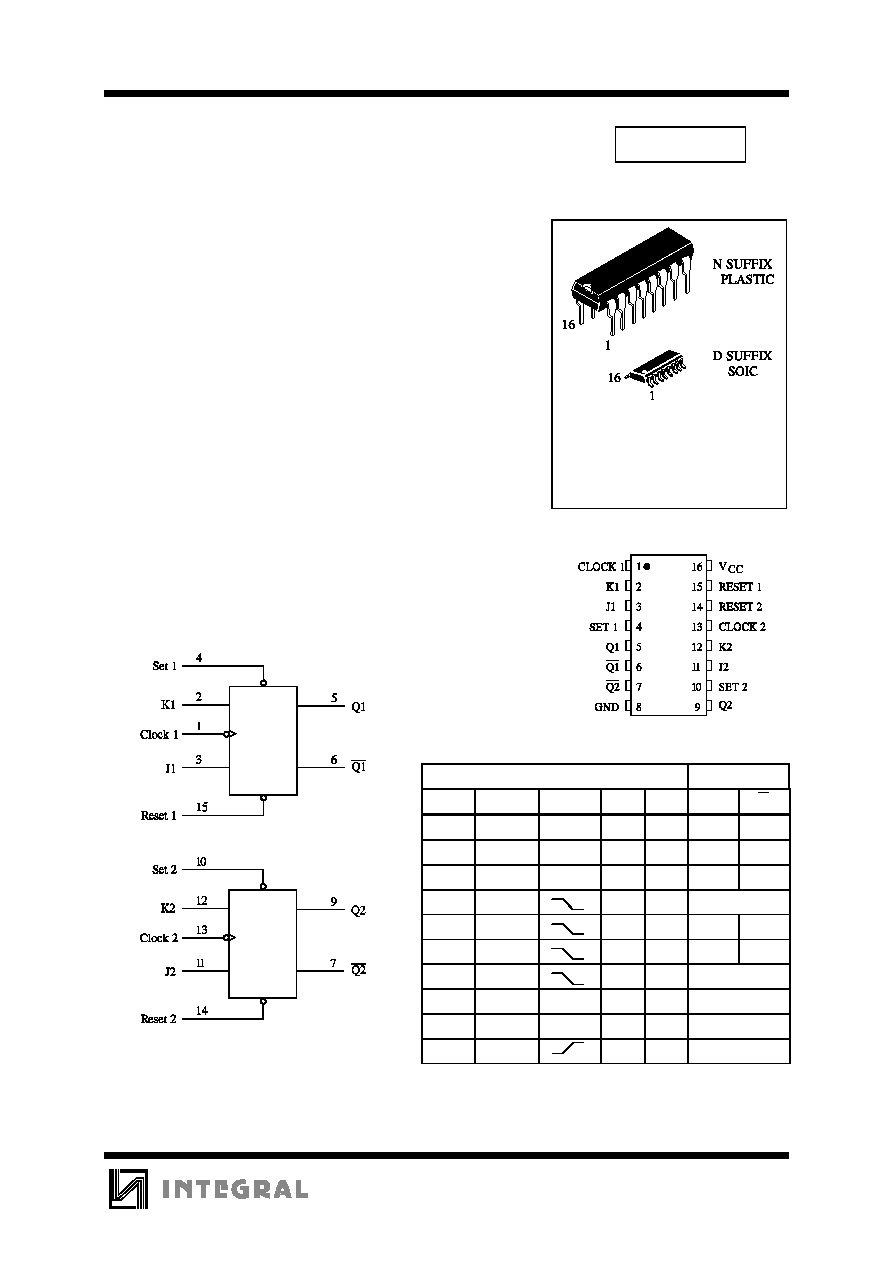
Dual J-K Flip-Flop
with Set and Reset
High-Speed Silicon-Gate CMOS
The IN74AC112 is identical in pinout to the LS/ALS112,
HC/HCT112. The device inputs are compatible with standard CMOS
outputs; with pullup resistors, they are compatible with LS/ALS
outputs.
Each flip-flop is negative-edge clocked and has active-low
asynchronous Set and Reset inputs.
û
Outputs Directly Interface to CMOS, NMOS, and TTL
û
Operating Voltage Range: 2.0 to 6.0 V
û
Low Input Current: 1.0
A; 0.1
A @ 25
ú
C
û
High Noise Immunity Characteristic of CMOS Devices
û
Outputs Source/Sink 24 mA
IN74AC112
ORDERING INFORMATION
IN74AC112N Plastic
IN74AC112D SOIC
T
A
= -40
ú
to 85
ú
C for all
packages
FUNCTION TABLE
Inputs
Outputs
Set
Reset
Clock
J
K
Q
Q
L
H
X
X
X
H
L
H
L
X
X
X
L
H
L
L
X
X
X
L
*
L
*
H
H
L
L
No Change
H
H
L
H
L
H
H
H
H
L
H
L
H
H
H
H
Toggle
H
H
L
X
X
No Change
H
H
H
X
X
No Change
H
H
X
X
No Change
* Both outputs will remain low as long as Set and Reset are
low, but the output states are unpredictable if Set and Reset
go high simultaneously
X = Don't Care
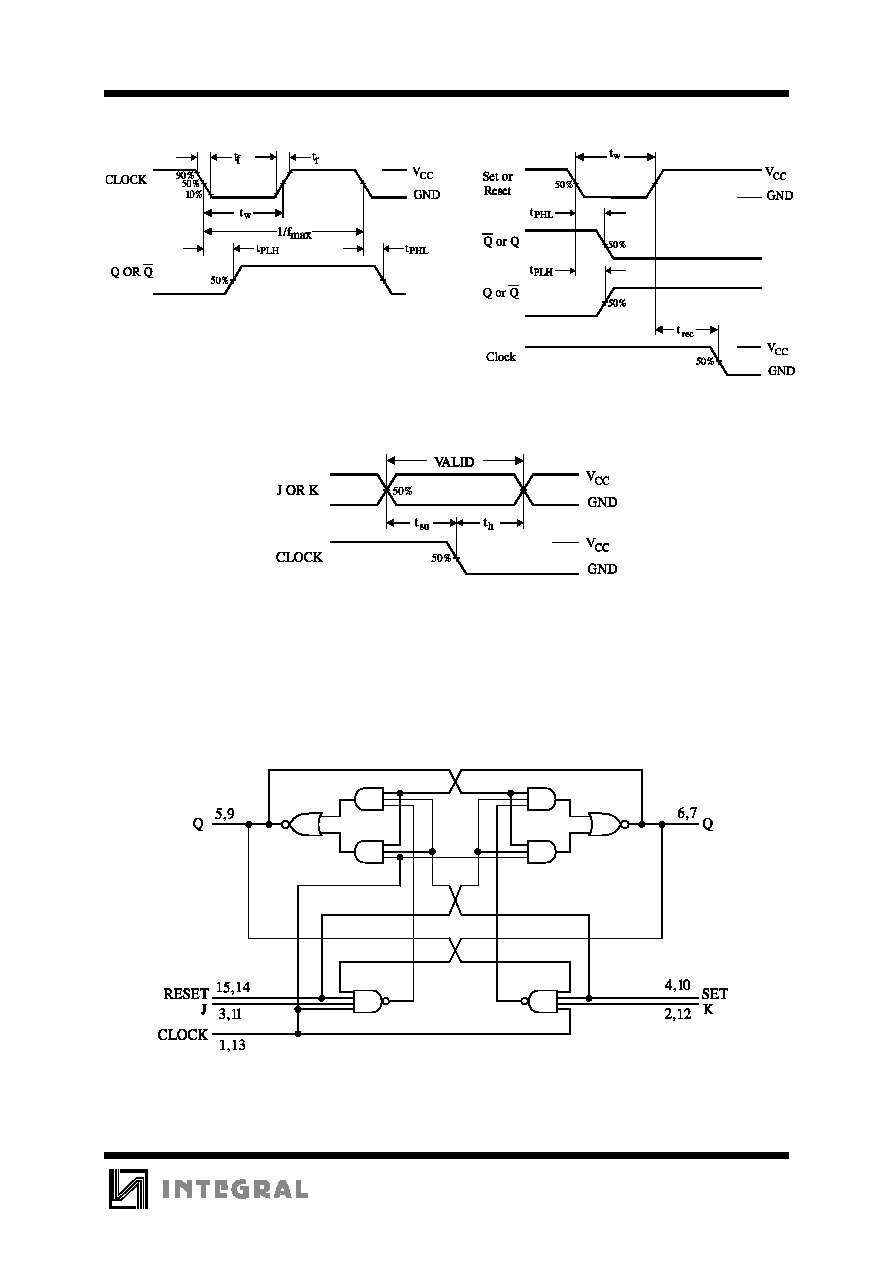
LOGIC DIAGRAM
PIN 16=V
CC
PIN 8 = GND
PIN ASSIGNMENT
IN74AC112
128
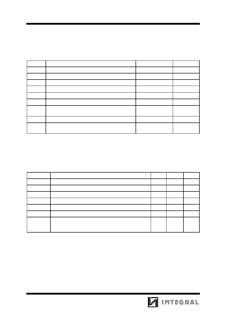
MAXIMUM RATINGS
*
Symbol
Parameter
Value
Unit
V
CC
DC Supply Voltage (Referenced to GND)
-0.5 to +7.0
V
V
IN
DC Input Voltage (Referenced to GND)
-0.5 to V
CC
+0.5
V
V
OUT
DC Output Voltage (Referenced to GND)
-0.5 to V
CC
+0.5
V
I
IN
DC Input Current, per Pin
20
mA
I
OUT
DC Output Sink/Source Current, per Pin
50
mA
I
CC
DC Supply Current, V
CC
and GND Pins
50
mA
P
D
Power Dissipation in Still Air, Plastic DIP+
SOIC Package+
750
500
mW
Tstg
Storage Temperature
-65 to +150
ú
C
T
L
Lead Temperature, 1 mm from Case for 10 Seconds
(Plastic DIP or SOIC Package)
260
ú
C
*
Maximum Ratings are those values beyond which damage to the device may occur.
Functional operation should be restricted to the Recommended Operating Conditions.
+Derating - Plastic DIP: - 10 mW/
ú
C from 65
ú
to 125
ú
C
SOIC Package: : - 7 mW/
ú
C from 65
ú
to 125
ú
C
RECOMMENDED OPERATING CONDITIONS
Symbol
Parameter
Min
Max
Unit
V
CC
DC Supply Voltage (Referenced to GND)
2.0
6.0
V
V
IN
, V
OUT
DC Input Voltage, Output Voltage (Referenced to GND)
0
V
CC
V
T
J
Junction Temperature (PDIP)
140
ú
C
T
A
Operating Temperature, All Package Types
-40
+85
ú
C
I
OH
Output Current - High
-24
mA
I
OL
Output Current - Low
24
mA
t
r
, t
f
Input Rise and Fall Time
*
(except Schmitt Inputs)
V
CC
=3.0 V
V
CC
=4.5 V
V
CC
=5.5 V
0
0
0
150
40
25
ns/V
*
V
IN
from 30% to 70% V
CC
This device contains protection circuitry to guard against damage due to high static voltages or electric
fields. However, precautions must be taken to avoid applications of any voltage higher than maximum rated
voltages to this high-impedance circuit. For proper operation, V
IN
and V
OUT
should be constrained to the range
GND
ò
(V
IN
or V
OUT
)
ò
V
CC
.
Unused inputs must always be tied to an appropriate logic voltage level (e.g., either GND or V
CC
).
Unused outputs must be left open.
IN74AC112
129
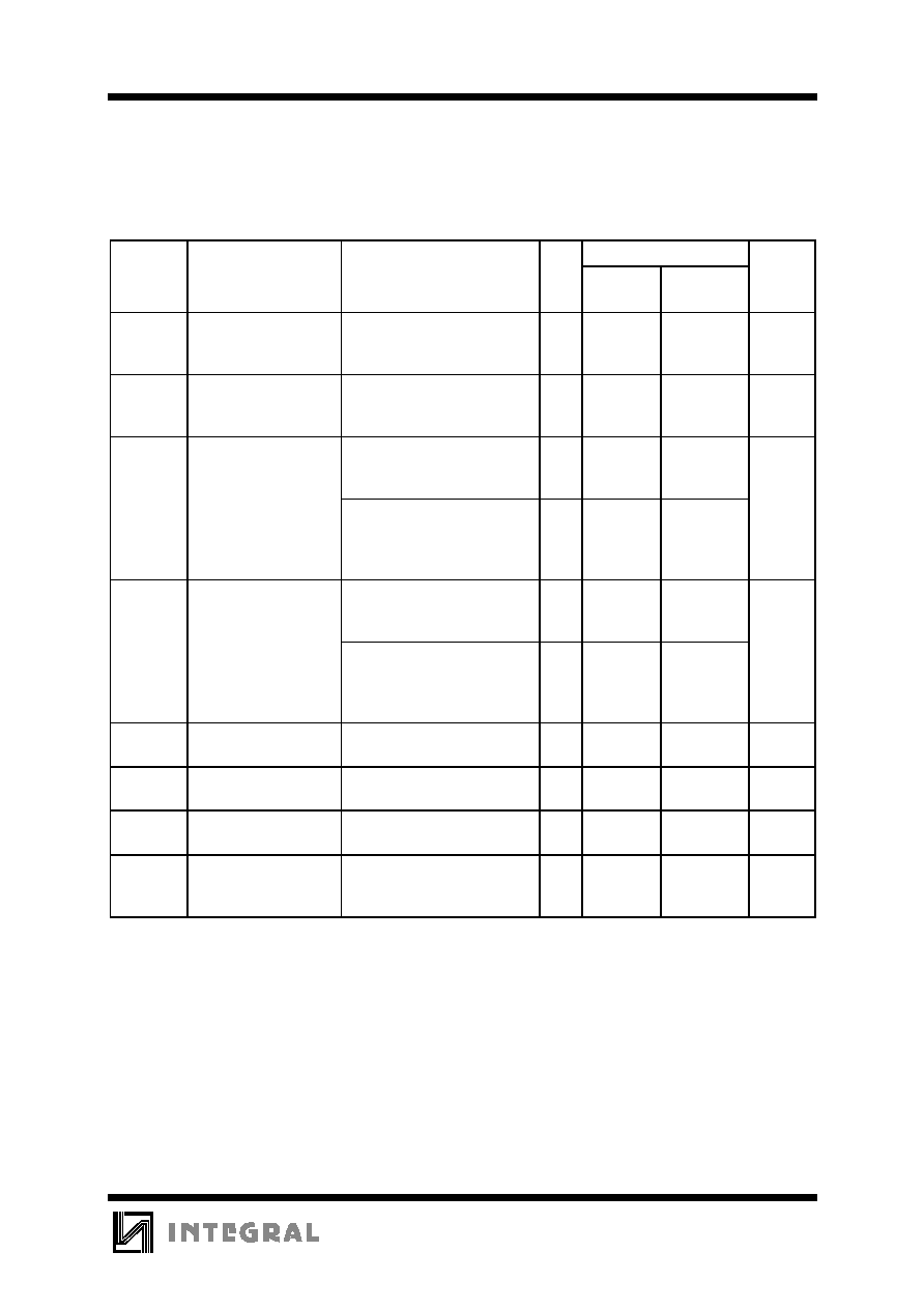
DC ELECTRICAL CHARACTERISTICS
(Voltages Referenced to GND)
V
CC
Guaranteed Limits
Symbol
Parameter
Test Conditions
V
25
ú
C
-40
ú
C to
85
ú
C
Unit
V
IH
Minimum High-Level
Input Voltage
V
OUT
=0.1 V or V
CC
-0.1 V
3.0
4.5
5.5
2.1
3.15
3.85
2.1
3.15
3.85
V
V
IL
Maximum Low -
Level Input Voltage
V
OUT
=0.1 V or V
CC
-0.1 V
3.0
4.5
5.5
0.9
1.35
1.65
0.9
1.35
1.65
V
V
OH
Minimum High-Level
Output Voltage
I
OUT
ò
-50
A
3.0
4.5
5.5
2.9
4.4
5.4
2.9
4.4
5.4
V
*
V
IN
=V
IH
or V
IL
I
OH
=-12 mA
I
OH
=-24 mA
I
OH
=-24 mA
3.0
4.5
5.5
2.56
3.86
4.86
2.46
3.76
4.76
V
OL
Maximum Low-Level
Output Voltage
I
OUT
ò
50
A
3.0
4.5
5.5
0.1
0.1
0.1
0.1
0.1
0.1
V
*
V
IN
=V
IH
or V
IL
I
OL
=12 mA
I
OL
=24 mA
I
OL
=24 mA
3.0
4.5
5.5
0.36
0.36
0.36
0.44
0.44
0.44
I
IN
Maximum Input
Leakage Current
V
IN
=V
CC
or GND
5.5
0.1
1.0
A
I
OLD
+Minimum Dynamic
Output Current
V
OLD
=1.65 V Max
5.5
75
mA
I
OHD
+Minimum Dynamic
Output Current
V
OHD
=3.85 V Min
5.5
-75
mA
I
CC
Maximum Quiescent
Supply Current
(per Package)
V
IN
=V
CC
or GND
5.5
4.0
40
A
*
All outputs loaded; thresholds on input associated with output under test.
+Maximum test duration 2.0 ms, one output loaded at a time.
Note: I
IN
and I
CC
@ 3.0 V are guaranteed to be less than or equal to the respective limit @ 5.5 V V
CC
IN74AC112
130
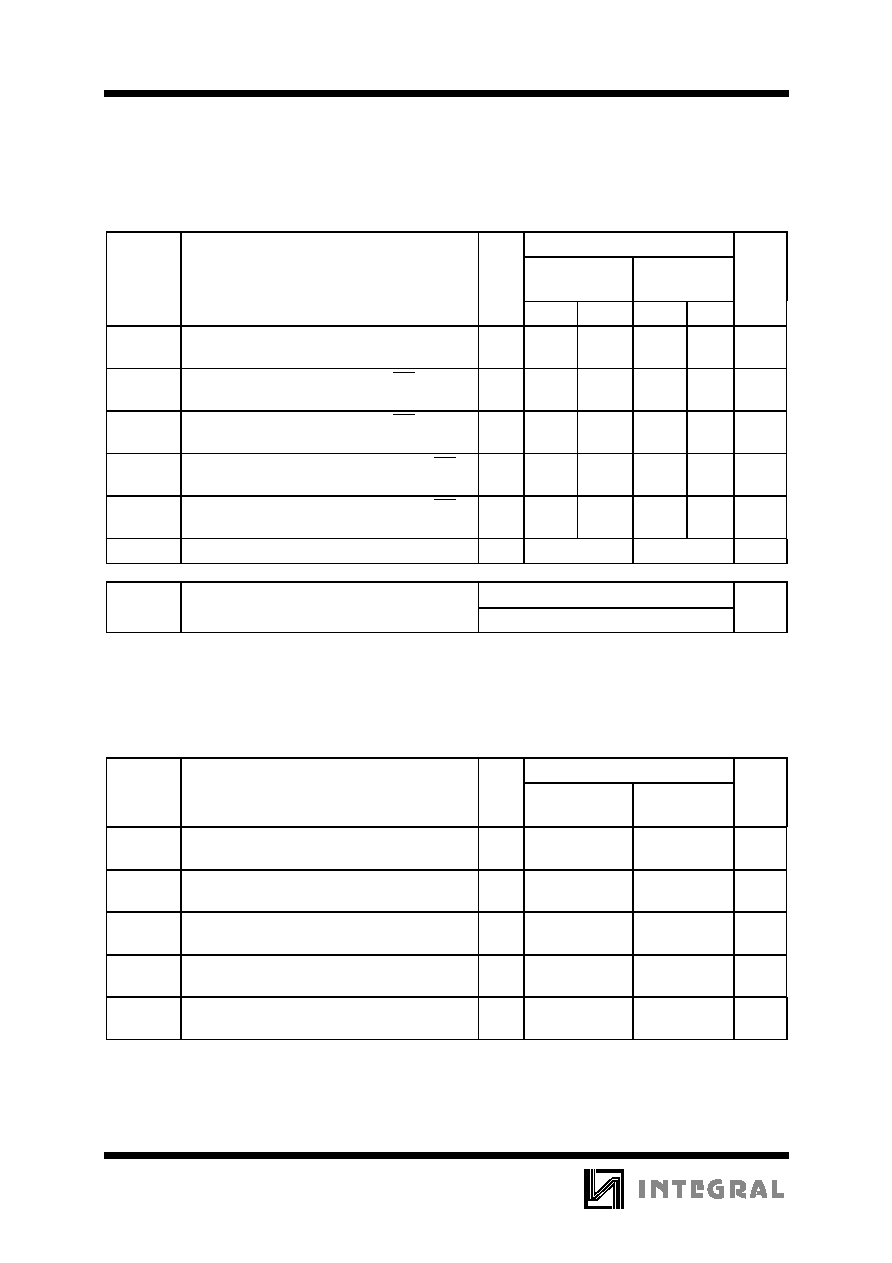
AC ELECTRICAL CHARACTERISTICS
(C
L
=50pF,Input t
r
=t
f
=3.0 ns)
V
CC
*
Guaranteed Limits
Symbol
Parameter
V
25
ú
C
-40
ú
C to
85
ú
C
Unit
Min
Max
Min
Max
f
max
Maximum Clock Frequency (Figure 1)
3.3
5.0
145
145
125
125
MHz
t
PLH
Propagation Delay, Clock to Q or Q
(Figure 1)
3.3
5.0
1.0
1.0
16.0
13.0
1.0
1.0
17.0
13.5
ns
t
PHL
Propagation Delay, Clock to Q or Q
(Figure 1)
3.3
5.0
1.0
1.0
16.0
13.0
1.0
1.0
16.5
13.5
ns
t
PLH
Propagation Delay, Set or Reset to Q or Q
(Figure 2)
3.3
5.0
1.0
1.0
11.0
9.5
1.0
1.0
11.5
10.0
ns
t
PHL
Propagation Delay, Set or Reset to Q or Q
(Figure 2)
3.3
5.0
1.0
1.0
11.0
9.5
1.0
1.0
11.5
10.0
ns
C
IN
Maximum Input Capacitance
5.0
4.5
4.5
pF
Typical @25
ú
C,V
CC
=5.0 V
C
PD
Power Dissipation Capacitance
35
pF
*
Voltage Range 3.3 V is 3.3 V
0.3 V
Voltage Range 5.0 V is 5.0 V
0.5 V
TIMING REQUIREMENTS
(C
L
=50pF,Input t
r
=t
f
=3.0 ns)
V
CC
*
Guaranteed Limits
Symbol
Parameter
V
25
ú
C
-40
ú
C to
85
ú
C
Unit
t
su
Minimum Setup Time, J or K to Clock (Figure
3)
3.3
5.0
6.5
4.5
7.5
5.0
ns
t
h
Minimum Hold Time, Clock to J or K (Figure
3)
3.3
5.0
0
0
0
0
ns
t
w
Minimum Pulse Width, Clock (Figure 1)
3.3
5.0
6.0
5.0
6.5
5.5
ns
t
w
Minimum Pulse Width,Set or Reset
(Figure 2)
3.3
5.0
6.5
5.0
7.5
5.5
ns
t
rec
Minimum Recovery Time, Set or Reset to
Clock (Figure 2)
3.3
5.0
0
0
0
0
ns
*
Voltage Range 3.3 V is 3.3 V
0.3 V
Voltage Range 5.0 V is 5.0 V
0.5 V
IN74AC112
131
Figure 1. Switching Waveform
Figure 2. Switching Waveform
Figure 3. Switching Waveform
EXPANDED LOGIC DIAGRAM