
TECHNICAL DATA
336
8-Input Data Selector/Multiplexer
with 3-State Outputs
High-Speed Silicon-Gate CMOS
The IN74AC251 is identical in pinout to the LS/ALS251,
HC/HCT251. The device inputs are compatible with standard CMOS
outputs; with pullup resistors, they are compatible with LS/ALS
outputs.
The device selects one of the eight binary Data Inputs, as
determined by the Address Inputs. The Output Enable pin must be at a
low level for the selected data to appear at the outputs. If Output
Enable is high, the Y and the Y outputs are in the high-impedance
state. This 3-State feature allows the IN74AC251 to be used in bus-
oriented systems.
ћ
Outputs Directly Interface to CMOS, NMOS, and TTL
ћ
Operating Voltage Range: 2.0 to 6.0 V
ћ
Low Input Current: 1.0
A; 0.1
A @ 25
њ
C
ћ
High Noise Immunity Characteristic of CMOS Devices
ћ
Outputs Source/Sink 24 mA
IN74AC251
ORDERING INFORMATION
IN74AC251N Plastic
IN74AC251D SOIC
T
A
= -40
њ
to 85
њ
C for all
packages
PIN ASSIGNMENT
FUNCTION TABLE
Inputs
Outputs
A2 A1
A0
Output
Enable
Y
Y
X
X
X
H
Z
Z
L
L
L
L
D0
D0
L
L
H
L
D1
D1
L
H
L
L
D2
D2
L
H
H
L
D3
D3
H
L
L
L
D4
D4
H
L
H
L
D5
D5
H
H
L
L
D6
D6
H
H
H
L
D7
D7
D0,D1...D7=the level of the respective D
input
Z = high-impedance state
X = don't care
LOGIC DIAGRAM
PIN 16 =V
CC
PIN 8 = GND
IN74AC251
337
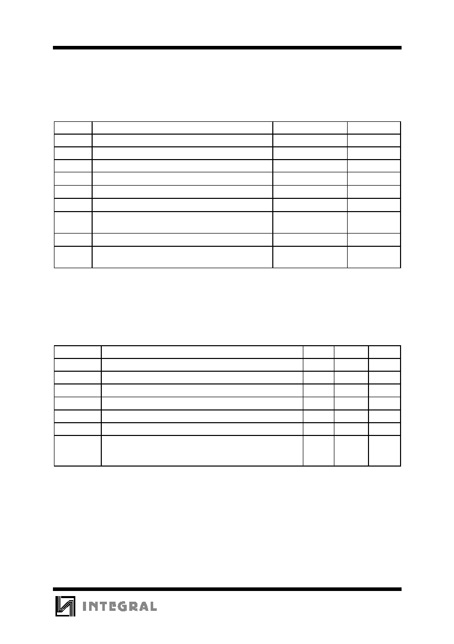
MAXIMUM RATINGS
*
Symbol
Parameter
Value
Unit
V
CC
DC Supply Voltage (Referenced to GND)
-0.5 to +7.0
V
V
IN
DC Input Voltage (Referenced to GND)
-0.5 to V
CC
+0.5
V
V
OUT
DC Output Voltage (Referenced to GND)
-0.5 to V
CC
+0.5
V
I
IN
DC Input Current, per Pin
20
mA
I
OUT
DC Output Sink/Source Current, per Pin
50
mA
I
CC
DC Supply Current, V
CC
and GND Pins
50
mA
P
D
Power Dissipation in Still Air, Plastic DIP+
SOIC Package+
750
500
mW
Tstg
Storage Temperature
-65 to +150
њ
C
T
L
Lead Temperature, 1 mm from Case for 10 Seconds
(Plastic DIP or SOIC Package)
260
њ
C
*
Maximum Ratings are those values beyond which damage to the device may occur.
Functional operation should be restricted to the Recommended Operating Conditions.
+Derating - Plastic DIP: - 10 mW/
њ
C from 65
њ
to 125
њ
C
SOIC Package: : - 7 mW/
њ
C from 65
њ
to 125
њ
C
RECOMMENDED OPERATING CONDITIONS
Symbol
Parameter
Min
Max
Unit
V
CC
DC Supply Voltage (Referenced to GND)
2.0
6.0
V
V
IN
, V
OUT
DC Input Voltage, Output Voltage (Referenced to GND)
0
V
CC
V
T
J
Junction Temperature (PDIP)
140
њ
C
T
A
Operating Temperature, All Package Types
-40
+85
њ
C
I
OH
Output Current - High
-24
mA
I
OL
Output Current - Low
24
mA
t
r
, t
f
Input Rise and Fall Time
*
(except Schmitt Inputs)
V
CC
=3.0 V
V
CC
=4.5 V
V
CC
=5.5 V
0
0
0
150
40
25
ns/V
*
V
IN
from 30% to 70% V
CC
This device contains protection circuitry to guard against damage due to high static voltages or electric
fields. However, precautions must be taken to avoid applications of any voltage higher than maximum rated
voltages to this high-impedance circuit. For proper operation, V
IN
and V
OUT
should be constrained to the range
GND