
IN74ACT192
1
P
RESETTABLE
BCD/D
ECADE
UP/DOWN
C
OUNTER
High-Speed Silicon-Gate CMOS
The IN74ACT192 is identical in pinout to the LS/ALS192,
HC/HCT192. The IN74ACT192 may be used as a level converter
for interfacing TTL or NMOS outputs to High Speed CMOS
inputs.
The counter has two separate clock inputs, a Count Up Clock
and Count Down Clock inputs. The direction of counting is
determined by which input is clocked. The outputs change state
synchronous with the LOW-to-HIGH transitions on the clock
inputs. This counter may be preset by entering the desired data
on the P0, P1, P2, P3 input. When the Parallel Load input is
taken low the data is loaded independently of either clock input.
This feature allows the counters to be used as devide-by-n by
modifying the count lenght with the preset inputs. In addition the
counter can also be cleared. This is accomplished by inputting a
high on the Master Reset input. All 4 internal stages are set to
low independently of either clock input.Both a Terminal Count
Down (TC
D
) and Terminal Count Up (TC
U
) Outputs are provided
to enable cascading of both up and down counting functions.
The TC
D
output produces a negative going pulse when the
counter underflows and TC
U
outputs a pulse when the
counter overflows. The counter can be cascaded by
connecting the TC
U
and TC
D
outputs of one device to the
Count Up Clock and Count Down Clock inputs, respectively,
of the next device.
� TTL/NMOS Compatible Input Levels
� Outputs Directly Interface to CMOS, NMOS, and TTL
� Operating Voltage Range: 4.5 to 5.5 V
� Low Input Current: 1.0 A; 0.1 A @ 25�C
� Outputs Source/Sink 24 mA
ORDERING INFORMATION
IN74ACT192N Plastic
IN74ACT192D SOIC
T
A
= -40
� to 85� C for all
packages
PIN ASSIGNMENT
LOGIC DIAGRAM
PIN 16 =V
CC
PIN 8 = GND
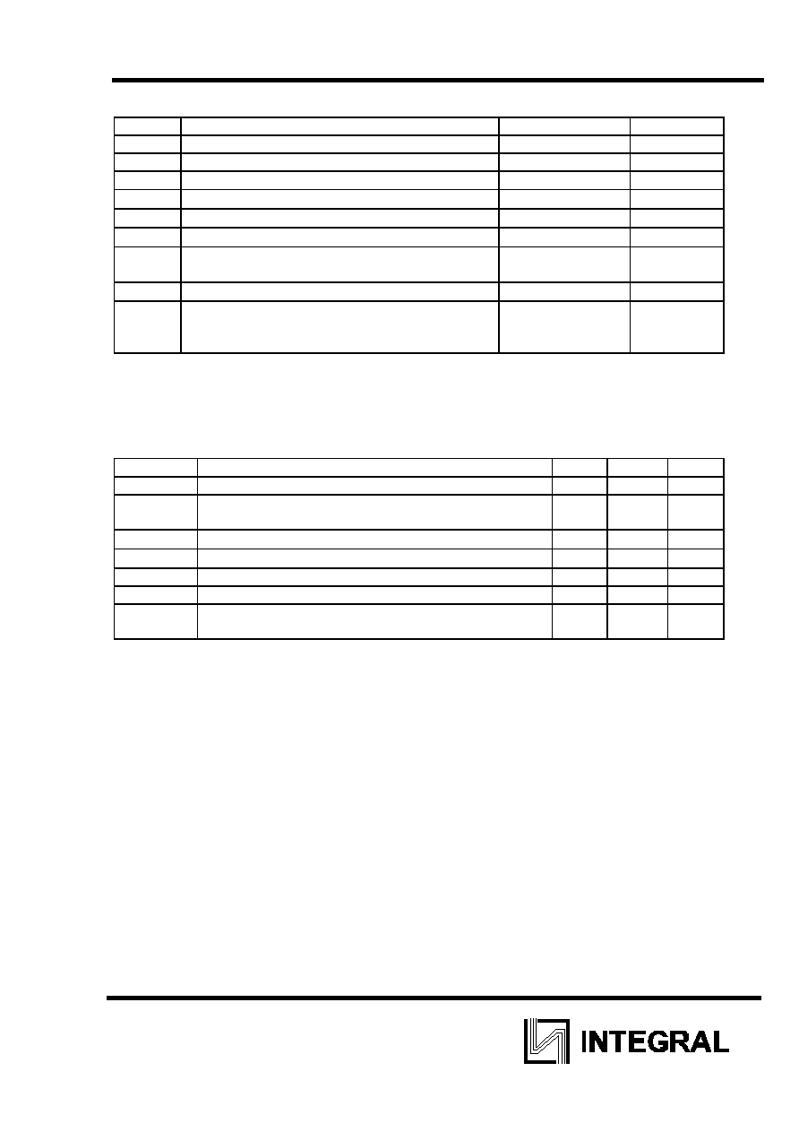
IN74ACT192
2
MAXIMUM RATINGS
*
Symbol Parameter
Value
Unit
V
CC
DC Supply Voltage (Referenced to GND)
-0.5 to +7.0
V
V
IN
DC Input Voltage (Referenced to GND)
-0.5 to V
CC
+0.5
V
V
OUT
DC Output Voltage (Referenced to GND)
-0.5 to V
CC
+0.5
V
I
IN
DC Input Current, per Pin
20
mA
I
OUT
DC Output Sink/Source Current, per Pin
50
mA
I
CC
DC Supply Current, V
CC
and GND Pins
50
mA
P
D
Power Dissipation in Still Air, Plastic DIP+
SOIC Package+
750
500
mW
Tstg
Storage Temperature
-65 to +150
�C
T
L
Lead Temperature, 1 mm from Case for 10
Seconds
(Plastic DIP or SOIC Package)
260
�C
*
Maximum Ratings are those values beyond which damage to the device may occur.
Functional operation should be restricted to the Recommended Operating Conditions.
+Derating - Plastic DIP: - 10 mW/
�C from 65� to 125�C
SOIC Package: : - 7 mW/
�C from 65� to 125�C
RECOMMENDED OPERATING CONDITIONS
Symbol Parameter Min
Max
Unit
V
CC
DC Supply Voltage (Referenced to GND)
4.5
5.5
V
V
IN
, V
OUT
DC Input Voltage, Output Voltage (Referenced to
GND)
0 V
CC
V
T
J
Junction Temperature (PDIP)
140
�C
T
A
Operating Temperature, All Package Types
-40
+85
�C
I
OH
Output Current - High
-24
mA
I
OL
Output Current - Low
24
mA
t
r
, t
f
Input Rise and Fall Time
*
(except Schmitt Inputs)
V
CC
=4.5 V
V
CC
=5.5 V
0
0
10
8.0
ns/V
*
V
IN
from 0.8 V to 2.0 V
This device contains protection circuitry to guard against damage due to high static
voltages or electric fields. However, precautions must be taken to avoid applications of any voltage
higher than maximum rated voltages to this high-impedance circuit. For proper operation, V
IN
and
V
OUT
should be constrained to the range GND
�(V
IN
or V
OUT
)
�V
CC
.
Unused inputs must always be tied to an appropriate logic voltage level (e.g., either GND or
V
CC
). Unused outputs must be left open.
IN74ACT192
3
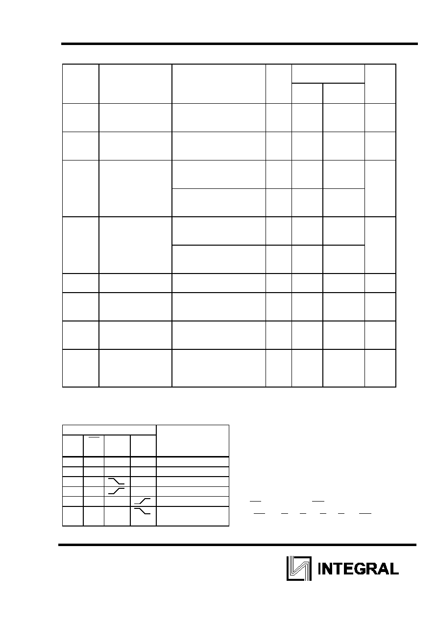
DC ELECTRICAL CHARACTERISTICS(Voltages Referenced to GND)
V
CC
Guaranteed
Limits
Symbol Parameter Test
Conditions
V
25
�C -40�C to
85
�C
Unit
V
IH
Minimum High-
Level Input
Voltage
V
OUT
=0.1 V or V
CC
-0.1 V
4.5
5.5
2.0
2.0
2.0
2.0
V
V
IL
Maximum Low -
Level Input
Voltage
V
OUT
=0.1 V or V
CC
-0.1 V
4.5
5.5
0.8
0.8
0.8
0.8
V
V
OH
Minimum High-
Level Output
Voltage
I
OUT
� -50 A
4.5
5.5
4.4
5.4
4.4
5.4
V
*
V
IN
=V
IH
or V
IL
I
OH
=-24 mA
I
OH
=-24 mA
4.5
5.5
3.86
4.86
3.76
4.76
V
OL
Maximum Low-
Level Output
Voltage
I
OUT
� 50 A
4.5
5.5
0.1
0.1
0.1
0.1
V
*
V
IN
=V
IH
I
OL
=24 mA
I
OL
=24 mA
4.5
5.5
0.36
0.36
0.44
0.44
I
IN
Maximum
Input
Leakage Current
V
IN
=V
CC
or GND
5.5
0.1
1.0
A
I
OLD
+Minimum
Dynamic Output
Current
V
OLD
=1.65 V Max
5.5
75
mA
I
OHD
+Minimum
Dynamic Output
Current
V
OHD
=3.85 V Min
5.5
-75
mA
I
CC
Maximum
Quiescent Supply
Current
(per Package)
V
IN
=V
CC
or GND
5.5
8.0
80
A
*
All outputs loaded; thresholds on input associated with output under test.
+Maximum test duration 2.0 ms, one output loaded at a time.
FUNCTION TABLE
Inputs Mode
MR
PL
CP
U
CP
D
H X X X Reset(Asyn.)
L L X X Preset(Asyn.)
L H H
No
Count
L H H
Count
Up
L H H
Count
Down
L H H
No
Count
The IN74ACT192 can be preset to any
state, but will not count beyond 9. If preset to
state 10, 11, 12, 13, 14 or 15, it will follow the
sequence 10, 11, 6: 12, 13, 4: 14, 15, 2 if
counting Up, and follow the sequence 15, 14,
13, 12, 11, 10, 9 if counting Down.
Logic equations
For Terminal Count:
U
TC
= Q
0
� Q
3
�
U
CP
D
TC
=
0
Q
�
1
Q
�
2
Q
�
3
Q
�
D
CP
X = don't care

IN74ACT192
4
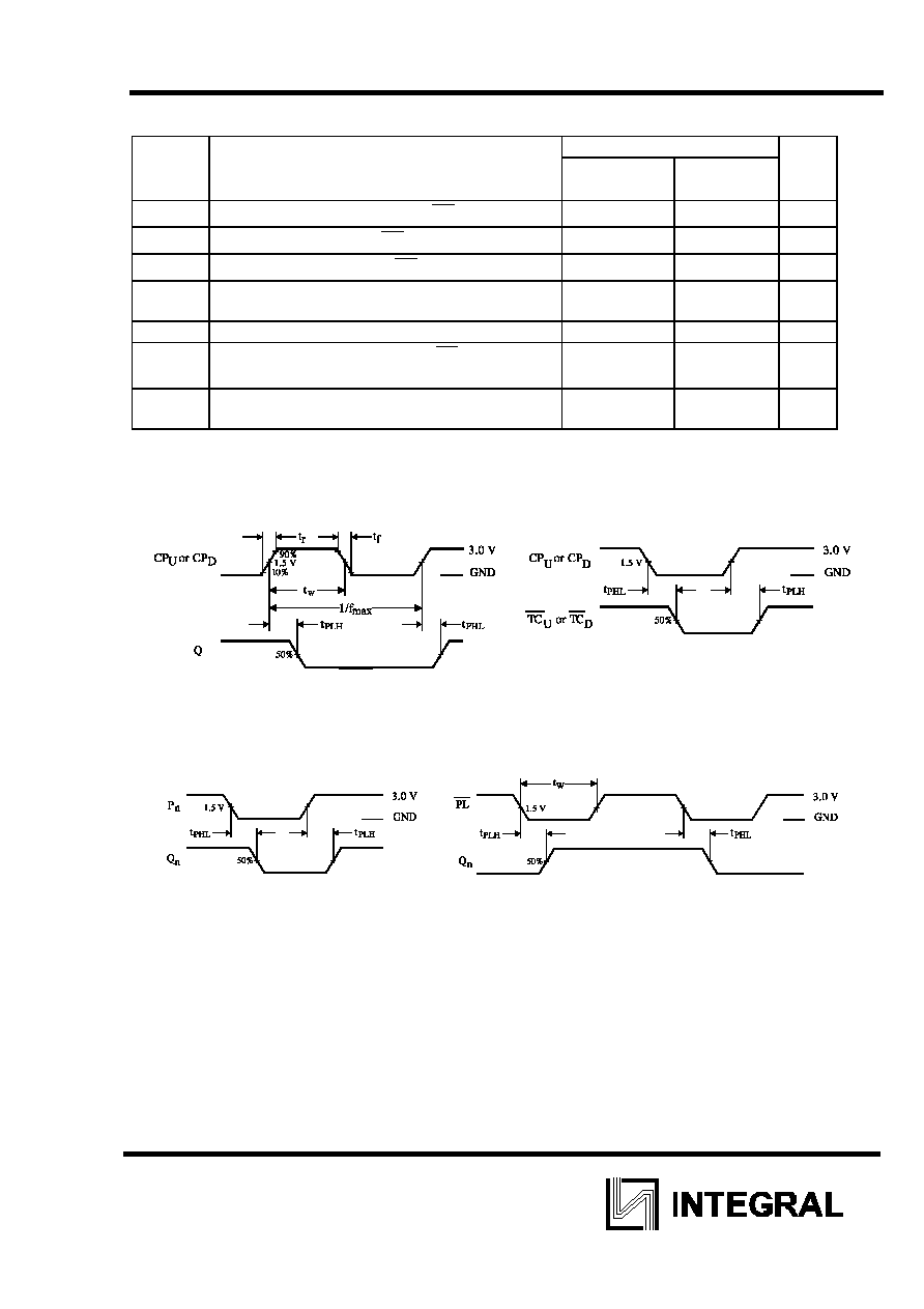
AC ELECTRICAL CHARACTERISTICS(V
CC
=5.0 V
10%, C
L
=50pF,Input t
r
=t
f
=3.0 ns)
Guaranteed
Limits
Symbol Parameter
25
�C -40�C to
85
�C
Unit
Min
Max
Min
Max
f
max
Maximum Clock Frequency (Figure 1)
100
80
MHz
t
PLH
Propagation Delay, CP
U
or to
U
TC
or
D
TC
(Figure 2)
15 16.5 ns
t
PHL
Propagation Delay, CP
U
or CP
D
to
U
TC
or
D
TC
(Figure 2)
14 15.5 ns
t
PLH
Propagation
Delay,
CP
U
or CP
D
to Q
n
(Figure 1)
12 13.5 ns
t
PHL
Propagation
Delay,
CP
U
or CP
D
to Q
n
(Figure 1)
12 13.5 ns
t
PLH
Propagation Delay, P
n
to Q
n
(Figure 3)
12
13.5
ns
t
PHL
Propagation Delay, P
n
to Q
n
(Figure 3)
12
13.5
ns
t
PLH
Propagation Delay,
PL
to Q
n
(Figure 4)
12 13.5 ns
t
PHL
Propagation Delay,
PL
to Q
n
(Figure 4)
15 16.5 ns
t
PHL
Propagation Delay, MR to Q
n
(Figure 5)
15
16.5
ns
t
PLH
Propagation Delay, MR to
U
TC
(Figure 6)
14 15.5 ns
t
PHL
Propagation Delay, MR to
D
TC
(Figure 6)
14 15.5 ns
t
PLH
Propagation Delay,
PL
to
U
TC
or
D
TC
(Figure 6)
15 16.5 ns
t
PHL
Propagation Delay,
PL
to
U
TC
or
D
TC
(Figure 6)
11 12.5 ns
t
PLH
Propagation Delay, P
n
to
U
TC
or
D
TC
(Figure 6)
15 16.5 ns
t
PHL
Propagation Delay, P
n
to
U
TC
or
D
TC
(Figure 6)
15 16.5 ns
C
IN
Maximum Input Capacitance
4.5
4.5
pF
Typical @25
�C,V
CC
=5.0
V
C
PD
Power Dissipation Capacitance
45
pF
IN74ACT192
5
TIMING REQUIREMENTS(C
L
=50pF, Input t
r
=t
f
=3.0 ns, V
CC
=5.0 V
10%)
Guaranteed
Limits
Symbol Parameter
25
�C -40�C to
85
�C
Unit
t
su
Minimum Setup Time, P
n
to
PL
(Figure 7)
8 9
ns
t
h
Minimum Hold Time,
PL
to P
n
(Figure 7)
-1.0 -1.0
ns
t
w
Minimum Pulse Width,
PL
(Figure 4)
14 15
ns
t
w
Minimum Pulse Width, CP
U
or CP
D
(Figure 1)
10 11
ns
t
w
Minimum Pulse Width, MR (Figure 5)
12
14
ns
t
rec
Minimum Recovery Time,
PL
to CP
U
or
CP
D
(Figure 5)
8 9
ns
t
rec
Minimum Recovery Time, MR to CP
U
or
CP
D
(Figure 5)
14 16
ns
Figure 1. Switching Waveforms
Figure 2. Switching Waveforms
Figure 3. Switching Waveforms
Figure 4. Switching Waveforms