IN74ACT651
1
O
CTAL
3-S
TATE
B
US
T
RANSCEIVERS
AND
D
F
LIP
-F
LOPS
High-Speed Silicon-Gate CMOS
The IN74ACT651 is identical in pinout to the LS/ALS651,
HC/HCT651. The IN74ACT651 may be used as a level converter
for interfacing TTL or NMOS outputs to High Speed CMOS
inputs.
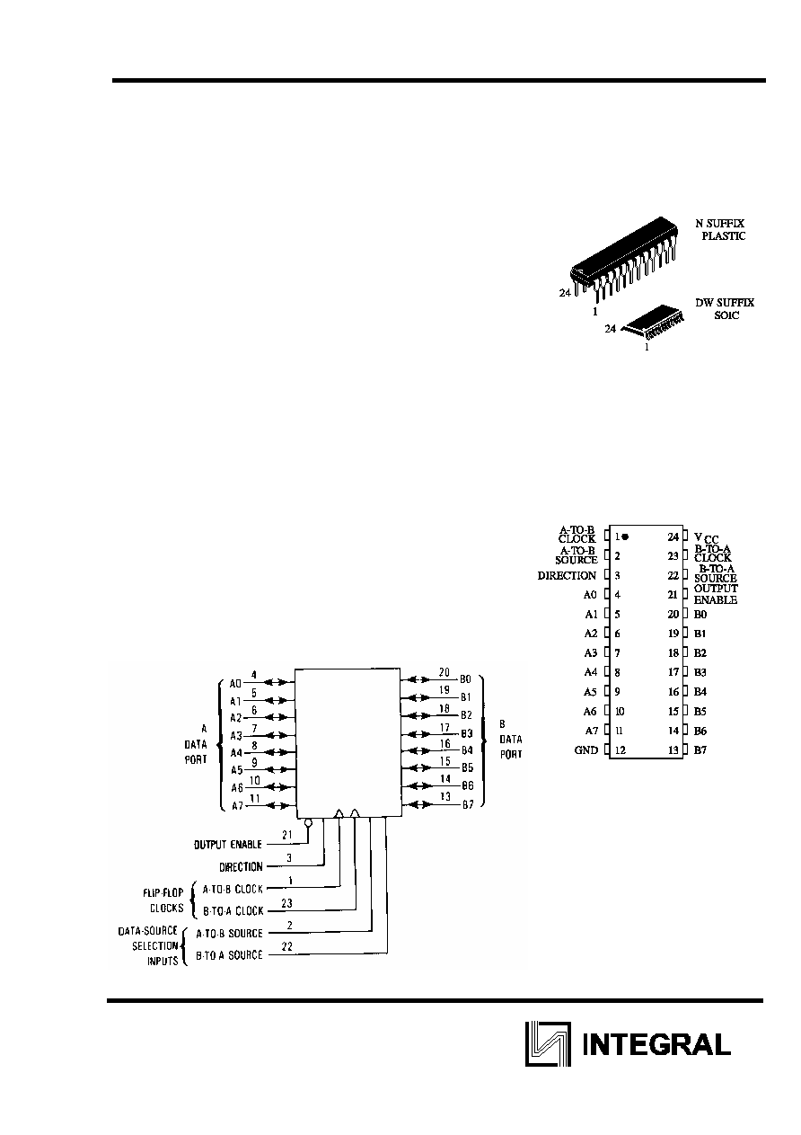
These devices consists of bus transceiver circuits, D-type flip-
flop, and control circuitry arranged for multiplex transmission of
data directly from the data bus or from the internal storage
registers. Direction and Output Enable are provided to select the
read-time or stored data function. Data on the A or B Data bus,
or both, can be stored in the internal D flip-flops by low-to-high
transitions at the appropriate clock pins (A-to-B Clock or B-to-A
Clock) regardless of the select or enable or enable control pins.
When A-to-B Source and B-to-A Source are in the real-time
transfer mode, it is also possible to store data without using the
internal D-type flip-flops by simultaneously enabling Direction
and Output Enable. In this configuration each output reinforces
its input. Thus, when all other data sources to the two sets of bus
lines are at high impedance, each set of bus lines will remain
at its last state.
The IN74ACT651 has inverted outputs.
û TTL/NMOS Compatible Input Levels
û Outputs Directly Interface to CMOS, NMOS, and TTL
û Operating Voltage Range: 4.5 to 5.5 V
û Low Input Current: 1.0 A; 0.1 A @ 25úC
û Outputs Source/Sink 24 mA
ORDERING INFORMATION
IN74ACT651N Plastic
IN74ACT651DW SOIC
T
A
= -40
ú to 85ú C for all
packages
PIN ASSIGNMENT
LOGIC DIAGRAM
PIN 24=V
CC
PIN 12 = GND

IN74ACT651
2
MAXIMUM RATINGS
*
Symbol Parameter
Value
Unit
V
CC
DC Supply Voltage (Referenced to GND)
-0.5 to +7.0
V
V
IN
DC Input Voltage (Referenced to GND)
-0.5 to V
CC
+0.5
V
V
OUT
DC Output Voltage (Referenced to GND)
-0.5 to V
CC
+0.5
V
I
IN
DC Input Current, per Pin
20
mA
I
OUT
DC Output Sink/Source Current, per Pin
50
mA
I
CC
DC Supply Current, V
CC
and GND Pins
50
mA
P
D
Power Dissipation in Still Air, Plastic DIP+
SOIC Package+
750
500
mW
Tstg
Storage Temperature
-65 to +150
úC
T
L
Lead Temperature, 1 mm from Case for 10
Seconds
(Plastic DIP or SOIC Package)
260
úC
*
Maximum Ratings are those values beyond which damage to the device may occur.
Functional operation should be restricted to the Recommended Operating Conditions.
+Derating - Plastic DIP: - 10 mW/
úC from 65ú to 125úC
SOIC Package: : - 7 mW/
úC from 65ú to 125úC
RECOMMENDED OPERATING CONDITIONS
Symbol Parameter Min
Max
Unit
V
CC
DC Supply Voltage (Referenced to GND)
4.5
5.5
V
V
IN
, V
OUT
DC Input Voltage, Output Voltage (Referenced to
GND)
0 V
CC
V
T
J
Junction Temperature (PDIP)
140
úC
T
A
Operating Temperature, All Package Types
-40
+85
úC
I
OH
Output Current - High
-24
mA
I
OL
Output Current - Low
24
mA
t
r
, t
f
Input Rise and Fall Time
*
(except Schmitt Inputs)
V
CC
=4.5 V
V
CC
=5.5 V
0
0
10
8.0
ns/V
*
V
IN
from 0.8 V to 2.0 V
This device contains protection circuitry to guard against damage due to high static
voltages or electric fields. However, precautions must be taken to avoid applications of any voltage
higher than maximum rated voltages to this high-impedance circuit. For proper operation, V
IN
and
V
OUT
should be constrained to the range GND
ò(V
IN
or V
OUT
)
òV
CC
.
Unused inputs must always be tied to an appropriate logic voltage level (e.g., either GND or
V
CC
). Unused outputs must be left open.

IN74ACT651
3
DC ELECTRICAL CHARACTERISTICS(Voltages Referenced to GND)
V
CC
Guaranteed
Limits
Symbol Parameter
Test
Conditions
V 25
úC -40úC to
85
úC
Unit
V
IH
Minimum
High-
Level Input
Voltage
V
OUT
=0.1 V or V
CC
-0.1 V
4.5
5.5
2.0
2.0
2.0
2.0
V
V
IL
Maximum Low -
Level Input
Voltage
V
OUT
=0.1 V or V
CC
-0.1 V
4.5
5.5
0.8
0.8
0.8
0.8
V
V
OH
Minimum
High-
Level Output
Voltage
I
OUT
ò -50 A
4.5
5.5
4.4
5.4
4.4
5.4
V
*
V
IN
=V
IH
or V
IL
I
OH
=-24 mA
I
OH
=-24 mA
4.5
5.5
3.86
4.86
3.76
4.76
V
OL
Maximum
Low-
Level Output
Voltage
I
OUT
ò 50 A
4.5
5.5
0.1
0.1
0.1
0.1
V
*
V
IN
=V
IH
or V
IL
I
OL
=24 mA
I
OL
=24 mA
4.5
5.5
0.36
0.36
0.44
0.44
I
IN
Maximum
Input
Leakage Current
V
IN
=V
CC
or GND
5.5
0.1
1.0
A
I
CCT
Additional Max.
I
CC
/Input
V
IN
=V
CC
- 2.1 V
5.5
1.5
mA
I
OZ
Maximum
Three-
State Leakage
Current
V
I
(OE)= V
IH
or V
IL
V
I
=V
CC
or GND
V
O
=V
CC
or GND
5.5
0.6
6.0
A
I
OHD
+Minimum
Dynamic Output
Current
V
OLD
=1.65 V Max
5.5
75
mA
I
OHD
+Minimum
Dynamic Output
Current
V
OHD
=3.85 V Min
5.5
-75
mA
I
CC
Maximum
Quiescent Supply
Current
(per Package)
V
IN
=V
CC
or GND
5.5
8.0
80
A
*
All outputs loaded; thresholds on input associated with output under test.
+Maximum test duration 2.0 ms, one output loaded at a time.

IN74ACT651
4
AC ELECTRICAL CHARACTERISTICS(V
CC
=5.0 V
10%, C
L
=50pF,Input t
r
=t
f
=3.0 ns)
Guaranteed
Limits
Symbol Parameter 25
úC -40úC to
85
úC
Unit
Min
Max
Min
Max
t
PLH
Propagation Delay, A-to-B Clock or B-to-A
Clock to A or B Data Port (Figure 1)
4.0 14.5
3.5 16.5
ns
t
PHL
Propagation Delay, A-to-B Clock or B-to-A
Clock to A or B Data Port (Figure 1)
3.5 14.5
3.0 16.5
ns
t
PLH
Propagation Delay, Input A to Output B or
Input B to Output A (Figures 2,3)
2.5 11.5
2.0 13.0
ns
t
PHL
Propagation Delay, Input A to Output B or
Input B to Output A (Figures 2,3)
2.5 11.5
2.0 13.0
ns
t
PLH
Propagation Delay, A-to-B Source or B-to-
A Source to A or B Data Port (Figure 4)
2.5 12.0
2.0 13.5
ns
t
PHL
Propagation Delay, A-to-B Source or B-to-
A Source to A or B Data Port (Figure 4)
3.0 12.0
2.5 13.5
ns
t
PZH
Propagation Delay, Output Enable to A
Data Port (Figure 5)
2.0 11.5
1.5 13.0
ns
t
PZL
Propagation Delay, Output Enable to A
Data Port (Figure 5)
2.5 11.5
2.0 13.0
ns
t
PHZ
Propagation Delay, Output Enable to A
Data Port (Figure 5)
3.0 13.0
2.5 14.0
ns
t
PLZ
Propagation Delay, Output Enable to A
Data Port (Figure 5)
2.5 12.5
2.0 14.0
ns
t
PZH
Propagation Delay, Direction to B Data
Port (Figure 6)
2.5 12.0
2.0 13.5
ns
t
PZL
Propagation Delay, Direction to B Data
Port (Figure 6)
2.5 12.0
2.0 13.5
ns
t
PHZ
Propagation Delay, Direction to B Data
Port (Figure 6)
3.5 13.5
3.0 14.5
ns
t
PLZ
Propagation Delay, Direction to B Data
Port (Figure 6)
3.0 13.5
2.5 15.0
ns
C
IN
Maximum Input Capacitance
4.5
4.5
pF
C
OUT
Input/Output
Capacitance
15
15
pF
Typical @25
úC,V
CC
=5.0
V
C
PD
Power Dissipation Capacitance
60
pF

IN74ACT651
5
TIMING REQUIREMENTS(V
CC
=5.0 V
10 %, C
L
=50pF,Input t
r
=t
f
=3.0 ns)
Guaranteed
Limits
Symbol Parameter 25
úC -40úC to
85
úC
Unit
t
su
Minimum Setup Time, A or B Data Port to A-
to-B Clock or B-to-A Clock (Figure 7)
7.0 8.0 ns
t
h
Minimum Hold Time, A-to-B Clock or B-to-A
Clock to A or B Data Port (Figure 7)
2.5 2.5 ns
t
w
Minimum Pulse Width, A-to-B Clock or B-to-A
Clock (Figure 7)
6.0 7.0 ns
TIMING DIAGRAM