IN74HCU04A
IN74HCU04A
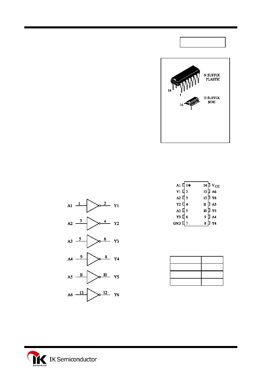
Hex Unbuffered Inverters
High-Performance Silicon-Gate CMOS
ORDERING INFORMATION
IN74HCU04AN Plastic
IN74HCU04AD SOIC
T
A
= -55
ú to 125ú C for all packages
The IN74HCU04A is identical in pinout to the 74LS04. This contain
six independent unbuffered inverters. These inverters are well suited for
use as oscillators, pulse shapers and in many other applications requiring
a high-input impedance amplifier.
This device is characterized for over wide temperature ranges to meet
industry and ation over military specifications.
û
Low Power consumption characteristic of CMOS devices
û
Output drive capability: 10 LS TTL Loads Min.
û
Operating speed superior to LS TTL
û
Wide operating voltage range: 2.0 to 6.0 V
û
Low input current: 1.0
A Max.
û
Low quiescent current: 20
A Max.
û
High noise immunity characteristic of CMOS
û
Diode protection on all inputs
PIN ASSIGNMENT
LOGIC DIAGRAM
PIN 14 =V
CC
PIN 7 = GND
FUNCTION TABLE
Inputs Output
A Y
L H
H L
1
IN74HCU04A
MAXIMUM RATINGS
*
Symbol Parameter
Value
Unit
V
CC
DC Supply Voltage (Referenced to GND)
-0.5 to +7.0
V
V
IN
DC Input Voltage (Referenced to GND)
-1.5 to V
CC
+1.5
V
V
OUT
DC Output Voltage (Referenced to GND)
-0.5 to V
CC
+0.5
V
I
IN
DC Input Current, per Pin
20
mA
I
OUT
DC Output Current, per Pin
25
mA
I
CC
DC Supply Current, V
CC
and GND Pins
50
mA
P
D
Power Dissipation in Still Air, Plastic DIP+
SOIC Package+
750
500
mW
Tstg
Storage Temperature
-65 to +150
úC
T
L
Lead Temperature, 1 mm from Case for 10 Seconds
(Plastic DIP or SOIC Package)
260
úC
*
Maximum Ratings are those values beyond which damage to the device may occur.
Functional operation should be restricted to the Recommended Operating Conditions.
+Derating - Plastic DIP: - 10 mW/
úC from 65ú to 125úC
SOIC Package: : - 7 mW/
úC from 65ú to 125úC
RECOMMENDED OPERATING CONDITIONS
Symbol Parameter Min
Max
Unit
V
CC
DC Supply Voltage (Referenced to GND)
2.0
6.0
V
V
IN
, V
OUT
DC Input Voltage, Output Voltage (Referenced to GND)
0
V
CC
V
T
A
Operating Temperature, All Package Types
-55
+125
úC
t
r
, t
f
Input Rise and Fall Time (Figure 1)
V
CC
=2.0 V
V
CC
=4.5 V
V
CC
=6.0 V
0
0
0
1000
500
400
ns
This device contains protection circuitry to guard against damage due to high static voltages or electric fields.
However, precautions must be taken to avoid applications of any voltage higher than maximum rated voltages to this
high-impedance circuit. For proper operation, V
IN
and V
OUT
should be constrained to the range GND
ò(V
IN
or
V
OUT
)
òV
CC
.
Unused inputs must always be tied to an appropriate logic voltage level (e.g., either GND or V
CC
). Unused
outputs must be left open.
2
IN74HCU04A
DC ELECTRICAL CHARACTERISTICS
(Voltages Referenced to GND)
V
CC
Guaranteed Limit
Symbol Parameter
Test
Conditions V
25
úC
to
-55
úC
ò85
úC
ò125
úC
Unit
V
IH
Minimum High-
Level Input Voltage
2.0
4.5
6.0
1.7
3.6
4.8
1.7
3.6
4.8
1.7
3.6
4.8
V
V
IL
Maximum Low -
Level Input Voltage
2.0
4.5
6.0
0.3
0.8
1.1
0.3
0.8
1.1
0.3
0.8
1.1
V
V
OH
Minimum High-
Level Output
Voltage
V
IN
=V
IH
or V
IL
I
OH
= -20
A
2.0
4.5
6.0
1.8
4.0
5.5
1.8
4.0
5.5
1.8
4.0
5.5
V
V
IN
=V
IH
or V
IL
I
OH
= -4 mA
I
OH
= -5.2 mA
4.5
6.0
3.86
5.36
3.76
5.26
3.7
5.2
V
OL
Maximum Low-
Level Output
Voltage
V
IN
=V
IH
or V
IL
I
OL
= 20
A
2.0
4.5
6.0
0.2
0.5
0.5
0.2
0.5
0.5
0.2
0.5
0.5
V
V
IN
=V
IH
or V
IL
I
OL
= 4 mA
I
OL
= 5.2 mA
4.5
6.0
0.32
0.32
0.37
0.37
0.4
0.4
I
IN
Maximum Input
Leakage Current
V
IN
=V
CC
or GND
6.0
0.1
1.0
1.0
A
I
CC
Maximum
Quiescent Supply
Current
(per Package)
V
IN
=V
CC
or GND
I
OUT
=0
A
6.0
2.0 20 40
A
3
IN74HCU04A
AC ELECTRICAL CHARACTERISTICS
(C
L
=50pF,Input t
r
=t
f
=6.0 ns)
V
CC
Guaranteed Limit
Symbol Parameter V
25
úC
to
-55
úC
ò85úC ò125úC Unit
t
PLH
, t
PHL
Maximum Propagation Delay, Input A to
Output Y (Figures 1 and 2)
2.0
4.5
6.0
80
16
14
100
20
17
120
24
20
ns
t
TLH
, t
THL
Maximum Output Transition Time, Any Output
(Figures 1 and 2)
2.0
4.5
6.0
75
15
13
95
19
16
110
22
19
ns
C
IN
Maximum Input Capacitance
-
10
10
10
pF
Power Dissipation Capacitance (Per Inverter)
Typical @25
úC,V
CC
=5.0 V
C
PD
Used to determine the no-load dynamic power
consumption:
P
D
=C
PD
V
CC
2
f+I
CC
V
CC
15 pF
tr
VCC
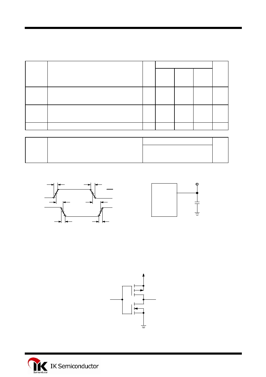
GND
90%
50%
10%
90%
50%
10%
INPUT A
OUTPUT Y
tPHL
tPLH
tTHL
tTLH
tf
* Includes all probe and jig capacitance
CL*
TEST POINT
DEVICE
UNDER
TEST
OUTPUT
Figure 1. Switching Waveforms. Figure 2. Test Circuit
LOGIC DETAIL
(1/6 of Device Show)
A
V
CC
Y
TYPICAL APPLICATIONS
4
IN74HCU04A
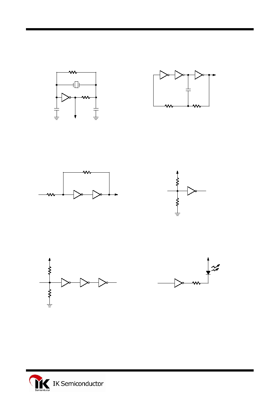
Crystal Oscillator
Stable RC Oscillator
R2
1/6 HCU04
C1
R2 > > R1
C1 < C2
Vout
C2
R1
R2
R1
C
1/6 HCU04
1/6 HCU04
1/6 HCU04
Vout
Schmitt Trigger
High Input Single-Stage Amplifier
with a 2 to 6 V Supply Range
R2
R1
Vin
Vout
1/6 HCU04 1/6 HCU04
R2 > 6R1
VCC
INPUT
OUTPUT
1 M
1 M
1/6 HCU04
Multi-Stage Amplifier
LED Driver
VCC
INPUT
OUTPUT
1/6 HCU04 1/6 HCU04 1/6 HCU04
+V
1/6 HCU04
For reduced power suplly current, use high-efficiency LEDs
such as the Hewlett-Packard HLMP series or equivalent
5