TECHNICAL DATA
1
Hex Inverters
with Open-Drain Outputs
This device contains idenpendent inverts. It performs the Boolean
function Y=A. The open collector outputs require pull-up resistor to
perform correctly. Open-collector devices are often used to generate
higher V
OH
levels.
Pull-Up Resistor Equations
R
MAX
=
R
MIN
=
Where: N
1
(I
OH
)=total maximumoutput high current for all outputs tied
to pull-up resistor
N
2
(I
IH
)=total input high current for all inputs tied to pull-up
resistor
N
3
(I
IL
)=total input low current for all inputs tied to pull-up
resistor
IN74LS05
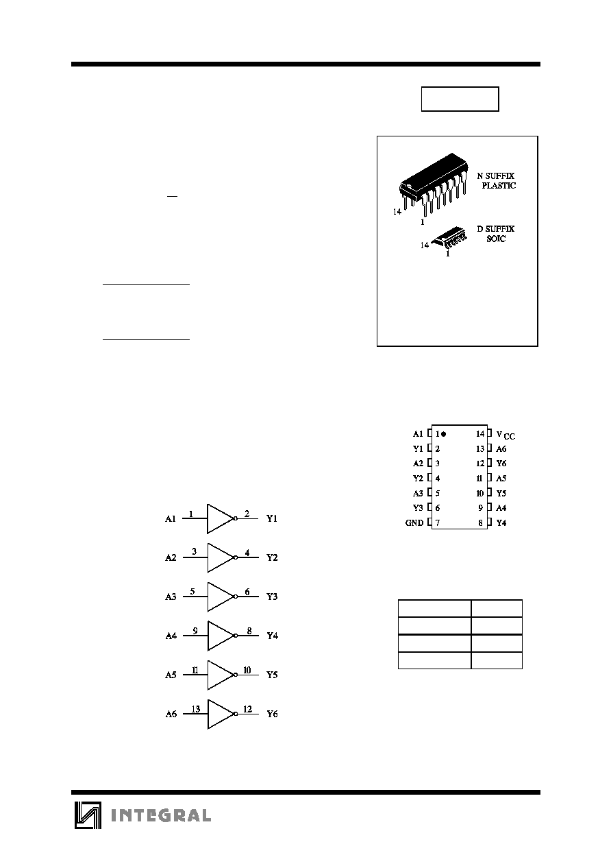
ORDERING INFORMATION
IN74LS05N Plastic
IN74LS05D SOIC
T
A
= -0
ú
to 70
ú
C
for all packages
LOGIC DIAGRAM
PIN 14 =V
CC
PIN 7 = GND
PIN ASSIGNMENT
FUNCTION TABLE
Inputs
Output
A
Y
L
H
H
L
V
CC
(Min) - V
OH
V
CC
(Max) - V
OL
N
1
(I
OH
) + N
2
(I
IH
)
(I
OL
+ N
3
(I
IL
)

IN74LS05
2
MAXIMUM RATINGS
*
Symbol
Parameter
Value
Unit
V
CC
Supply Voltage
7.0
V
V
IN
Input Voltage
7.0
V
V
OUT
Output Voltage
7.0
V
Tstg
Storage Temperature Range
-65 to +150
ú
C
*
Maximum Ratings are those values beyond which damage to the device may occur.
Functional operation should be restricted to the Recommended Operating Conditions.
RECOMMENDED OPERATING CONDITIONS
Symbol
Parameter
Min
Max
Unit
V
CC
Supply Voltage
4.75
5.25
V
V
IH
High Level Input Voltage
2.0
V
V
IL
Low Level Input Voltage
0.8
V
V
OH
High Level Output Voltage
5.5
V
I
OL
Low Level Output Current
8.0
mA
T
A
Ambient Temperature Range
0
+70
ú
C
DC ELECTRICAL CHARACTERISTICS over full operating conditions
Guaranteed Limit
Symbol
Parameter
Test Conditions
Min
Max
Unit
V
IK
Input Clamp Voltage
V
CC
= min, I
IN
= -18 mA
-1.5
V
I
OH
High Level Output Current
V
CC
= min, V
OH
=max
0.1
mA
V
OL
Low Level Output Voltage
V
CC
= min, I
OL
= 4 mA
0.4
V
V
CC
= min, I
OL
= 8 mA
0.5
I
IH
High Level Input Current
V
CC
= max, V
IN
= 2.7 V
20
A
V
CC
= max, V
IN
= 7.0 V
0.1
mA
I
IL
Low Level Input Current
V
CC
= max, V
IN
= 0.4 V
-0.4
mA
I
CC
Supply Current
V
CC
= max
Total with
outputs high
2.4
mA
Total with
outputs low
6.6

IN74LS05
3
AC ELECTRICAL CHARACTERISTICS
(V
CC
= 5.0 V, C
L
= 15 pF, T
A
=25
ú
C, R
L
= 2 k
, t
r
=15
ns, t
f
= 6.0 ns)
Symbol
Parameter
Min
Max
Unit
t
PLH
Propagation Delay Time
32
ns
t
PHL
Propagation Delay Time
28
ns
Figure 1. Switching Waveforms
NOTE A. C
L
includes probe and jig capacitance.
Figure 2. Test Circuit