 | –≠–ª–µ–∫—Ç—Ä–æ–Ω–Ω—ã–π –∫–æ–º–ø–æ–Ω–µ–Ω—Ç: IN74LS164 | –°–∫–∞—á–∞—Ç—å:  PDF PDF  ZIP ZIP |
TECHNICAL DATA
1
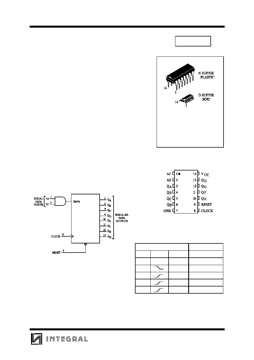
8-Bit Serial-Input/Parallel-Output
Shift Register
This 8-bit shift register features gated serial inputs and an
asynchronous reset. The gated serial inputs (A and B) permit complete
control over incoming data as a low at either (or both) input(s) inhibits
entry of the new data and resets the first flip flop to the low level at the
next clock pulse. A high level input enables the other input which will
then determine the state of the first flip-flop. Data at the serial inputs
may be changed while the clock is high or low, but only information
meeting the setup requirements will be entered clocking occurs or the
low-to-high level transition of the clock input. All inputs are diode-
clamped to minimize transmission-line effects.
û
Gated (Enable/Disable) Serial Inputs
û
Fully Buffered Clock and Serial Inputs
û
Asynchronous Clear
IN74LS164
ORDERING INFORMATION
IN74LS164N Plastic
IN74LS164D SOIC
T
A
=0
ú
to 70
ú
C
for all packages
PIN ASSIGNMENT
FUNCTION TABLE
Inputs
Outputs
Reset
Clock
A1 A2
Q
A
Q
B
... Q
H
L
X
X X
L L ... L
H
X X
no change
H
H D
D Q
An
... Q
Gn
H
D H
D Q
An
... Q
Gn
H
L L
L Q
An
... Q
Gn
D = data input
X = don't care
Q
An
- Q
Gn
= data shifted from the previous stage on a
rising edge at the clock input.
LOGIC DIAGRAM
PIN 14 =V
CC
PIN 7 = GND
IN74LS164
2
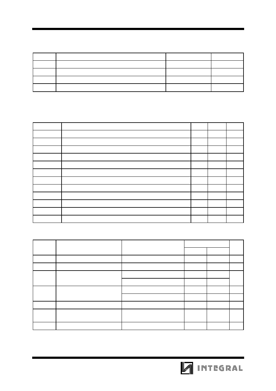
MAXIMUM RATINGS
*
Symbol
Parameter
Value
Unit
V
CC
Supply Voltage
7.0
V
V
IN
Input Voltage
7.0
V
V
OUT
Output Voltage
5.5
V
Tstg
Storage Temperature Range
-65 to +150
ú
C
*
Maximum Ratings are those values beyond which damage to the device may occur.
Functional operation should be restricted to the Recommended Operating Conditions.
RECOMMENDED OPERATING CONDITIONS
Symbol
Parameter
Min
Max
Unit
V
CC
Supply Voltage
4.75
5.25
V
V
IH
High Level Input Voltage
2.0
V
V
IL
Low Level Input Voltage
0.8
V
I
OH
High Level Output Current
-0.4
mA
I
OL
Low Level Output Current
8.0
mA
T
A
Ambient Temperature Range
0
+70
ú
C
f
clock
Clock Frequency
0
25
MHz
t
su
Setup Time, A1 or A2 to Clock
15
ns
t
h
Hold Time, Clock to A1 or A2
5
ns
t
w
Pulse Width, Clock
20
ns
t
w
Pulse Width, Reset
20
ns
t
rec
Recovery Time
5
ns
DC ELECTRICAL CHARACTERISTICS over full operating conditions
Guaranteed Limit
Symbol
Parameter
Test Conditions
Min
Max
Unit
V
IK
Input Clamp Voltage
V
CC
= min, I
IN
= -18 mA
-1.5
V
V
OH
High Level Output Voltage
V
CC
= min, I
OH
= -0.4 mA
2.7
V
V
OL
Low Level Output Voltage
V
CC
= min, I
OL
= 4 mA
0.4
V
V
CC
= min, I
OL
= 8 mA
0.5
I
IH
High Level Input Current
V
CC
= max, V
IN
= 2.7 V
20
mA
V
CC
= max, V
IN
= 7.0 V
0.1
mA
I
IL
Low Level Input Current
V
CC
= max, V
IN
= 0.4 V
-0.4
mA
I
O
Output Short Circuit Current
V
CC
= max, V
O
= 0 V
(Noote 1)
-20
-100
mA
I
CC
Supply Current
V
CC
= max (Note 2)
27
mA
Note 1: Not more than one output should be shorted at a time, and duration should not exceed one second.
Note 2: I
CC
is measured with outputs open, serial inputs grouned, the clock input at 2.4 V, and a momentary
ground, then 4.5 V applied.

IN74LS164
3
AC ELECTRICAL CHARACTERISTICS
(T
A
=25
ú
C, V
CC
= 5.0 V, C
L
= 15 pF, R
L
= 2 k
, t
r
=15
ns, t
f
= 6.0 ns)
Symbol
Parameter
Min
Max
Unit
t
PLH
Propagation Delay Time, Clock to Q
27
ns
t
PHL
Propagation Delay Time, Clock to Q
32
ns
t
PHL
Propagation Delay Time, Reset to Q
36
ns
t
su
Setup Time, A1 or A2 to Clock
15
ns
t
h
Hold Time, Clock to A1 or A2
5
ns
t
w
Pulse Width, Clock
20
ns
t
w
Pulse Width, Reset
20
ns
Figure 1. Switching Waveforms
Figure 2. Switching Waveforms
NOTES A. C
L
includes probe and jig capacitance.
B. All diodes are 1N916 or 1N3064.
Figure 3. Switching Waveform
Figure 4. Test Circuit
IN74LS164
4
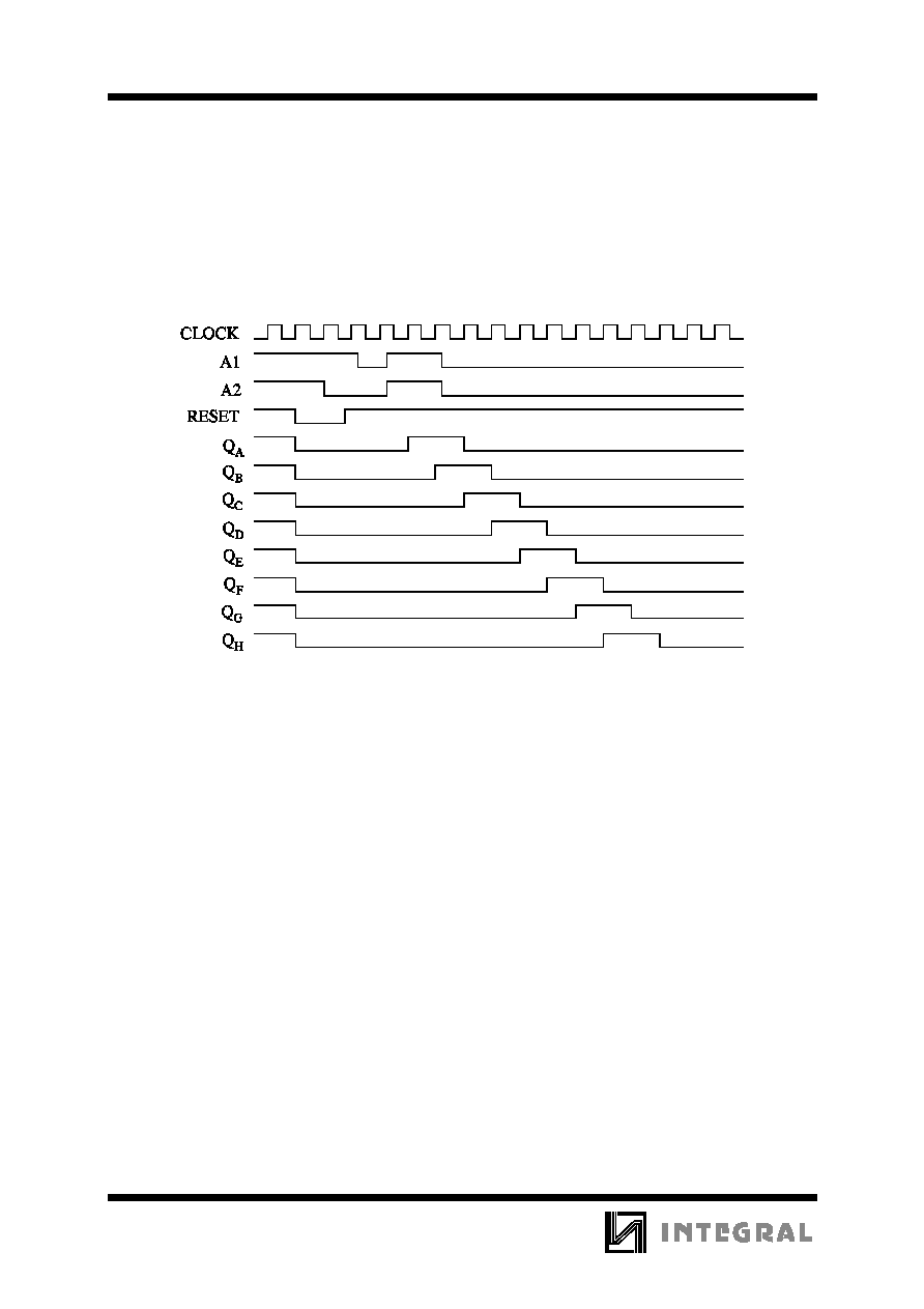
TIMING DIAGRAM