 | –≠–ª–µ–∫—Ç—Ä–æ–Ω–Ω—ã–π –∫–æ–º–ø–æ–Ω–µ–Ω—Ç: IN74LV164 | –°–∫–∞—á–∞—Ç—å:  PDF PDF  ZIP ZIP |

TECHNICAL DATA
1
INTEGRAL
8-BIT SERIAL-IN/PARALLEL-OUT SHIFT REGISTER
The IN74LV164 is a low-voltage Si-gate CMOS device and is pin
and function compatible with the IN74HC/HCT164.
The IN74LV164 is an 8-bit edge-triggered shift register with serial
data entry and an output from each of the eight stages. Data is entered
serially through one of two inputs (DSA or DSB); either input can be
used as an active HIGH enable for data entry through the other input.
Both inputs must be connected together or an unused input must be tied
HIGH.
Data shifts one place to the right on each LOW-to-HIGH transition
of the clock (CP) input and enters into Q
0
, which is the logical AND of
the two data inputs (DSA, DSB ) that existed one set-up time prior to the
rising clock edge.
A LOW on the master reset (MR) input overrides all other inputs
and clears the register asynchronously, forcing all outputs LOW.
û
Outputs Directly Interface to CMOS, NMOS, and TTL
û
Operating Voltage Range: 1.2 to 5.5 V
û
Low Input Current: 1.0
A, 0.1
at = 25
ú
û
Output Current: 6 mA at V
CC
= 3.0 V; 12 mA at V
CC
= 4.5 V
û
High Noise Immunity Characteristic of CMOS Devices
IN74LV164
1
14
1
14
N SUFFIX
PLASTIC DIP
D SUFFIX
SO
ORDERING INFORMATION
IN74LV164N
Plastic DIP
IN74LV164D
SOIC
IZ74LV164
chip
T
A
= -40
ú
to 125
ú
C for all packages
LOGIC DIAGRAM
PIN 14=V
CC
PIN 7 = GND
PIN ASSIGNMENT
FUNCTION TABLE
Inputs
Outputs
MR
CP
DSA DSB Q0 Q1 ... Q7
L
X
X
X
L
L ... L
H
L
L
L
Q0 ... Q6
H
L
H
L
Q0 ... Q6
H
H
L
L
Q0 ... Q6
H
H
H
H
Q0 ... Q6
H = high voltage level
L = low voltage level
X = don't care
1
2
3
5
4
6
7
V
CC
14
13
12
11
10
8
9
GND
DSA
DSB
Q0
Q1
Q2
Q3
Q7
Q6
Q5
Q4
MR
CP
DSA
DSB
CP
SERIAL
DATA
INPUTS
PARALLEL
DATA
OUTPUTS
MR
Q0
Q4
Q2
Q6
Q1
Q5
Q3
Q7
1
2
8
9
2
10
5
12
4
11
6
13
DATA

IN74LV164
2
INTEGRAL
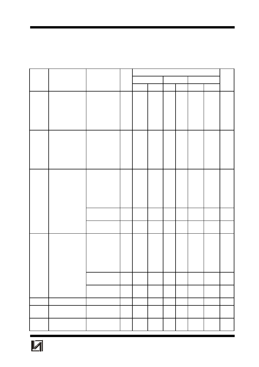
MAXIMUM RATINGS
*
Symbol
Parameter
Value
Unit
V
CC
DC supply voltage
-0.5 to + 7.0
V
I
IK
*
1
DC Input diode current
20
mA
I
OK
*
2
DC Output diode current
50
mA
I
O
*
3
DC Output source or sink current
25
mA
I
CC
V
CC
current
50
mA
I
GND
GND current
50
mA
P
D
Power dissipation per package: *
4
Plastic DIP
SO
750
500
mW
Tstg
Storage Temperature
-65 to +150
ú
C
T
L
Lead Temperature, 1.5 mm (Plastic DIP Package), 0.3 mm (SO
Package) from Case for 4 Seconds
260
ú
C
*
Maximum Ratings are those values beyond which damage to the device may occur.
Functional operation should be restricted to the Recommended Operating Conditions.
*
1
V
I
< -0.5 V or V
I
> V
CC
+ 0.5 V.
*
2
V
O
< -0.5 V or V
O
> V
CC
+ 0.5 V.
*
3
-0.5 V < V
O
< V
CC
+ 0.5 V.
*
4
Derating - Plastic DIP: - 12 mW/
ú
C from 70
ú
to 125
ú
C
SO Package: : - 8 mW/
ú
C from 70
ú
to 125
ú
C
RECOMMENDED OPERATING CONDITIONS
Symbol
Parameter
Min
Max
Unit
V
CC
DC Supply Voltage
1.2
5.5
V
V
I
Input Voltage
0
V
CC
V
V
O
Output Voltage
0
V
CC
V
T
A
Operating Temperature, All Package Types
-40
+125
ú
C
t
r
, t
f
Input Rise and Fall Time (Figure 1)
1.0 V
ò
V
CC
< 2.0 V
2.0 V
ò
V
CC
< 2.7 V
2.7 V
ò
V
CC
< 3.6 V
3.6 V
ò
V
CC
ò
5.5 V
0
0
0
0
500
200
100
50
ns
This device contains protection circuitry to guard against damage due to high static voltages or electric
fields. However, precautions must be taken to avoid applications of any voltage higher than maximum rated voltages
to this high-impedance circuit. For proper operation, V
IN
and V
OUT
should be constrained to the range GND
ò
(V
IN
or
V
OUT
)
ò
V
CC
.
Unused inputs must always be tied to an appropriate logic voltage level (e.g., either GND or V
CC
). Unused
outputs must be left open.
IN74LV164
3
INTEGRAL
DC ELECTRICAL CHARACTERISTICS
(Voltages Referenced to GND)
Test
V
CC
Guaranteed Limit
Symbol
Parameter
conditions
V
25
ú
C to -40
ú
C
85
ú
C
125
ú
C
Unit
min
max
min
max
min
max
V
IH
HIGH level input
voltage
1.2
2.0
2.7
3.0
3.6
4.5
5.5
0.9
1.4
2.0
2.0
2.0
3.15
3.85
-
-
-
-
-
-
-
0.9
1.4
2.0
2.0
2.0
3.15
3.85
-
-
-
-
-
-
-
0.9
1.4
2.0
2.0
2.0
3.15
3.85
-
-
-
-
-
-
-
V
V
IL
LOW level input
voltage
1.2
2.0
2.7
3.0
3.6
4.5
5.5
-
-
-
-
-
-
-
0.3
0.6
0.8
0.8
0.8
1.35
1.65
-
-
-
-
-
-
-
0.3
0.6
0.8
0.8
0.8
1.35
1.65
-
-
-
-
-
-
-
0.3
0.6
0.8
0.8
0.8
1.35
1.65
V
V
OH
HIGH level output
voltage
V
I
= V
IH
or V
IL
I
O
= -100
1.2
2.0
2.7
3.0
3.6
4.5
5.5
1.05
1.85
2.55
2.85
3.45
4.35
5.35
-
-
-
-
-
-
-
1.0
1.8
2.5
2.8
3.4
4.3
5.3
-
-
-
-
-
-
-
1.0
1.8
2.5
2.8
3.4
4.3
5.3
-
-
-
-
-
-
-
V
V
I
= V
IH
or V
IL
I
O
= -6.0 m
3.0
2.48
-
2.40
-
2.20
-
V
V
I
= V
IH
or V
IL
I
O
= -12.0 m
4.5
3.70
-
3.60
-
3.50
-
V
V
OL
LOW level output
voltage
V
I
= V
IH
or V
IL
I
O
= 100
1.2
2.0
2.7
3.0
3.6
4.5
5.5
-
-
-
-
-
-
-
0.15
0.15
0.15
0.15
0.15
0.15
0.15
-
-
-
-
-
-
-
0.2
0.2
0.2
0.2
0.2
0.2
0.2
-
-
-
-
-
-
-
0.2
0.2
0.2
0.2
0.2
0.2
0.2
V
V
I
= V
IH
or V
IL
I
O
= 6.0 m
3.0
-
0.33
-
0.4
-
0.5
V
V
I
= V
IH
or V
IL
I
O
= 12.0 m
4.5
-
0.40
-
0.55
-
0.65
V
I
I
Input current
V
I
= V
CC
or 0 V
5.5
-
0.1
-
1.0
-
1.0
I
CC
Supply current
V
I
=V
CC
or 0 V
I
O
= 0
5.5
-
8.0
-
80
-
160
I
CC1
Supply current
V
I
=V
CC
- 0.6 V
2.7
3.6
-
0.2
-
0.5
-
0.85
m

IN74LV164
4
INTEGRAL
AC ELECTRICAL CHARACTERISTICS
(C
L
=50 pF, t
r
=t
f
= 2.5 ns, R
L
= 1 k
)
Test
V
CC
Guaranteed Limit
Symbol
Parameter
conditions
V
25
ú
C to -40
ú
C
85
ú
C
125
ú
C
Unit
min
max
min
max
min
max
t
PHL,
t
PLH
Propagation delay , CP to
Qn
V
I
= 0 V or V
1
Figure 1 and 4
1.2
2.0
2.7
3.0
4.5
-
-
-
-
-
150
30
23
18
15
-
-
-
-
-
180
39
29
23
19
-
-
-
-
-
210
49
36
29
24
ns
t
PHL
Propagation delay , MR to
Qn
V
I
= 0 V or V
1
Figure 1 and 4
1.2
2.0
2.7
3.0
4.5
-
-
-
-
-
150
30
23
18
15
-
-
-
-
-
180
39
29
23
19
-
-
-
-
-
210
49
36
29
24
ns
t
w
Pulse Width, CP or MR
V
I
= 0 V or V
1
Figure 1
1.2
2.0
2.7
3.0
4.5
100
28
21
17
14
-
-
-
-
-
130
34
25
20
17
-
-
-
-
-
160
41
30
24
20
-
-
-
-
-
ns
t
su
Setup Time, DSA or DSB
to CP
V
I
= 0 V or V
1
Figure 3
1.2
2.0
2.7
3.0
4.5
60
19
13
11
9
-
-
-
-
-
80
22
16
13
11
-
-
-
-
-
100
26
19
15
13
-
-
-
-
-
ns
t
h
Hold Time, DSA or DSB to
CP
V
I
= 0 V or V
1
Figure 3
1.2
2.0
2.7
3.0
4.5
50
5
5
5
5
-
-
-
-
-
50
5
5
5
5
-
-
-
-
-
50
5
5
5
5
-
-
-
-
-
ns
t
rec
Recovery Time, MR to CP V
I
= 0 V or V
1
Figure 2
1.2
2.0
2.7
3.0
4.5
70
15
11
9
8
-
-
-
-
-
100
19
14
11
10
-
-
-
-
-
130
24
18
14
12
-
-
-
-
-
ns
f
max
Clock Frequency
V
I
= 0 V or V
1
Figure 1 and 4
1.2
2.0
2.7
3.0
4.5
-
-
-
-
-
2
16
22
27
32
-
-
-
-
-
1
14
19
24
27
-
-
-
-
-
1
12
16
20
24
MHz
C
I
Input capacitance
5.0
-
7.0
-
-
-
-
pF
C
PD
Power dissipation
capacitance
V
I
= 0 V or V
CC
5.5
-
80
-
-
-
-
pF
IN74LV164
5
INTEGRAL
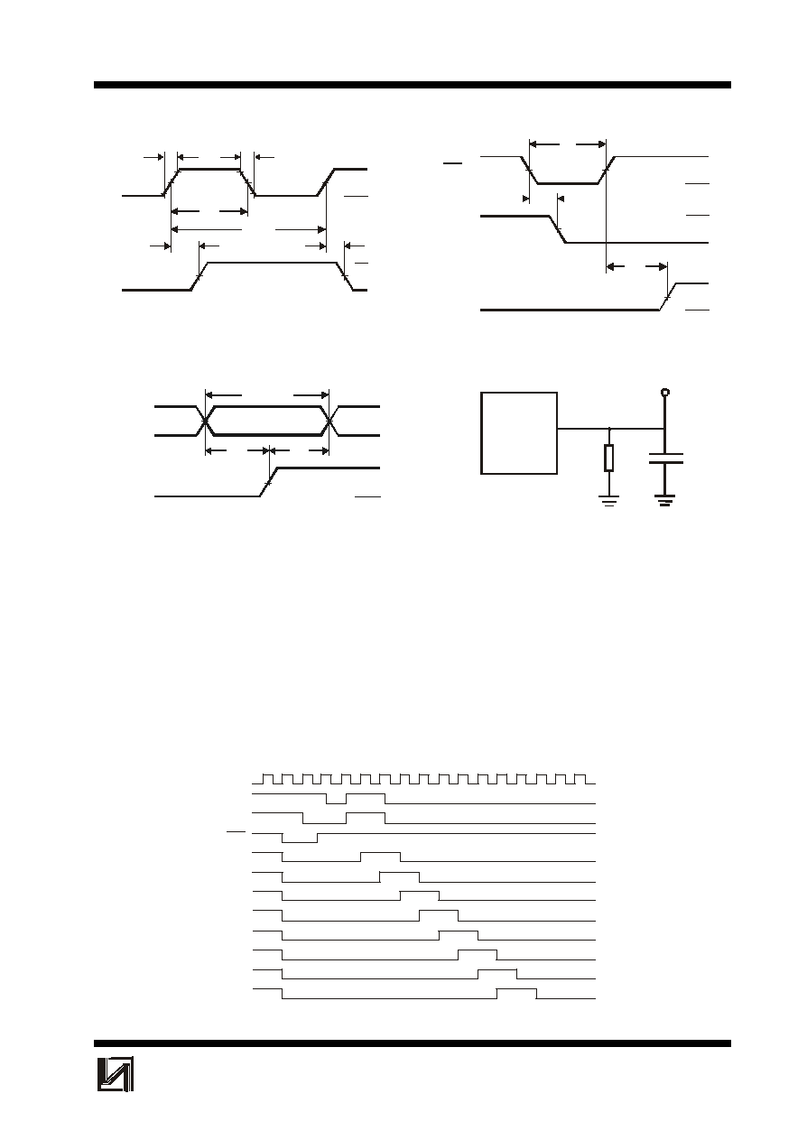
Figure 1. Switching Waveforms
Figure 2. Switching Waveforms
* Includes all probe and jig capacitance
Figure 3. Switching Waveforms
Figure 4. Test Circuit
Note:
(1)
V
M
= 1.5 V at V
CC
= 2.7 V
V
M
= 0.5
V
CC
at V
CC
=1.2 V, 2.0 V, 3.0 V, 4.5 V
(2)
V
1
= V
CC
at V
CC
=1.2 V, 2.0 V, 2.7 V, 4.5 V
V
1
= 2.7 V at V
CC
= 3.0 V
TIMING DIAGRAM
GND
90%
V
M
(1 )
V
M
(1)
V
M
(1)
V
M
( 1)
V
M
(1 )
V
1
(2)
V
OH
V
OH
V
1
(2)
V
1
(2)
10%
t
t
t
t
f
r
PLH
PHL
t
w
1/fmax
CP
Q
MR
Q
t
PHL
GND
GND
t
rec
CP
t
w
V
OL
V
OL
DEVICE
UNDER
TEST
OUTPUT
C
L
*
R
L
TEST POINT
V
M
(1 )
V
M
( 1)
t
GND
GND
t
su
h
VALID
DSA or DSB
CP
V
1
(2)
V
1
(2)
CP
DSA
DSB
MR
Q0
Q1
Q2
Q3
Q4
Q5
Q6
Q7