TECHNICAL DATA
1
INTEGRAL
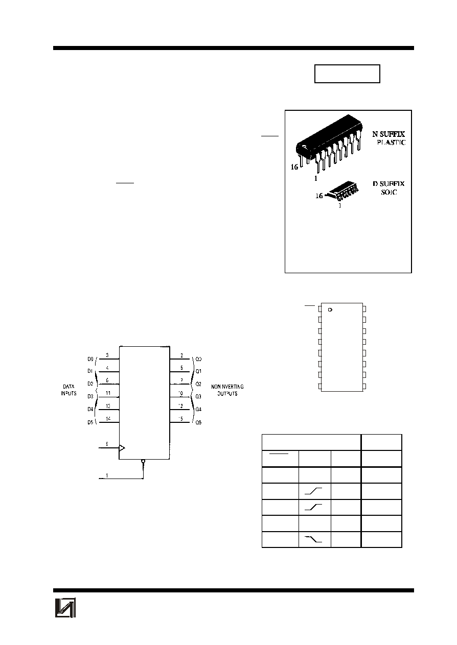
Hex D-type flip-flop with reset; positive edge-trigger
The 74LV174 is a low-voltage Si-gate CMOS device and is pin and
function compatible with the 74HC/HCT174.
The 74LV174 has six edge-triggered D-type flip-flops with individual D
inputs and Q outputs. The common clock (CP) and master reset (MR)
inputs load and reset (clear) all flip-flops simultaneously.
The register is fully edge-triggered. The state of each D input, one set-
up time prior to the LOW-to-HIGH clock transition, is transferred to the
corresponding output of the flip-flop.
A LOW level on the MR input forces all outputs LOW, independently of
clock or data inputs.
The device is useful for applications requiring true outputs only and
clock and master reset inputs that are common to all storage elements.
û
Output voltage levels are compatible with input levels of CMOS,
NMOS and TTL IC
S
û
Supply voltage range: 1.2 to 5.5 V
û
Low input current: 1.0
; 0.1
at = 25
ú
û
Output current: 6 mA at Vcc = 3.0 V; 12 mA at Vcc = 4.5 V
û
High Noise Immunity Characteristic of CMOS Devices
IN74LV174
ORDERING INFORMATION
IN74LV174N Plastic
IN74LV174D SOIC
IZ74LV174 Chip
T
A
= -40
ú
to 125
ú
C for all packages
FUNCTION TABLE
Inputs
Outputs
MR
CP
Dn
Qn
L
X
X
L
H
H
H
H
L
L
H
L
X
no change
H
X
no change
H= high level
L = low level
X = don't care
LOGIC DIAGRAM
PIN 16=V
CC
PIN 08 = GND
PIN ASSIGNMENT
1
2
3
5
4
6
7
8
GND
16
15
14
13
12
11
10
9
V CC
MR
Q0
D0
D1
Q1
D2
Q2
D5
D4
Q4
D3
Q3
CP
Q5
MR
CP

IN74LV174
2
INTEGRAL
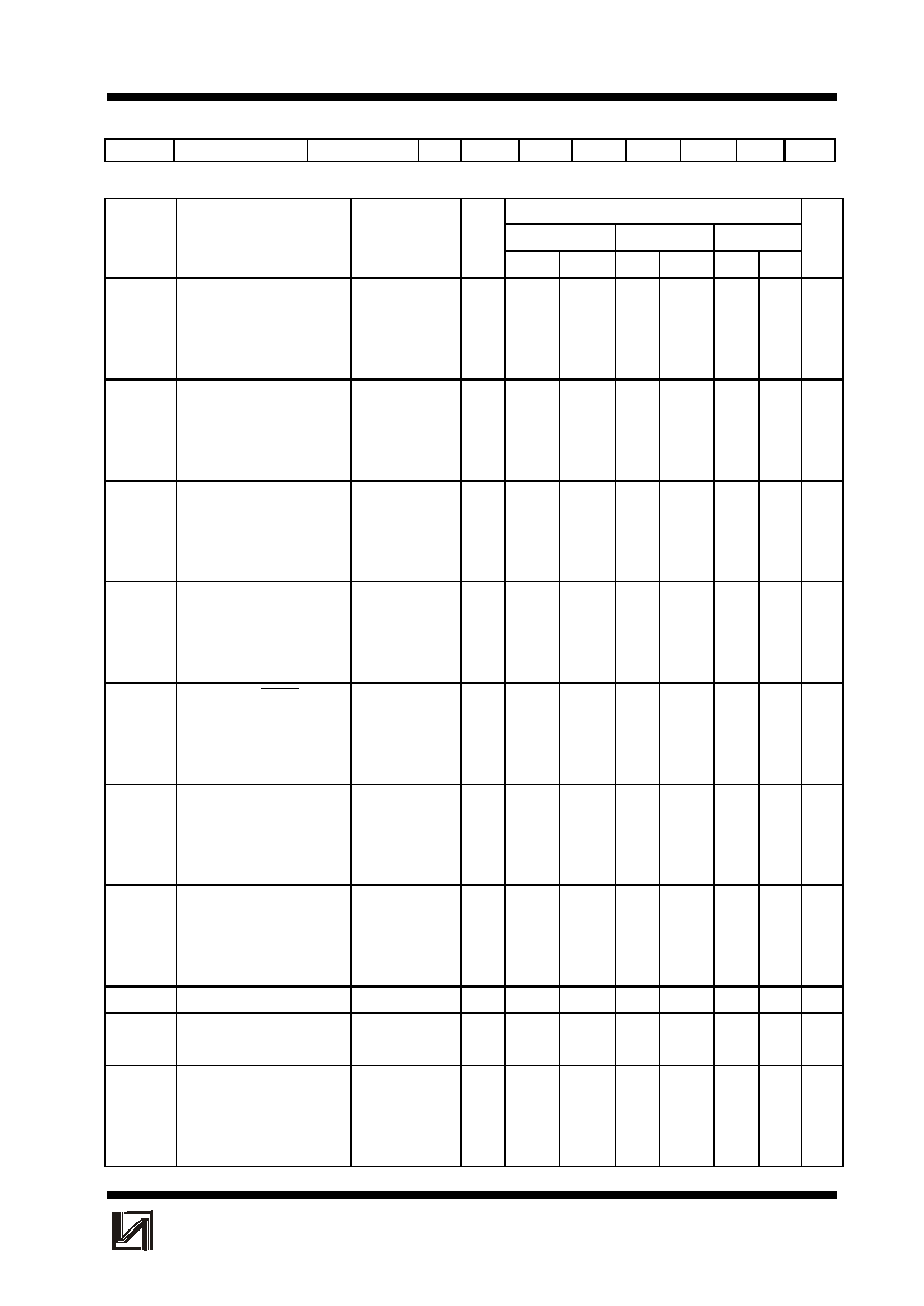
MAXIMUM RATINGS
*
Symbol
Parameter
Value
Unit
V
CC
DC supply voltage
-0.5 to +5.0
V
I
IK
*
1
Input diode current
20
mA
I
OK
*
2
Output diode current
50
mA
I
O
*
3
Output source or sink current
25
mA
I
CC
V
CC
current
50
mA
I
GND
GND current
50
mA
P
D
Power dissipation per package: *
4
Plastic DIP
SO
750
500
mW
Tstg
Storage Temperature
-65 to +150
ú
C
T
L
Lead Temperature, 1.5 mm (Plastic DIP Package), 0.3 mm (SO
Package) from Case for 4 Seconds
260
ú
C
*
Maximum Ratings are those values beyond which damage to the device may occur.
Functional operation should be restricted to the Recommended Operating Conditions.
*
1
V
I
< -0.5 V or V
I
> V
CC
+ 0.5 V
*
2
V
O
< -0.5 V or V
O
> V
CC
+ 0.5 V
*
3
-0.5 V < V
O
< V
CC
+ 0.5 V
*
4
Derating - Plastic DIP: - 12 mW/
ú
C from 70
ú
to 125
ú
C
SO Package: : - 8 mW/
ú
C from 70
ú
to 125
ú
C
RECOMMENDED OPERATING CONDITIONS
Symbol
Parameter
Min
Max
Unit
V
CC
DC Supply Voltage
1.2
5.5
V
V
IN
DC Input Voltage
0
V
CC
V
V
OUT
DC Output Voltage
0
V
CC
V
T
A
Operating Temperature, All Package Types
-40
+125
ú
C
t
r
, t
f
Input Rise and Fall Time (Figure 1)
1.0
ò
V
CC
<
2.0
2.0
ò
V
CC
<
2.7
2.7
ò
V
CC
<
3.6
3.6
ò
V
CC
ò
5.5
0
0
0
0
500
200
100
50
ns/V
This device contains protection circuitry to guard against damage due to high static voltages or electric
fields. However, precautions must be taken to avoid applications of any voltage higher than maximum rated voltages
to this high-impedance circuit. For proper operation, V
IN
and V
OUT
should be constrained to the range GND
ò
(V
IN
or
V
OUT
)
ò
V
CC
.
Unused inputs must always be tied to an appropriate logic voltage level (e.g., either GND or V
CC
). Unused
outputs must be left open.

IN74LV174
3
INTEGRAL
DC ELECTRICAL CHARACTERISTICS
(Voltages Referenced to GND)
Test
V
CC
Guaranteed Limit
Symbol
Parameter
conditions
V
-40
ú
C to 25
ú
C
85
ú
C
125
ú
C
Unit
min
max
min
max
min
max
V
IH
HIGH level input
voltage
1.2
2.0
2.7
3.0
3.6
4.5
5.5
0.9
1.4
2.0
2.0
2.0
3.15
3.85
-
-
-
-
-
-
-
0.9
1.4
2.0
2.0
2.0
3.15
3.85
-
-
-
-
-
-
-
0.9
1.4
2.0
2.0
2.0
3.15
3.85
-
-
-
-
-
-
-
V
V
IL
LOW level input
voltage
1.2
2.0
2.7
3.0
3.6
4.5
5.5
-
-
-
-
-
-
-
0.3
0.6
0.8
0.8
0.8
1.35
1.65
-
-
-
-
-
-
-
0.3
0.6
0.8
0.8
0.8
1.35
1.65
-
-
-
-
-
-
-
0.3
0.6
0.8
0.8
0.8
1.35
1.65
V
V
OH
HIGH level output
voltage
V
I
= V
IH
or V
IL
I
O
= -100
1.2
2.0
2.7
3.0
3.6
4.5
5.5
1.05
1.85
2.55
2.85
3.45
4.35
5.35
-
-
-
-
-
-
-
1.0
1.8
2.5
2.8
3.4
4.3
5.3
-
-
-
-
-
-
-
1.0
1.8
2.5
2.8
3.4
4.3
5.3
-
-
-
-
-
-
-
V
V
I
= V
IH
or V
IL
I
O
= -6 m
3.0
2.48
-
2.34
-
2.20
-
V
V
I
= V
IH
or V
IL
I
O
= -12 m
4.5
3.70
-
3.60
-
3.50
-
V
V
OL
LOW level output
voltage
V
I
= V
IH
or V
IL
I
O
= 100
1.2
2.0
2.7
3.0
3.6
4.5
5.5
-
-
-
-
-
-
-
0.15
0.15
0.15
0.15
0.15
0.15
0.15
-
-
-
-
-
-
-
0.2
0.2
0.2
0.2
0.2
0.2
0.2
-
-
-
-
-
-
-
0.2
0.2
0.2
0.2
0.2
0.2
0.2
V
V
I
= V
IH
or V
IL
I
O
= 6 m
3.0
-
0.33
-
0.40
-
0.50
V
V
I
= V
IH
or V
IL
I
O
= 12 m
4.5
-
0.40
-
0.55
-
0.65
V
I
I
Input current
V
I
= V
CC
or 0 V
5.5
-
0.1
-
1.0
-
1.0
I
CC
Supply current
V
I
=V
CC
or 0 V
I
O
= 0
5.5
-
8.0
-
80
-
160
I
CC1
Additional
quiescent supply
current per input
V
I
=V
CC
- 0.6 V
2.7
3.6
-
0.2
0.2
-
0.5
0.5
-
0.85
0.85
mA
IN74LV174
4
INTEGRAL
current per input
AC ELECTRICAL CHARACTERISTICS
(C
L
=50 pF, R
L
= 1 k
, t
r
=t
f
=2.5 ns)
Test
V
CC
Guaranteed Limit
Symbol
Parameter
conditions
V
-40
ú
C to 25
ú
C
85
ú
C
125
ú
C
Unit
min
max
min
max
min
max
t
PHL,
t
PLH
Propagation delay CP to
Qn
V
I
= 0 V or V
CC
Figure 1, 4
1.2
2.0
2.7
3.0
4.5
-
-
-
-
-
200
34
24
20
17
-
-
-
-
-
230
43
31
25
21
-
-
-
-
-
260
53
39
31
26
ns
t
PHL
Propagation delay MR to
Qn
V
I
= 0 V or V
CC
Figure 2, 4
1.2
2.0
2.7
3.0
4.5
-
-
-
-
-
160
34
24
20
17
-
-
-
-
-
190
43
31
25
21
-
-
-
-
-
220
53
39
31
26
ns
t
W
Clock pulse width HIGH or
LOW
V
I
= 0 V or V
CC
Figure 1, 4
1.2
2.0
2.7
3.0
4.5
100
28
21
17
14
-
-
-
-
-
140
34
25
20
17
-
-
-
-
-
180
41
30
24
20
-
-
-
-
-
ns
t
W
Master reset pulse width
LOW
V
I
= 0 V or V
CC
Figure 1, 4
1.2
2.0
2.7
3.0
4.5
100
28
21
17
14
-
-
-
-
-
140
34
25
20
17
-
-
-
-
-
180
41
30
24
20
-
-
-
-
-
ns
t
REM
Removal time MR to CP
V
I
= 0 V or V
CC
Figure 3, 4
1.2
2.0
2.7
3.0
4.5
40
19
13
11
9
-
-
-
-
-
60
22
16
13
11
-
-
-
-
-
80
26
19
15
13
-
-
-
-
-
ns
t
SU
Set-up time Dn to CP
V
I
= 0 or V
CC
3, 4
1.2
2.0
2.7
3.0
4.5
50
5
5
5
5
-
-
-
-
-
50
5
5
5
5
-
-
-
-
-
50
5
5
5
5
-
-
-
-
-
ns
t
h
Hold time Dn to CP
V
I
= 0 or V
CC
2, 4
1.2
2.0
2.7
3.0
4.5
50
5
5
5
5
-
-
-
-
-
50
5
5
5
5
-
-
-
-
-
50
5
5
5
5
-
-
-
-
-
ns
C
I
Input capacitance
A
= 25
ú
C
5.0
-
7.0
-
-
-
-
pF
C
PD
Power dissipation
capacitance (per flip-flop)
V
I
= 0 V or V
CC
T
A
= 25
ú
C
5.5
-
34
-
-
-
-
pF
fmax
Maximum clock pulse
frequency
V
I
= 0 or V
CC
1
1.2
2.0
2.7
3.0
4.5
-
-
-
-
-
2.0
16
22
27
32
-
-
-
-
-
1.0
14
19
24
27
-
-
-
-
-
1.0
12
16
20
24
MHz
IN74LV174
5
INTEGRAL
Figure 1. Switching Waveforms
Figure 2. Switching Waveforms
* Includes all probe and jig capacitance
Figure 3. Switching Waveforms
Figure 4. Test Circuit
Note:
(1)
V
M
= 1.5 V at V
CC
= 2.7 V
V
M
= 0.5
V
CC
at V
CC
=1.2 V, 2.0 V, 3.0 V, 4.5 V
(2)
V
1
= V
CC
at V
CC
=1.2 V, 2.0 V, 2.7 V, 4.5 V
V
1
= 2.7 V at V
CC
= 3.0 V
GND
90%
V
M
(1 )
V
M
(1)
V
M
(1)
V
M
( 1)
V
M
(1 )
V
1
(2)
V
OH
V
OH
V
1
(2)
V
1
(2)
10%
t
t
t
t
f
r
PLH
PHL
t
w
1/fmax
CP
Q
MR
Q
t
PHL
GND
GND
t
rec
CP
t
w
V
OL
V
OL
DEVICE
UNDER
TEST
OUTPUT
C
L
*
R
L
TEST POINT
V
M
(1 )
V
M
( 1)
t
GND
GND
t
su
h
VALID
DATA
CP
V
1
(2)
V
1
(2)