 | –≠–ª–µ–∫—Ç—Ä–æ–Ω–Ω—ã–π –∫–æ–º–ø–æ–Ω–µ–Ω—Ç: IN74LVU04 | –°–∫–∞—á–∞—Ç—å:  PDF PDF  ZIP ZIP |
IN74LVU04
1
H
EX
I
NVERTER
The 74LVU04 is a low-voltage, Si-gate CMOS device and is
pin compatible with the 74HCU04.
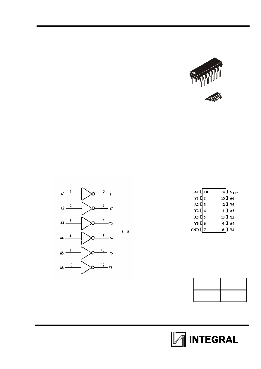
The 74LVU04 is a general purpose hex inverter. Each of the
six
inverters is a single stage with unbuffered outputs.
û Wide Operating Voltage: 1.0ü5.5 V
û Optimized for Low Voltage applications: 1.0ü3.6 V
û Accepts TTL input levels between V
CC
=2.7 V and V
CC
=3.6 V
û Low Input Current
N SUFFIX
PLASTIC
D SUFFIX
SOIC
1
14
1
14
ORDERING INFORMATION
IN74LVU04N
Plastic
IN74LVU04D
SOIC
IZ74LVU04
Chip
T
A
= -40
ú ü 125ú C for all
packages
LOGIC DIAGRAM
PIN 14 =V
CC
PIN 7 = GND
PIN ASSIGNMENT
FUNCTION TABLE
Input Output
A Y
L H
H L
IN74LVU04
2
MAXIMUM RATINGS
*
Symbol Parameter Value
Unit
V
CC
DC supply voltage (Referenced to GND)
-0.5
ü +7.0
V
I
IK
*
1
DC input diode current
20
mA
I
OK
*
2
DC output diode current
50
mA
I
O
*
3
DC output source or sink current
-bus driver outputs
25
mA
I
CC
DC
V
CC
current for types with
- bus driver outputs
50
mA
I
GND
DC GND current for types with
- bus driver outputs
50
mA
P
D
Power dissipation per package, plastic
DIP+
SOIC
package+
750
500
mW
Tstg Storage
temperature
-65
ü +150
úC
T
L
Lead temperature, 1.5 mm from Case for
10 seconds (Plastic DIP ), 0.3 mm (SOIC
Package)
260
úC
*
Maximum Ratings are those values beyond which damage to the device may occur.
Functional operation should be restricted to the Recommended Operating Conditions.
+Derating - Plastic DIP: - 12 mW/
úC from 70ú to 125úC
SOIC Package: : - 8 mW/
úC from 70ú to 125úC
*
1
: V
I
< -0.5V or V
I
> V
CC
+0.5V
*
2
: Vo
< -0.5V or Vo > V
CC
+0.5V
*
3
: -0.5V
< Vo < V
CC
+0.5V
RECOMMENDED OPERATING CONDITIONS
Symbol Parameter Min
Max
Unit
V
CC
DC Supply Voltage (Referenced to
GND)
1.0 5.5 V
V
IN
, V
OUT
DC Input Voltage, Output Voltage
(Referenced to GND)
0 V
CC
V
T
A
Operating Temperature, All Package
Types
-40 +125
úC
t
r
, t
f
Input Rise and Fall
Time
1.0 V
òV
CC
<2.0 V
2.0 V
òV
CC
<2.7 V
2.7 V
òV
CC
<3.6 V
3.6 V
òV
CC
ò5.5 V
0
0
0
0
500
200
100
50
ns
This device contains protection circuitry to guard against damage due to high static
voltages or electric fields. However, precautions must be taken to avoid applications of any voltage
higher than maximum rated voltages to this high-impedance circuit. For proper operation, V
IN
and
V
OUT
should be constrained to the range GND
ò(V
IN
or V
OUT
)
òV
CC
.
Unused inputs must always be tied to an appropriate logic voltage level (e.g., either GND or
V
CC
). Unused outputs must be left open.
IN74LVU04
3
DC ELECTRICAL CHARACTERISTICS (Voltages Referenced to GND)
Guaranteed Limit
25
úC -40úC ü 85úC -40úC ü
125
úC
Symbol Parameter
Test
Conditions
V
CC
,
V
min max min max min max
Unit
V
IH
High-Level
Input Voltage
1.2
2.0
2.7
3.0
3.6
4.5
5.5
1.0
1.6
2.4
2.4
2.4
3.6
4.4
1.0
1.6
2.4
2.4
2.4
3.6
4.4
1.0
1.6
2.4
2.4
2.4
3.6
4.4
V
V
IL
Low -Level
Input Voltage
1.2
2.0
2.7
3.0
3.6
4.5
5.5
-
-
-
-
-
-
-
0.2
0.4
0.5
0.5
0.5
0.9
1.1
-
-
-
-
-
-
-
0.2
0.4
0.5
0.5
0.5
0.9
1.1
-
-
-
-
-
-
-
0.2
0.4
0.5
0.5
0.5
0.9
1.1
V
V
I
= V
IH
or
V
IL
I
0
=-100 A
1.2
2.0
2.7
3.0
3.6
4.5
5.5
1.05
1.85
2.55
2.85
3.45
4.35
5.35
-
-
-
-
-
-
-
1.0
1.8
2.5
2.8
3.4
4.3
5.3
-
-
-
-
-
-
-
1.0
1.8
2.5
2.8
3.4
4.3
5.3
-
-
-
-
-
-
-
V
I
= V
IH
or
V
IL
I
0
=-6.0 mA
3.0
2.48 - 2.40 - 2.20 -
V
OH
High-Level
Output Voltage
V
I
= V
IH
or
V
IL
I
0
=-12 mA
4.5
3.70 - 3.60 - 3.50 -
V
V
I
= V
IH
or
V
IL
I
0
=100 A
1.2
2.0
2.7
3.0
3.6
4.5
5.5
-
-
-
-
-
-
-
0.15
0.15
0.15
0.15
0.15
0.15
0.15
-
-
-
-
-
-
-
0.2
0.2
0.2
0.2
0.2
0.2
0.2
-
-
-
-
-
-
-
0.2
0.2
0.2
0.2
0.2
0.2
0.2
V
I
= V
IH
or
V
IL
I
0
=6.0 mA
3.0 - 0.33 - 0.40 - 0.50
V
OL
Low-Level
Output Voltage
V
I
= V
IH
or
V
IL
I
0
=12 mA
4.5 - 0.40 - 0.55 - 0.65
V
I
IL
Low-Level
Input Leakage
Current
V
I
=0
V 5.5 - -0.1 - -1.0 - -1.0 A
DC ELECTRICAL CHARACTERISTICS (continuation)
IN74LVU04
4
Guaranteed Limit
25
úC -40úC ü 85úC -40úC ü
125
úC
Symbol Parameter
Test
Conditions
V
CC
,
V
min max min max min max
Unit
I
IH
High-Level
Input Leakage
Current
V
I
= V
——
5.5 - 0.1 - 1.0 - 1.0
I
CC
Quiescent
Supply Current
(per Package)
V
I
=0 ¬ or
V
——
I
O
= 0 A
5.5 - 4.0 - 20 - 40 A
I
CC1
Additional
Quiescent
Supply Current
on input
V
I
= V
——
-
0.6V
2.7
3.6
-
-
0.2
0.2
-
-
0.5
0.5
-
-
-
0.85
0.85
mA
AC ELECTRICAL CHARACTERISTICS (C
L
=50 pF, t
LH
=t
HL
= 2.5 ns, R
L
=1 k)
Guaranteed Limit
25
úC -40úC ü
85
úC
-40
úC ü
125
úC
Symbol Parameter
Test
Conditio
ns
V
CC
V
min max min max min max
Unit
t
PHL
(t
PLH)
Propagation
Delay, Input A
to Output Y
(Figure 1 )
V
I
=0 V or
V
1
t
LH
= t
HL
=2.5 ns
—
L
= 50
pF
R
L
= 1
k
1.2
2.0
2.7
3.0
4.5
-
-
-
-
-
70
22
16
13
11
-
-
-
-
-
80
26
19
15
13
-
-
-
-
-
100
31
23
18
16
ns
C
I
Input
Capacitance
5.5
- 7.0 - - - - pF
“
¿
=25
ú—, V
I
=0V or V
CC
pF
C
PD
Power Dissipation Capacitance (Per
Inverter)
36
Used to determine the no-load dynamic power consumption:
P
D
= C
PD
V
CC
2
f
I
+ (C
L
V
CC
2
fo), f
I
- input frequency, fo - output frequency (MHz)
(C
L
V
CC
2
fo) - sum of the outputs
IN74LVU04
5
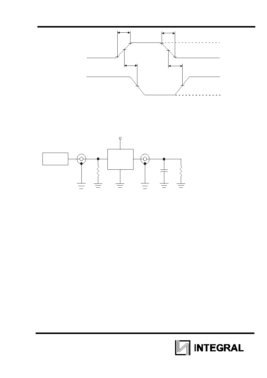
Figure 1. Switching Waveforms
Figure 2. Test circuit
0.1
0.1
0.9
0.9
V
X
V
X
t
PHL
t
HL
t
PLH
t
LH
V
Y
V
Y
Input ¿
Output Y
GND
V
OL
V
1
V
OH
V
X
=0.5 V
CC
PULSE
GENERATOR
DEVICE
UNDER
TEST
V
CC
V
I
V
O
C
L
R
L
R
T
Termination resistance R
T
-
should be equal to Z
OUT
of pulse
generators