TECHNICAL DATA
IN74VHCT373
Octal d-type latch (3-state)
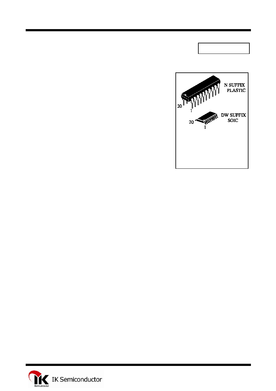
ORDERING INFORMATION
IN74VHCT373N Plastic
IN74VHCT373DW SOIC
T
A
= -40
ú to 85ú C for all packages
IN74VHCT373 is designed for using in up-to-date high
performance computers, high-level electronic equipment
for mass application.
IN74VHCT373 is identical in pinout to the ICs
IN74HC373A, IN74HCT373A, IN74AC373A,
IN74ACT373A.
Input voltage levels are compatible with standard TTL-
levels. Output voltage levels are compatible with input
levels of C-MOS, N-MOS and TTL ICs.
Features:
û
Supply voltage range 4.5 to 5.5 V.
û
Output current 8 mA.
û
Low consumption current: 0.2 mkA (typical value) at “ý = 25
ú—.
û
Latchup current not less than 300 mA at “ý = 85
ú—.
û
Tolerable value of static potential not less than 2000 V as per human body model
(HBM) and not less than 200 V as per machine model (ÃÃ).
û
Ambient operation temperature minus 40 to plus 85
ú—.
û
Balanced signal propagation delay.
û
Ensures voltage exceeding mode on input
.
1
IN74VHCT373
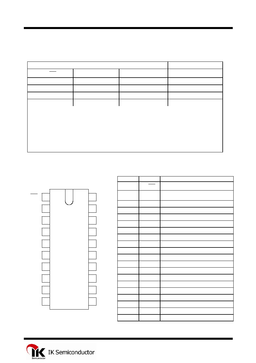
IN74VHCT373 truth table
Input Output
OE
LE D
Q
L H H
H
L H L
L
L L X Qo
H
X
X Z
Note -
H - high voltage level;
L - low voltage level;
X - any voltage level (low or high);
Qo - storage of the previous state;
Z - output in the third state
Pins description in IN74VHCT373
Pin No.
Symbol
Description
01
OE
Input OUTPUT ENABLE
02
Q0 Data
output
03
D0 Data
input
04
D1 Data
input
05
Q1 Data
output
06
Q2 Data
output
07
D2 Data
input
08
D3 Data
input
09
Q3 Data
output
10
GND
Common output
11
LE
Recording enable input
12
Q4 Data
output
13
D4 Data
input
14
D5 Data
input
15
Q5 Data
output
16
Q6 Data
output
17
D6 Data
input
18
D7 Data
input
19
Q7 Data
output
Pinout
01
Q0
02
D0
03
04
05
06
07
08
09
GND
10
20
19
18
17
16
15
14
13
12
11
V
CC
D1
Q1
Q2
D2
D3
Q3
D7
D6
Q6
Q5
D5
D4
Q4
LE
OE
Q7
20
Vcc
Supply output from voltage source
2
IN74VHCT373
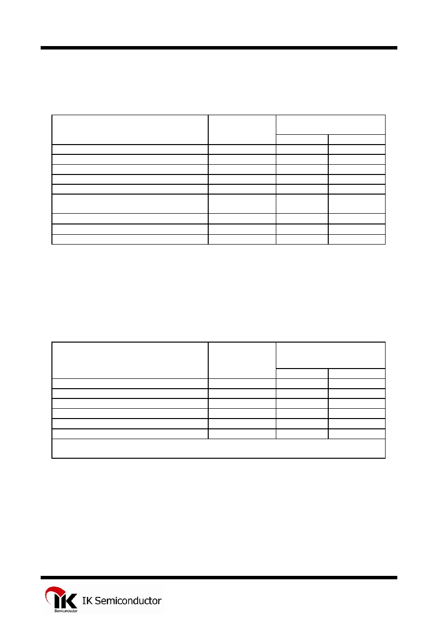
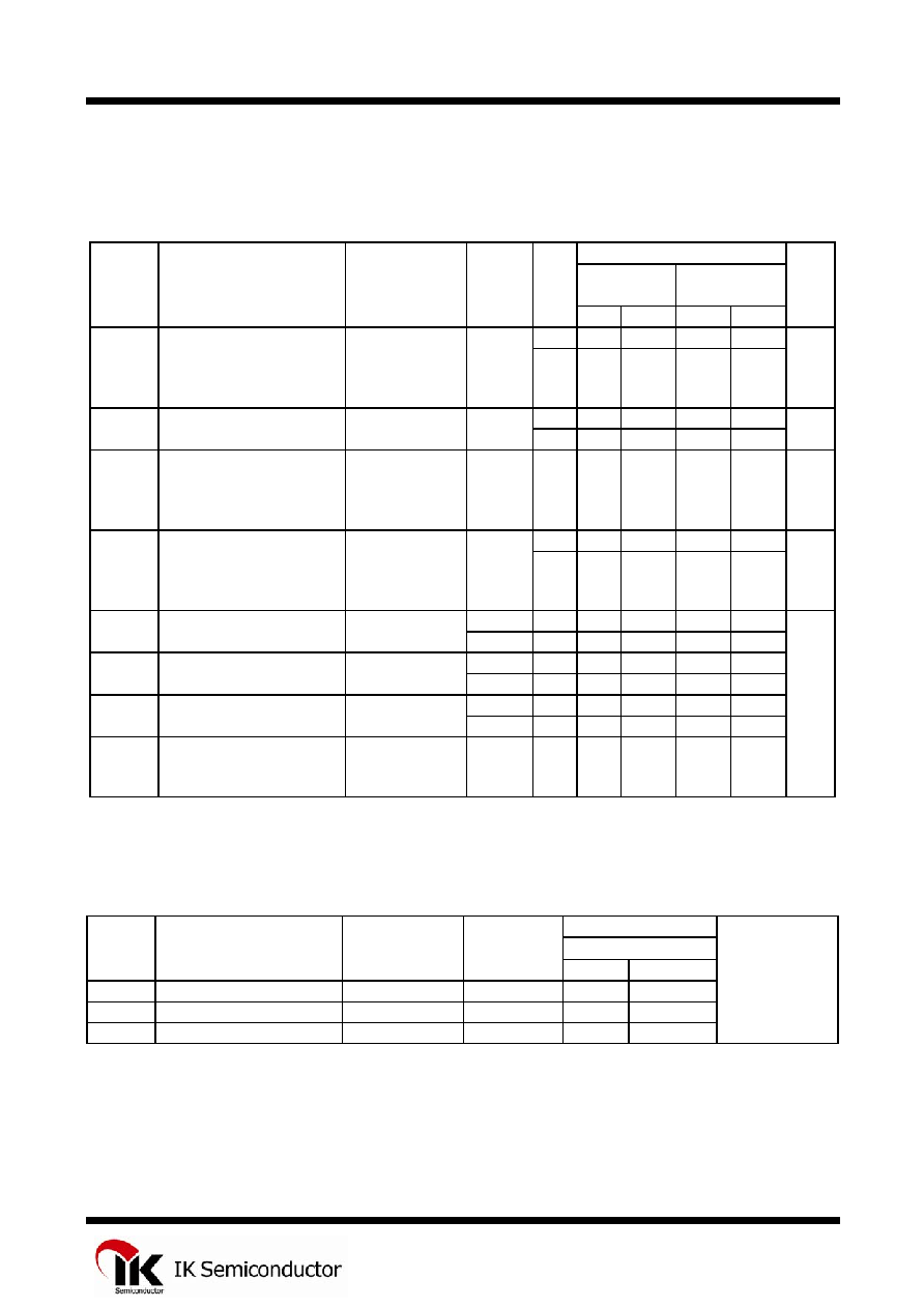
Absolute maximum conditions*
Parameter, unit
Symbol
Value
min
max
Supply voltage, V
V
CC
-0.5 7.0
Input voltage, V
Vin
-0.5
7.0
Output voltage, V
Vout
-0.5
V
CC
+ 0.5B
Output voltage, V
Vout1
-0.5
7.0
Input diode current, mA
Iik
-
-20
Current of common output and supply
output, mA
Icc
75
Output current, mA
Iout
25
Output diode current, mA
Iok
20
Dissipated power, mW
Pd
180
*Under absolute maximum conditions operation of microcircuit is not guaranteed. Operation is
guaranteed under maximum conditions
Maximum conditions
Symbol Value
Parameter, unit
min
max
Supply voltage, V
V
CC
4.5 5.5
Input voltage,V
Vin
0
V
CC
Output voltage, V
Vout
0
V
CC
Output voltage, V
Vout1
0
5.5*
Output current, mA
Iout
-
8.0
Input rise and fall time, ns/V
t
LH
, t
HL
0 20
* - For ICs without third state on outputs - Vcc = 0V, for ICs with third state on outputs - outputs
should be in third state
3
IN74VHCT373
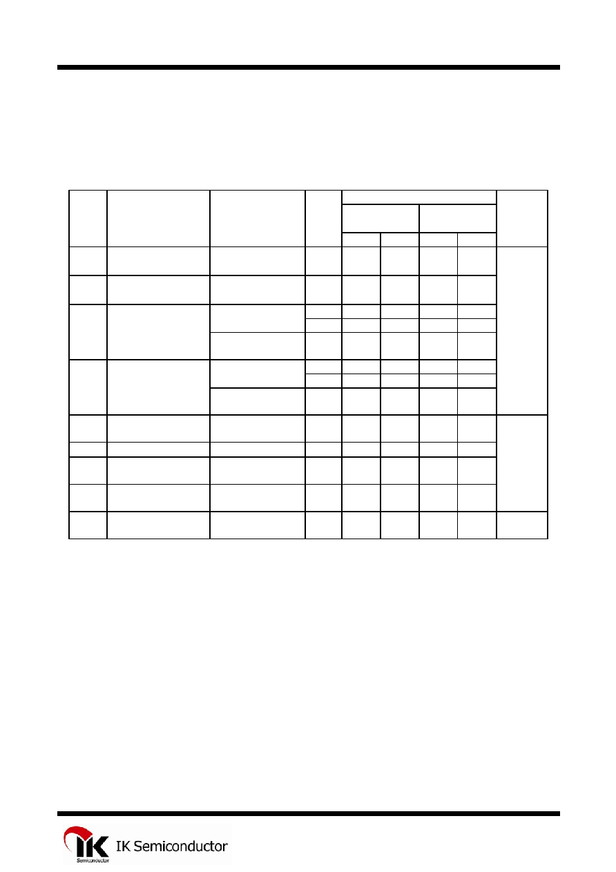
DC electrical characteristics
Value
25
úC
-40
to 85
úC
Symbo
l
Parameter Test
conditions
V
CC
,
V
min max
min max
Unit
V
IH
High input voltage
V
O
ò 0.1 V or
V
O
ô V
CC
-0.1
4.5 -
5.5
2.0
- 2.0
- V
V
IL
Low input voltage
V
O
ò 0.1 V or
V
O
ô V
CC
-0.1
4.5 -
5.5
- 0.8
- 0.8
4.5 4.42
- 4.4 -
V
I
= V
IH
or V
IL
I
O
= -50 mkA
5.5 5.42
- 5.4 -
V
OH
High output voltage
V
I
= V
IH
or V
IL
;
I
O
= -8 mA
4.5 3.94
- 3.80 -
4.5 - 0.09
- 0.1
V
I
= V
IH
or V
IL
I
O
= 50 mkA
5.5 - 0.09
- 0.1
V
OL
Low output voltage
V
I
= V
IH
or V
IL
I
O
= 8 mA
4.5 - 0.36
- 0.44
I
OZ
Output current in
"off" state
V
I
= 2.0V
V
O
= V
CC
or 0V
5.5 -
0.25
-
2.5
I
I
Input current
V
I
= 0 V or V
CC
5.5
0.1
1.0
I
IH1
High level input
current
V
I
= 5.5V
0
-
0.1
-
1.0
uA
I
CC
Consumption current V
I
=V
CC
or 0V
5.5 - 4.0 - 40.0
I
CCT
TTL-input
consumption current
V
I
= 3.4 V
5.5 - 1.35
- 1.5 mA
4
IN74VHCT373
AC electrical characteristics (t
LH
= t
HL
= 3.0 ns, R
L
= 1 kOhm)
Value
25
úC
-40
to 85
úC
Symbol Parameter
Test conditions
V
CC
, V
C
L
,
pF
min
max min max
Unit
15
- 12.3 - 13.5
t
PHL
,
t
PLH
Propagation delay time
when switching on,
off from input LE to
output Q
Fig 1
5.0 0.5
50
- 13.3 - 14.5
ns
15
- 8.5 - 9.5
t
PHL
,
t
PLH
From input D to output Q Fig 1
5.0 0.5
50
- 9.5 - 10.5
ns
t
PHZ
, t
PLZ
Propagation delay time
under transition from
high, low level into off
state
Fig 2
5.0 0.5 50
-
11.2
-
12.0
ns
15
- 10.9 - 12.5
t
PZH
, t
PZL
Propagation delay time
under transition from
off state into high, low
level
Fig 2
5.0 0.5
50
- 11.9 - 13.5
ns
5.0 0.5 15
1.5
-
1.5
-
t
SU
Time of setting signal D
relativey to LE
Fig 3
50
1.5
- 1.5 -
5.0 0.5 15
3.5
-
3.5
-
t
H
Retention time, D signal
to LE
Fig 3
50
3.5
- 3.5 -
5.0 0.5 15
6.5
-
8.5
-
t
W
Pulse duration of LE
signal
Fig 3
50
6.5
- 8.5 -
t
OSLH
,
t
OSHL
Propagation delays
difference between
outputs
-
5.5 0.5 50
-
1.0
-
1.0
ns
Capacitance characteristics
Value
25
úC
Symbol Parameter
Test conditions
V
CC
, V
min max
Unit
C
I
Input capacity
-
5.0
10
pF
C
O
Output capacity
-
5.0
12
pF
C
–D
Dynamic capacity
V
I
= 0 V orV
CC
5.0 50 pF
5