
IN75232
Korzhenevskogo 12, Minsk, 220064, Republic of
Belarus
Fax: +375 (17) 278 28 22,
Phone: +375 (17) 278 07 11, 277 24 70, 277 24 61,
277 69 16
E-mail: belms@belms.belpak.minsk.by
URL: www.bms.by
EIA-232-D INTERFACE 1 CHIP IC
DESCRIPTION
The IN75232 is monolitic device containing 3 independent drivers and 5 receivers. It is
designed to interfase between data terminal equipment and data communication equipment
by EIA-232-D.
FEATURES
û
Meets standard EIA-232-D (Revision of RS-232-C)
û
Drivers
-- Current Limited Output .... 10 mA Typical
-- Power-off Output Impedance .... 300
Min
-- Slew Rate Control by Load Capacitor
-- Flexible Supply Voltage Range
-- Input Compatible with Most TTL and DTL Circuits
û
Receiver
-- Input Resistance ......... 3 k
to 7 k
-- Input Signal Range ......
30 V
-- Built-in Input Hysteresis (Double Threshold)
û
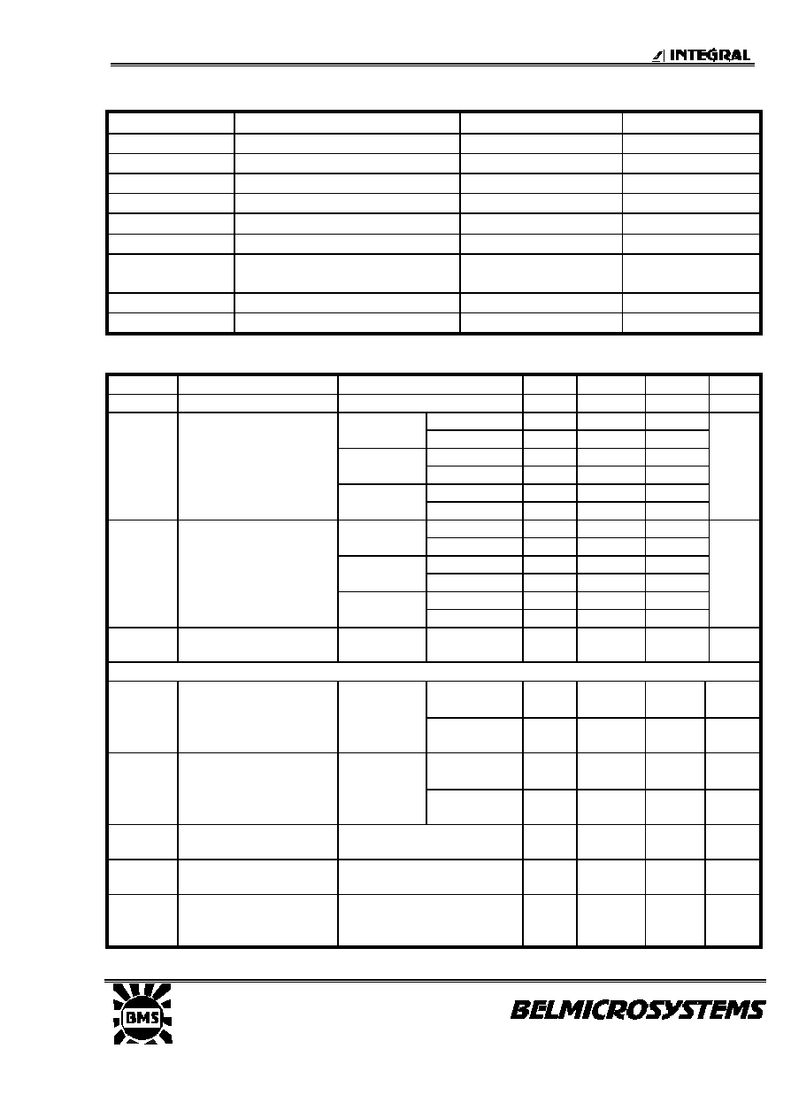
20 DIP/SOP
2
6
4
5
19
3
18
17
16
15
7
14
8
13
9
12
10
11
1
20
V
C C
+
RA1
RA2
RA3
DY1
DY2
RA4
DY3
RA5
V
C C
-
V
C C
RY1
RY2
RY3
DA1
DA2
RY4
DA3
RY5
GND
Block Diagram
PIN DESCRIPTION
Name
Pin No
Function
Name
Pin No
Function
Vcc+
1
Driver Section Supply
Vcc-
10
Driver Section Supply --
DA1
16
DY1
5
DA2
15
Driver Input
DY2
6
Driver Output
DA3
13
DY3
8
Vcc
20
Receiver Section Supply
GND
11
Ground
RA1
2
RY1
19
RA2
3
RY2
18
RA3
4
Receiver Input
RY3
17
Receiver Output
RA4
7
RY4
14
RA5
9
RY5
12
IN75232
Korzhenevskogo 12, Minsk, 220064, Republic of
Belarus
Fax: +375 (17) 278 28 22,
Phone: +375 (17) 278 07 11, 277 24 70, 277 24 61,
277 69 16
E-mail: belms@belms.belpak.minsk.by
URL: www.bms.by
ABSOLUTE MAXIMUM RATINGS
Symbol
Parametr
Rating
Unit
Vcc+
Supply Voltage
15
V
Vcc-
Supply Voltage
-15
V
Vcc
Supply Voltage
10
V
VI (Driver)
Input Voltage
-15...+7
V
VI (Receiver)
Input Voltage
30
V
VO (Driver)
Output Voltage
-15...+15
V
PT
Continuous Power Dissipation
(Below 25
o
C)
1.0
W
T
STG
Storage Tempetatura
-65...+175
o
C
T
OP
Operating Tempetatura
0...+75
o
C
ELECTRICAL CHARACTERISTICS
Supply Current
Symbol
Parameter
Test Condition
Min
Typ
Max
Unit
1
2
3
4
5
6
7
Icc+
Supply Current
Vcc+=9V
Vin=1.9V
11.3
15
from Vcc+
No Load
Vin=0.8V
3.4
4.5
Vcc+=12V
Vin=1.9V
14.3
19
mA
No Load
Vin=0.8V
4.1
5.5
Vcc+=15V
Vin=1.9V
25
No Load
Vin=0.8V
9
Icc-
Supply Current
Vcc+=-9V
Vin=1.9V
-12
-15
from Vcc-
No Load
Vin=0.8V
-3.2
Vcc+=-12V
Vin=1.9V
-16
-19
mA
No Load
Vin=0.8V
-3.2
Vcc+=-15V
Vin=1.9V
-25
No Load
Vin=0.8V
-3.2
Icc
Supply Current
from Vcc
Vcc=5V
Vin=5V
20
30
mA
Driver Section
V
OH
High Level
Output Voltage
V
IL
=0.8V
R
L
=3 k
Vcc+=9V
Vcc-=-9V
6
7
V
Vcc+=13.2V
Vcc-=-13.2V
9
10.5
V
OL
Low Level
Output Voltage
V
IL
=1.9V
R
L
=3 k
Vcc+=9 V
Vcc-=-9V
-6
V
Vcc+=13.2V
Vcc-=-13.2V
-9
I
IH
High Level
Input Current
V
I
=5V
10
A
I
IL
Low Level
Input Current
V
I
=0
-1
-1.6
mA
I
OS
(H)
Short Circuit
Output Current
at High Level
V
I
=0.8V
V
O
=0
-6
-10
-12
mA

IN75232
Korzhenevskogo 12, Minsk, 220064, Republic of
Belarus
Fax: +375 (17) 278 28 22,
Phone: +375 (17) 278 07 11, 277 24 70, 277 24 61,
277 69 16
E-mail: belms@belms.belpak.minsk.by
URL: www.bms.by
ELECTRICAL CHARACTERISTICS
Supply Current
Symbol
Parameter
Test Condition
Min
Typ
Max
Unit
1
2
3
4
5
6
7
I
OS
(L)
Short Circuit
Output Current
at Low Level
V
I
=1.9V
V
O
=0
6
10
12
mA
R
O
Output Resistance,
Power Off
Vcc+=0, Vcc-=0
V
O
= -2V to 2V
300
Driver Switching Characteristics ( Vcc+=9V, Vcc-=-9V, T
A
=25
o
C)
t
PLH
Propogation Delay
Time, Low-To-High
Level Output
R
L
=3 k
C
L
=15 pF
400
500
ns
t
PHL
Propogation Time,
High -To- Low Level
Output
100
175
ns
t
THL
Transition Delay Time,
Low-To-High Level
Output
55
100
bns
t
TLH
Transition Delay Time,
High-To-Low Level
Output
45
75
ns
Receiver Section
V
OH
High Level
Output Voltage
V
I
=0.75V, I
OL
=-0,5 mA
Input Open, I
OL
=-0,5 mA
2.6
2.6
4
4
5
5
V
V
OL
Low Level
Output Voltage
V
I
=3V, I
OL
=10 mA
0.2
0,45
V
I
IH
High-Level Input
Current
V
I
=25V
V
I
=3V
3.6
0.43
8.3
V
I
IL
Low-Level Input
Current
V
I
=-25V
V
I
=-3V
-3.6
-0.43
-8.3
mA
VT+
Positive-Going
Thrteshold Voltage
1.75
1.9
2.25
mA
VT-
Negative-Going
Thrteshold Voltage
0.75 0.97
1.25
V
Receiver Switching Characteristics Vcc=5V
t
PLH
Propogation Delay
Time, Low-To-High
Level Output
C
L
=15 pF
R
L
=3.9 k
100
150
ns
t
PHL
Propogation Time,
High -To- Low Level
Output
C
L
=15 iO
R
L
=390 k
25
50
ns
t
THL
Transition Delay Time,
Low-To-High Level
Output
C
L
=15 pF
R
L
=3.9 k
120
175
ns
t
TLH
Transition Delay Time,
High-To-Low Level
Output
C
L
=15 pF
R
L
=390 k
10
20
ns