 | –≠–ª–µ–∫—Ç—Ä–æ–Ω–Ω—ã–π –∫–æ–º–ø–æ–Ω–µ–Ω—Ç: IND16305 | –°–∫–∞—á–∞—Ç—å:  PDF PDF  ZIP ZIP |

IND16305
Korzhenevsky 12, Minsk, 220064, Republic of Belarus
Fax: +375 (17) 278 28 22
Tel: +375 (17) 278 49 09, 212 27 02
Tel/fax: +375 (17) 212 68 53
E-mail: office@bms.by
URL: www.bms.by
1
40-BIT AC-PDP DRIVER
DESCRIPTION
The IND16305 is an AC plasma display panel (PDP) row driver which uses a high withstand voltage CMOS process. It
is composed of a 40-bit bidirectional shift register, latch circuit, and a high withstand voltage CMOS driver block. The
logic block operates on a 5 V power supply (CMOS level input), enabling direct connection to a microcomputer. The
driver block is implemented by means of 200 V, 400 mA high withstand voltage CMOS.
FEATURES
û
High withstand voltage CMOS structure
û
High withstand voltage, high current output (200 V, 400 mA)
û
On-chip 40-bit bidirectional shift register
û
Low power dissipation (1 mA max. Ta = -40 to +85 C)
û
Wide operating temperature range (-40 to +85 C)
BLOCK DIAGRAM
ABSOLUTE MAXIMUM RATINGS
(Ta = 25
o
C, V
SS1
= V
SS2
= 0 V)
PARAMETER SYMBOL
RATING UNIT
Logic block supply voltage
V
DD1
-0.5 to +7.0
V
Driver block supply voltage
V
DD2
-0.5 to +200
V
Logic block input voltage
V
I
-0.5 to VDD1 + 0.5
V
Driver block output current
I
O
400*
mA
Permissible package loss
P
D
1000
mW
Operating temperature
Topt.
-40 to +85
o
C
Storage temperature
Tsrg.
-65 to +150
o
C
* Duty
ò 1/40. Derate at -10 mW/
o
C at T
A
= 25
o
C or higher
RECOMMENDED OPERATING CONDITIONS
(Ta = -40 to + 85
o
C, V
SS1
= V
SS2
= 0 V)
PARAMETER SYMBOL
MIN.
TYP.
MAX.
UNIT
Logic block supply voltage
V
DD1
4.5
5.0
5.5
V
Driver block supply voltage
V
DD2
30
180
V
Input voltage high
V
IH
0.8 û V
DD1
V
DD1
V
Input voltage low
V
IL
0
0.2 û V
DD1
V
Driver output current
I
O
300
mA
S
1
S
40
I/O
O
40
O
1
L
1
PC
BLK
STB
A
CLK
R/L
B
*
I/O
40-Bit
shift
Register
40-Bit
Latch
*
BLK
CLR
CLR
* High Withstand Voltage CMOS
Driver Block 200V, 400mA max
IND16305
Korzhenevsky 12, Minsk, 220064, Republic of Belarus
Fax: +375 (17) 278 28 22
Tel: +375 (17) 278 49 09, 212 27 02
Tel/fax: +375 (17) 212 68 53
E-mail: office@bms.by
URL: www.bms.by
2
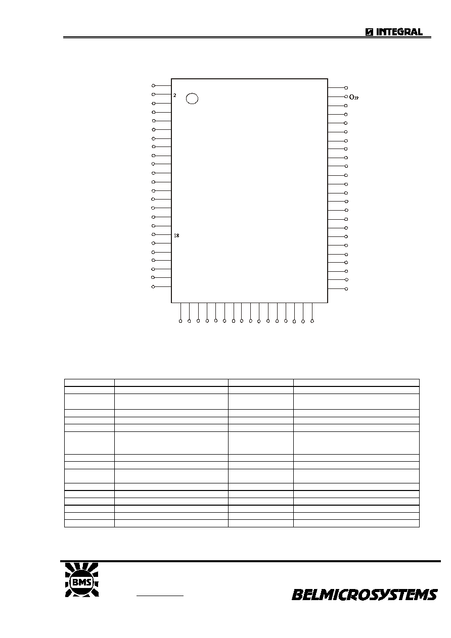
PIN CONFIGURATION (Top View)
û
Ensure that the V
DD1
, V
DD2
, V
SS1
and V
SS2
pins are all used, and that V
SS1
and V
SS2
are used at the same potential
(connect at same point near IC).
û
Pin 33 is connected to the lead frame, and must therefore be left open.
DESCRIPTION OF PINS
Pin Symbol
Pin Name
Pin No.
Description
BLK
Output blank input
37
See truth table
A
RIGHT data input/output
30
Serial data input/output* When R/L = H
A: Input B:Output
B
LEFT data input/output
35
When R/L = L A: Output B: Input
CLK
Clock input
31
Shift executed on rise
STB
Latch enable input
36
H: Latch, L: Data-through
R/L
Shift direction control input
25
H: Right shift modeA
O
1
ûûûO
40
B
L : Left shift mode B
O
40
ûûûO
1
A
CLR
Clear input
32
L: Shift register ALL L
PC
Polarity reversal input
27
See truth table
O
1
to O
40
High withstand voltage outputs
1 to 20
45 to 64
200 V, 400 mA max.
V
DD1
Logic block power supply
26, 39
5 V 10 %
V
DD2
Driver block power supply
21, 44
30 V to 180 V
V
SS1
Logic block ground
24, 41
Connect to system GND
V
SS2
Driver block ground
22, 23, 42, 43
Connect to system GND at same point.
NC
Unused pins
28, 29, 33,
Non-connection
34, 38, 40
Ensure that pin 33 is left open.
*
Data resulting from inversion of the data input is input to the shift register, and data resulting from inversion of the shift
register data is output to the output.
64
63
62
61
60
59
58
57
56
55
54
53
52
51
25 26 27 28 29 30 31 32 33 34 35 36 37 38 39 40
1
3
4
5
6
7
8
9
10
11
13
14
15
16
17
19
20
21
22
23
24
12
V
DD2
V
SS2
O
6
O
7
O
8
O
9
O
10
O
11
O
12
O
13
O
14
O
15
O
16
O
17
O
18
O
19
O
20
CL
R
C
LK
A
NC
V
DD
1
PC
BLK
NC
V
SS2
V
SS1
O
1
O
2
O
3
O
4
O
5
R/L
B
NC
NC
STB
NC
V
DD
1
NC
50
49
48
47
46
45
44
43
42
41
V
DD2
V
SS2
O
35
O
34
O
33
O
32
O
31
O
30
O
29
O
28
O
27
O
26
O
25
O
24
O
23
O
22
O
21
V
SS2
V
SS1
O
40
O
38
O
37
O
36
IND16305
Korzhenevsky 12, Minsk, 220064, Republic of Belarus
Fax: +375 (17) 278 28 22
Tel: +375 (17) 278 49 09, 212 27 02
Tel/fax: +375 (17) 212 68 53
E-mail: office@bms.by
URL: www.bms.by
3
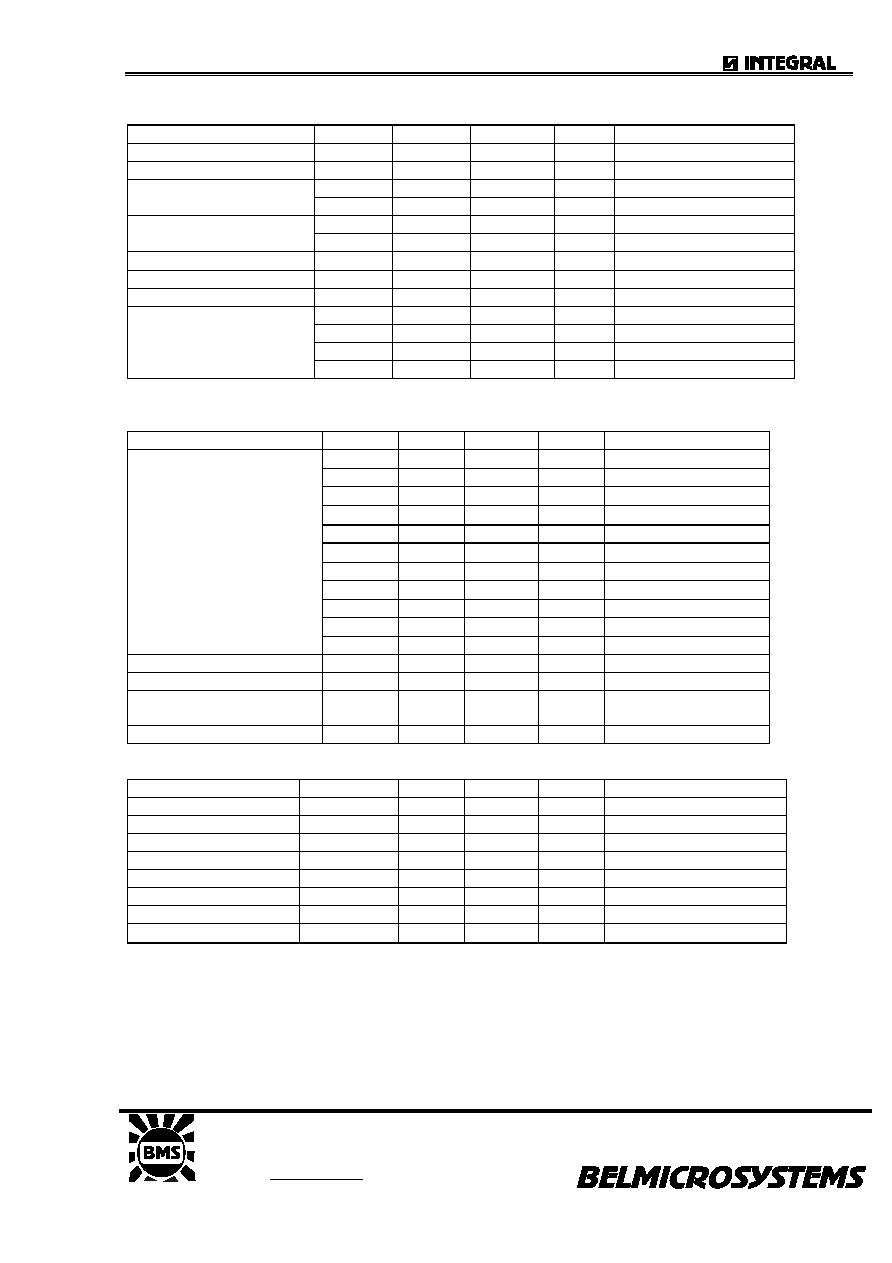
ELECTRICAL SPECIFICATIONS
(Ta = 25
o
C, V
DD1
= 4.5 to 5.5 V, V
DD2
= 180 V, V
SS1
= V
SS2
= 0 V)
PARAMETER SYMBOL
MIN.
MAX.
UNIT
TEST
CONDITIONS
Output voltage high
V
OH1
0.9 û V
DD1
V
Logic
I
OH
= -1 mA
Output voltage low
V
OL1
0.1 û V
DD1
V
Logic
I
OL
= 1 mA
V
OH21
160
V O
1
to O
40
, I
OH
= -150 mA
Output voltage high
V
OH22
140
V O
1
to O
40
, I
OH
= -300 mA
V
OL21
20
V O
1
to O
40
, I
OL
= 150 mA
Output voltage low
V
OL22
40
V O
1
to O
40
, I
OL
= 300 mA
Input current
I
I
1
uA V
I
= V
DD1
or V
SS1
Input voltage high
V
IH
0.8 û V
DD1
V
Input voltage low
V
IL
0.2 û V
DD1
V
I
DD1
100
uA
Logic Ta = -40 to +85
o
C
I
DD1
10
uA
Logic Ta = 25
o
C
I
DD2
1
mA
Driver Ta = -40 to +85
o
C
Static comsumption current
I
DD2
100
uA
Driver Ta = 25
o
C
SWITCHING CHARACTERISTICS (T
a
= 25
o
C, V
DD1
= 5 V, V
DD2
= 180 V, Logic C
L
= 15 pF, Driver C
L
= 50
pF)
PARAMETER SYMBOL
MIN.
MAX.
UNIT
TEST
CONDITIONS
t
PHL1
120 ns CLK
A/B
t
PLH1
120 ns
t
PLH2
120 ns CLR
A/B
t
PHL3
200 ns CLK
O1 to O40
t
PLH3
200 ns
t
PHL4
200 ns STB
O1 to O40
t
PLH4
200 ns
t
PHL5
220 ns BLK
O1 to O40
t
PLH5
220 ns
t
PHL6
220 ns PC
O1 to O40
Transmission delay time
t
PLH6
220 ns
Rise time
t
TLH
100
ns
O1 to O40
Fall time
t
THL
100
ns
O1 to O40
Maximum clock frequency
(DATA)
f
max
.
15
MHz
Duty = 50 %
Input capacitance
C
I
15 pF
REQUIRED TIMING CONDITIONS (T
a
= -40 to +85
o
C, V
DD1
= 4.5 to 5.5 V)
PARAMETER SYMBOL
MIN.
MAX.
UNIT
TEST
CONDITIONS
Clock pulse width
PW
CLK
30
ns
Strobe pulse width
PW
STB
60
ns
Blank pulse width
PW
BLK
200
ns
PC pulse width
PW
PC
300
ns
Clear pulse width
PW
CLR
120
ns
Data setup time
t
SETUP
20
ns
Data hold time
t
HOLD
5
ns
Clock-strobe time
t
CLK-STB
120
ns CLK
STB

IND16305
Korzhenevsky 12, Minsk, 220064, Republic of Belarus
Fax: +375 (17) 278 28 22
Tel: +375 (17) 278 49 09, 212 27 02
Tel/fax: +375 (17) 212 68 53
E-mail: office@bms.by
URL: www.bms.by
4
TRUTH TABLE 1 (Shift Register Block)
R/L CLK A
B
Shift
Register
H
Input
Output
Right shift execution
H
H or L
Hold
L
Output Input
Left shift execution
L
H or L
Hold
TRUTH TABLE 2 (Latch Block)
STB Operation
H
Data immediately prior to STB becoming H is held
L
Shift register data is output
TRUTH TABLE 3 (Driver Block)
DATA BLK PC On
Remarks
H L
L
H
L L
L
L
H L
H
L
L L
H
H
’ H
L
H All outputs H
’ H
H
L All outputs L
H
: High level
L
: Low level
’
: H or L
DATA: Data input to A (B)
Caution To prevent latch up breakdown, the power should be turned on in the order V
DD1
, logic signal, V
DD2
.
It should be turned off in the opposite order.
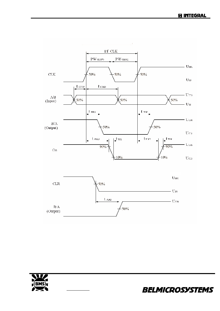
TIMING CHART
( ): When R/L=L
IND16305
Korzhenevsky 12, Minsk, 220064, Republic of Belarus
Fax: +375 (17) 278 28 22
Tel: +375 (17) 278 49 09, 212 27 02
Tel/fax: +375 (17) 212 68 53
E-mail: office@bms.by
URL: www.bms.by
5
SWITCHING CHARACTERISTIC WAVEFORMS