INF85116
1
WP
n. c.
n. c.
n. c.
Uss
Ucc
SCL
INF85116N
SDA
1
2
3
4
8
7
6
5
2048 ı 8 -Bit CMOS EEPROM with I
2
—-bus interface
The INF85116N is an 16-Kbits (2048 x 8-bit) floating
gate Electrically Erasable Programmable Read Only
Memory (EEPROM). Power consumption is low due to
the full CMOS technology used. The programming
voltage is generated on-chip, using a voltage multi-
plier. As data bytes are received and transmitted via
the serial I
2
C-bus, a package using eight pins is suffi-
cient. Only one INF85116N device is required to sup-
port all eight blocks of 256 x 8-bit each.
FEATURES
û Low power CMOS
-maximum active current 1.0 mA
-maximum standby current 10
A (at 5.5 V), typical 4 A
û Non-volatile storage of 16-Kbits organized as eight blocks of 256x8-bits during 20 years
( at 55
o
C )
û Single supply (Ucc=2,7 ü 5,5 V);
û Automatically increased word's address
û On-chip voltage multiplier
û Serial input/output I
2
C-bus
û 1000000 ERASE/WRITE cycles per byte
û Internal timer for writing (no external components)
û Write operations: multi byte write mode to 32 bytes
û Write - protection input
û Power-on-reset
Temperature range: -40
o
C
ü +85
o
C
Simbol Pin
Description
n. c.
n. c
n. c
Uss
SDA
SCL
WP
Ucc
1
2
3
4
5
6
7
8
not connected
not connected
not connected
negative supply voltage
serial data input/output ( I
2
C-
bus)
serial clock input ( I
2
C-bus)
write - protection input
positive supply voltage
Table 1. Quick reference data
Symbol Parameter min
max
Unit
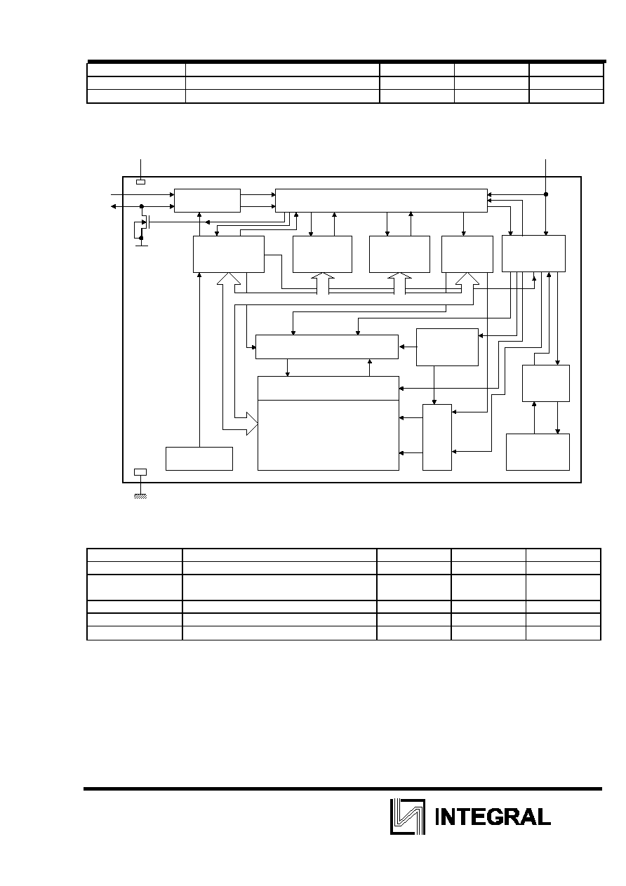
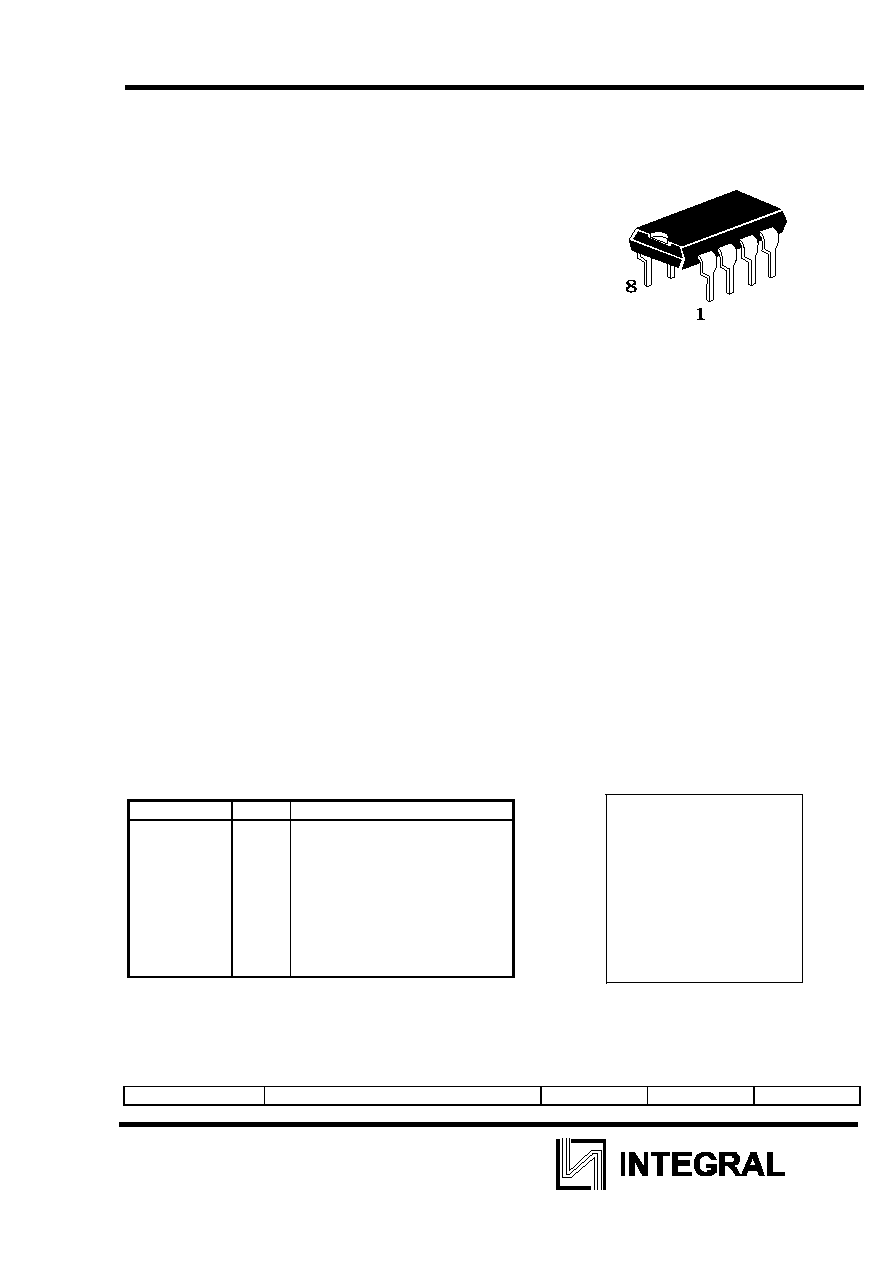
PIN CONFIGURATION
PIN DESCRIPTION

INF85116
3
Table 3. Characteristics
Symbol Parameter
Conditions
min
max
Unit
I
DD(stb)
Standby supply current
U
DD
= 2.7V
U
DD
= 5.5V
- 6
10
¿
¿
I
CCR
Supply current READ
f
S—L
=400ÍHz,
U
DD
= 5.5V
- 1
m¿
I
CCW
Supply current E / W
f
S—L
=400ÍHz,
U
DD
= 5.5V
- 1
m¿
WP input (pin 7)
U
IL
LOW level input voltage
-0.8
+0.1U
DD
V
U
IH
HIGH level input voltage
0.9U
DD
U
DD
+0.8 V
SCL input (pin 6)
U
IL
LOW level input voltage
-0.8
+0.3U
DD
V
U
IH
HIGH level input voltage
0.7U
DD
6.5 V
I
LI
Input leakage current
U
I
=U
DD
or U
SS
-
1
¿
f
SCL
Clock input frequency
0
400
kHz
t
sp
Pulse width of spikes sup-
pressed
by filter
0
100
ns
—
I
Input capacitance
U
I
= U
SS
-
7
pF
SDA input/output (pin 5)
U
IL
LOW level input voltage
-0.8
0.3U
DD
V
U
IH
HIGH level input voltage
0.7U
DD
6.5 V
U
OL1
U
OL2
LOW level output voltage
I
OL
=3m¿,
U
DD
= U
DD (min)
I
OL
=6m¿,
U
DD
= U
DD (min)
- 0.4
0.6
V
I
LO
Output leakage current
U
OH
=U
DD
-
1
¿
t
O(F)
Output fall time from U
IHmin
to U
ILmax
with up to 3m¿ sink
current at U
OL1
with up to 6m¿ sink
current at U
OL2
20+0.1 C
B
*
20+0.1 C
B
250
250
ns
ns
t
SP
Pulse width of spikes sup-
pressed
by filter
0
100
ns
—
I
Input capacitance
U
I
=0V -
10
pF
t
E/W
E/W cycle time
-
10
ms
N
E/W
E/W cycle per byte
“
amb
=(-40-+85)
Ó
—,
“
amb
=22
Ó
—
100000
1000000
-
t
S
Data retention time
“
amb
= 55
Ó
— 20
-
years
- The bus capacitance ranges from 10 to 400pF ( C
B
= total capacitance of one bus line in pF)

INF85116
4
“ýble 4. I
2
C-bus characteristics
Symbol Parameter Condi-
tions
Standard
mode
Fast mode
Unit
min
max
min
max
f
SCL
Clock
frequency
0
100
0
400
kHz
t
BUF
Time the bus must be free before
-
4.7
-
1.3
-
s
t
HD, STA
START condition hold time after which
first clock pulse is generated
- 4.0
-
0.6
-
s
t
LOW
LOW level clock period
-
4.7
-
1.3
-
s
t
HIGH
HIGH level clock period
-
4.0
-
0.6
-
s
t
SU, STA
Set-up time for START condition
repeated
start
4.7 - 0.6 -
s
t
HD, DAT
Data hold time for CBUS compatible
masters
- 5
-
-
-
s
t
HD, DAT
Data hold time for I
2
C - bus devices
note 1
0
-
0
-
ns
t
SU, DAT
Data set-up time
-
250
-
100
-
ns
t
R
SDA and SCL rise time
-
-
1000
20+0.
1 C
b
(2)
300 ns
t
F
SDA and SCL fall time
-
-
300
20+0.
1 C
b
(2)
300 ns
t
SU, STO
Set-up time for STOP condition
-
4.0
-
0.6
-
s
Notes:
1. The hold time required (not greater than 300 ns) to bridge the undefined region of the falling edge of
SCL must be internally provided by a transmitter.
2. C
b
= total capacitance of one bus line in pF.