 | –≠–ª–µ–∫—Ç—Ä–æ–Ω–Ω—ã–π –∫–æ–º–ø–æ–Ω–µ–Ω—Ç: IW4028BD | –°–∫–∞—á–∞—Ç—å:  PDF PDF  ZIP ZIP |
TECHNICAL DATA
59
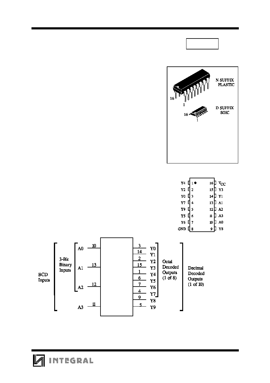
BCD-to-Decimal Decoder
High-Voltage Silicon-Gate CMOS
The IW4028B types are BCD-to-decimal or binary-to-octal
decoders consisting of buffering on all 4 inputs, decoding-logic gates,
and 10 output buffers. A BCD code applied to the four inputs, A0 to
A3 results in a high level at the selected one of 10 decimal decoded
outputs. Similarly, a 3-bit binary code applied to inputs A0 through A2
is decoded in octal code at output 0 to7 if A3="0". High drive
capability is provided at all outputs to enhance dc and dynamic
performance in high fan-out applications.
û
BCD-to-decimal decoding or binary-to-octal decoding
û
Operating Voltage Range: 3.0 to 18 V
û
Maximum input current of 1
A at 18 V over full package-
temperature range; 100 nA at 18 V and 25
ú
C
û
Noise margin (over full package temperature range):
1.0 V min @ 5.0 V supply
2.0 V min @ 10.0 V supply
2.5 V min @ 15.0 V supply
IW4028B
ORDERING INFORMATION
IW4028BN Plastic
IW4028BD SOIC
T
A
= -55
ú
to 125
ú
C for all packages
PIN ASSIGNMENT
LOGIC DIAGRAM
PIN 16=V
CC
PIN 8= GND
IW4028B
60
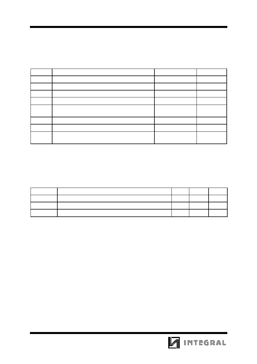
MAXIMUM RATINGS
*
Symbol
Parameter
Value
Unit
V
CC
DC Supply Voltage (Referenced to GND)
-0.5 to +20
V
V
IN
DC Input Voltage (Referenced to GND)
-0.5 to V
CC
+0.5
V
V
OUT
DC Output Voltage (Referenced to GND)
-0.5 to V
CC
+0.5
V
I
IN
DC Input Current, per Pin
10
mA
P
D
Power Dissipation in Still Air, Plastic DIP+
SOIC Package+
750
500
mW
P
D
Power Dissipation per Output Transistor
100
mW
Tstg
Storage Temperature
-65 to +150
ú
C
T
L
Lead Temperature, 1 mm from Case for 10 Seconds
(Plastic DIP or SOIC Package)
260
ú
C
*
Maximum Ratings are those values beyond which damage to the device may occur.
Functional operation should be restricted to the Recommended Operating Conditions.
+Derating - Plastic DIP: - 10 mW/
ú
C from 65
ú
to 125
ú
C
SOIC Package: : - 7 mW/
ú
C from 65
ú
to 125
ú
C
RECOMMENDED OPERATING CONDITIONS
Symbol
Parameter
Min
Max
Unit
V
CC
DC Supply Voltage (Referenced to GND)
3.0
18
V
V
IN
, V
OUT
DC Input Voltage, Output Voltage (Referenced to GND)
0
V
CC
V
T
A
Operating Temperature, All Package Types
-55
+125
ú
C
This device contains protection circuitry to guard against damage due to high static voltages or electric
fields. However, precautions must be taken to avoid applications of any voltage higher than maximum rated
voltages to this high-impedance circuit. For proper operation, V
IN
and V
OUT
should be constrained to the range
GND
ò
(V
IN
or V
OUT
)
ò
V
CC
.
Unused inputs must always be tied to an appropriate logic voltage level (e.g., either GND or V
CC
).
Unused outputs must be left open.
IW4028B
61
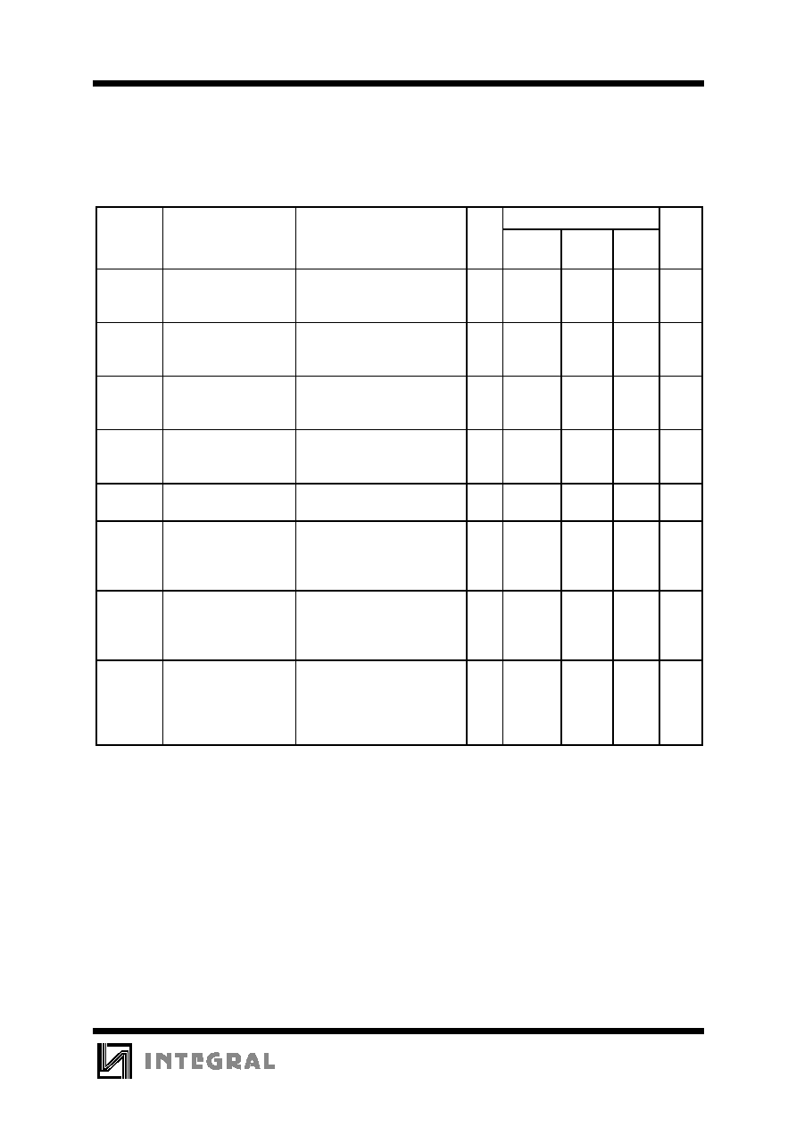
DC ELECTRICAL CHARACTERISTICS
(Voltages Referenced to GND)
V
CC
Guaranteed Limit
Symbol
Parameter
Test Conditions
V
ô
-55
ú
C
25
ú
C
ò
125
ú
C
Unit
V
IH
Minimum High-Level
Input Voltage
V
OUT
= 0.5 V or V
CC
- 0.5V
V
OUT
= 1.0 V or V
CC
- 1.0 V
V
OUT
= 1.5 V or V
CC
- 1.5V
5.0
10
15
3.5
7
11
3.5
7
11
3.5
7
11
V
V
IL
Maximum Low -Level
Input Voltage
V
OUT
= 0.5 V or V
CC
- 0.5V
V
OUT
= 1.0 V or V
CC
- 1.0 V
V
OUT
= 1.5 V or V
CC
- 1.5V
5.0
10
15
1.5
3
4
1.5
3
4
1.5
3
4
V
V
OH
Minimum High-Level
Output Voltage
V
IN
=GND or V
CC
5.0
10
15
4.95
9.95
14.95
4.95
9.95
14.95
4.95
9.95
14.95
V
V
OL
Maximum Low-Level
Output Voltage
V
IN
=GND or V
CC
5.0
10
15
0.05
0.05
0.05
0.05
0.05
0.05
0.05
0.05
0.05
V
I
IN
Maximum Input
Leakage Current
V
IN
= GND or V
CC
18
0.1
0.1
1.0
A
I
CC
Maximum Quiescent
Supply Current
(per Package)
V
IN
= GND or V
CC
5.0
10
15
20
5
10
20
100
5
10
20
100
150
300
600
3000
A
I
OL
Minimum Output Low
(Sink) Current
V
IN
= GND or V
CC
U
OL
=0.4 V
U
OL
=0.5 V
U
OL
=1.5 V
5.0
10
15
0.64
1.6
4.2
0.51
1.3
3.4
0.36
0.9
2.4
mA
I
OH
Minimum Output
High (Source) Current
V
IN
= GND or V
CC
U
OH
=2.5 V
U
OH
=4.6 V
U
OH
=9.5 V
U
OH
=13.5 V
5.0
5.0
10
15
-2
-0.64
-1.6
-4.2
-1.6
-0.51
-1.3
-3.4
-1.15
-0.36
-0.9
-2.4
mA

IW4028B
62
AC ELECTRICAL CHARACTERISTICS
(C
L
=50pF, R
L
=200k
, Input t
r
=t
f
=20 ns)
V
CC
Guaranteed Limit
Symbol
Parameter
V
ô
-55
ú
C
25
ú
C
ò
125
ú
C
Unit
t
PHL
, t
PLH
Maximum Propagation Delay, Input A to Output
Y (Figure 1)
5.0
10
15
350
160
120
350
160
120
700
320
240
ns
t
THL
, t
TLH
Maximum Output Transition Time, Any Output
(Figure 1)
5.0
10
15
200
100
80
200
100
80
400
200
160
ns
C
IN
Maximum Input Capacitance
-
7.5
pF
FUNCTION TABLE
Inputs
Outputs
A3
A2
A1
A0
Y0
Y1
Y2
Y3
Y4
Y5
Y6
Y7
Y8
Y9
L
L
L
L
H
L
L
L
L
L
L
L
L
L
L
L
L
H
L
H
L
L
L
L
L
L
L
L
L
L
H
L
L
L
H
L
L
L
L
L
L
L
L
L
H
H
L
L
L
H
L
L
L
L
L
L
L
H
L
L
L
L
L
L
H
L
L
L
L
L
L
H
L
H
L
L
L
L
L
H
L
L
L
L
L
H
H
L
L
L
L
L
L
L
H
L
L
L
L
H
H
H
L
L
L
L
L
L
L
H
L
L
H
L
L
L
L
L
L
L
L
L
L
L
H
L
H
L
L
H
L
L
L
L
L
L
L
L
L
H
H
L
H
L
L
L
L
L
L
L
L
L
L
L
H
L
H
H
L
L
L
L
L
L
L
L
L
L
H
H
L
L
L
L
L
L
L
L
L
L
L
L
H
H
L
H
L
L
L
L
L
L
L
L
L
L
H
H
H
L
L
L
L
L
L
L
L
L
L
L
H
H
H
H
L
L
L
L
L
L
L
L
L
L
IW4028B
63
Figure 1. Switching Waveforms
EXPANDED LOGIC DIAGRAM