 | –≠–ª–µ–∫—Ç—Ä–æ–Ω–Ω—ã–π –∫–æ–º–ø–æ–Ω–µ–Ω—Ç: 28F016S3 | –°–∫–∞—á–∞—Ç—å:  PDF PDF  ZIP ZIP |
Document Outline
- TITLE PAGE
- CONTENTS
- REVISION HISTORY
- 1.0 INTRODUCTION
- 1.1 New Features
- 1.2 Product Overview
- 1.3 Pinout and Pin Description
- 2.0 PRINCIPLES OF OPERATION
- 3.0 BUS OPERATION
- 3.1 Read
- 3.2 Output Disable
- 3.3 Standby
- 3.4 Deep Power-Down
- 3.5 Read Identifier Codes Operation
- 3.6 Write
- 4.0 COMMAND DEFINITIONS
- 4.1 Read Array Command
- 4.2 Read Identifier Codes Command
- 4.3 Read Status Register Command
- 4.4 Clear Status Register Command
- 4.5 Block Erase Command
- 4.6 Program Command
- 4.7 Block Erase Suspend Command
- 4.8 Program Suspend Command
- 4.9 Set Block and Master Lock-Bit Commands
- 4.10 Clear Block Lock-Bits Command
- 5.0 DESIGN CONSIDERATIONS
- 5.1 Three-Line Output Control
- 5.2 RY/BY# Hardware Detection
- 5.3 Power Supply Decoupling
- 5.4 VPP Trace on Printed Circuit Boards
- 5.5 VCC, VPP, RP# Transitions
- 5.6 Power-Up/Down Protection
- 5.7 VPP Program and Erase Voltages on Sub-0.4µ S3 Memory Family
- 6.0 ELECTRICAL SPECIFICATIONS
- 6.1 Absolute Maximum Ratings
- 6.2 Commercial Temperature Operating Conditions
- 6.3 Capacitance
- 6.4 DC CharacteristicsÑCommercial Temperature
- 6.5 AC CharacteristicsÑRead-Only Operations
- 6.6 AC CharacteristicsÑWrite Operations
- 6.7 Block Erase, Program, and Lock-Bit Configuration Performance
- 6.8 Extended Temperature Operating Conditions
- 6.9 DC CharacteristicsÑExtended Temperature
- 6.10 AC CharacteristicsÑRead-Only Operations
- 7.0 ORDERING INFORMATION
- 8.0 ADDITIONAL INFORMATION
- FIGURES
- Figure 1. Block Diagram
- Figure 2. TSOP 40-Lead Pinout
- Figure 3. PSOP 44-Lead Pinout
- Figure 4. µBGA* CSP 40-Bump Pinout (28F008S3 and 28F016S3)
- Figure 5. Memory Map
- Figure 6. Device Identifier Code Memory Map
- Figure 7. Automated Block Erase Flowchart
- Figure 8. Automated Program Flowchart
- Figure 9. Block Erase Suspend/Resume Flowchart
- Figure 10. Program Suspend/Resume Flowchart
- Figure 11. Set Block and Master Lock-Bit Flowchart
- Figure 12. Clear Block Lock-Bits Flowchart
- Figure 13. Transient Input/Output Reference Waveform for VCC = 2.7 V-3.6 V
- Figure 14. Transient Input/Output Reference Waveform for VCC = 3.3 V ± 0.3 V
- Figure 15. Transient Equivalent Testing Load Circuit
- Figure 16. AC Waveform for Reset Operation
- Figure 17. AC Waveform for Read Operations
- Figure 18. AC Waveform for Write Operations
- TABLES
- Table 1. Pin Descriptions
- Table 2. Bus Operations
- Table 3. Command Definitions
- Table 4. Identifier Codes
- Table 5. Write Protection Alternatives
- Table 6. Status Register Definition
- Table 7. Reset Specifications

E
PRELIMINARY
December 1998
Order Number: 290598-005
n
SmartVoltage Technology
2.7 V (Read-Only) or 3.3 V V
CC
and
3.3 V or 12 V V
PP
n
High-Performance
120 ns Read Access Time
n
Enhanced Data Protection Features
Absolute Protection with V
PP
= GND
Flexible Block Locking
Block Write Lockout during Power
Transitions
n
Enhanced Automated Suspend Options
Program Suspend to Read
Block Erase Suspend to Program
Block Erase Suspend to Read
n
Industry-Standard Packaging
40-Lead TSOP, 44-Lead PSOP
n
High-Density 64-Kbyte Symmetrical
Erase Block Architecture
4 Mbit: Eight Blocks
8 Mbit: Sixteen Blocks
16 Mbit: Thirty-Two Blocks
n
Extended Cycling Capability
100,000 Block Erase Cycles
n
Low Power Management
Deep Power-Down Mode
Automatic Power Savings Mode
Decreases I
CC
in Static Mode
n
Automated Program and Block Erase
Command User Interface
Status Register
n
SRAM-Compatible Write Interface
n
ETOXTM V Nonvolatile Flash
Technology
The Intel
Æ
3 Volt FlashFileTM memory family renders a variety of density offerings in the same package. The
4-, 8-, and 16-Mbit 3 Volt FlashFile memories provide high-density, low-cost, nonvolatile, read/write storage
solutions for a wide range of applications. Their symmetrically-blocked architecture, flexible voltage, and
extended cycling provide highly flexible components suitable for resident flash arrays, SIMMs, and memory
cards. Enhanced suspend capabilities provide an ideal solution for code or data storage applications. For
secure code storage applications, such as networking, where code is either directly executed out of flash or
downloaded to DRAM, the 4-, 8-, and 16-Mbit FlashFile memories offer three levels of protection: absolute
protection with V
PP
at GND, selective hardware block locking, or flexible software block locking. These
alternatives give designers ultimate control of their code security needs.
This family of products is manufactured on Intel
Æ
0.4
µ
m ETOXTM V process technology. They come in
industry-standard packages: the 40-lead TSOP, ideal for board-constrained applications, and the rugged
44-lead PSOP. Based on the 28F008SA architecture, the 3 Volt FlashFile memory family enables quick and
easy upgrades for designs that demand state-of-the-art technology.
NOTE: This document formerly known as
Byte-Wide Smart 3 FlashFileTM Memory Family 4, 8, and 16 Mbit.
3 VOLT FlashFileTM MEMORY
28F004S3, 28F008S3, 28F016S3 (x8)

Information in this document is provided in connection with Intel products. No license, express or implied, by estoppel or
otherwise, to any intellectual property rights is granted by this document. Except as provided in Intel's Terms and Conditions of
Sale for such products, Intel assumes no liability whatsoever, and Intel disclaims any express or implied warranty, relating to
sale and/or use of Intel products including liability or warranties relating to fitness for a particular purpose, merchantability, or
infringement of any patent, copyright or other intellectual property right. Intel products are not intended for use in medical, life
saving, or life sustaining applications.
Intel may make changes to specifications and product descriptions at any time, without notice.
The 28F004S3, 28F008S3, 28F016S3 may contain design defects or errors known as errata which may cause the product to
deviate from published specifications. Current characterized errata are available on request.
Contact your local Intel sales office or your distributor to obtain the latest specifications and before placing your product order.
Copies of documents which have an ordering number and are referenced in this document, or other Intel literature, may be
obtained from:
Intel Corporation
P.O. Box 5937
Denver, CO 80217-9808
or call 1-800-548-4725
or visit Intel's Website at http://\www.intel.com
COPYRIGHT © INTEL CORPORATION 1997, 1998
CG-041493
*
Third-party brands and names are the property of their respective owners

E
28F004S3/28F008S3/28F016S3
3
PRELIMINARY
CONTENTS
PAGE
PAGE
1.0 INTRODUCTION............................................. 5
1.1 New Features .............................................. 5
1.2 Product Overview ........................................ 5
1.3 Pinout and Pin Description........................... 6
2.0 PRINCIPLES OF OPERATION ..................... 11
2.1 Data Protection.......................................... 12
3.0 BUS OPERATION ........................................ 12
3.1 Read.......................................................... 12
3.2 Output Disable........................................... 12
3.3 Standby ..................................................... 12
3.4 Deep Power-Down..................................... 12
3.5 Read Identifier Codes Operation................ 13
3.6 Write .......................................................... 13
4.0 COMMAND DEFINITIONS............................ 13
4.1 Read Array Command ............................... 16
4.2 Read Identifier Codes Command............... 16
4.3 Read Status Register Command ............... 16
4.4 Clear Status Register Command ............... 16
4.5 Block Erase Command .............................. 16
4.6 Program Command ................................... 17
4.7 Block Erase Suspend Command ............... 17
4.8 Program Suspend Command..................... 18
4.9 Set Block and Master Lock-Bit Commands 18
4.10 Clear Block Lock-Bits Command ............. 19
5.0 DESIGN CONSIDERATIONS ....................... 27
5.1 Three-Line Output Control ......................... 27
5.2 RY/BY# Hardware Detection ..................... 27
5.3 Power Supply Decoupling.......................... 27
5.4 V
PP
Trace on Printed Circuit Boards .......... 27
5.5 V
CC
, V
PP
, RP# Transitions ......................... 27
5.6 Power-Up/Down Protection........................ 27
5.7 V
PP
Program and Erase Voltages on Sub-
0.4µ S3 Memory Family ............................ 28
6.0 ELECTRICAL SPECIFICATIONS ................. 29
6.1 Absolute Maximum Ratings ....................... 29
6.2 Commercial Temperature Operating
Conditions................................................. 29
6.3 Capacitance............................................... 29
6.4 DC Characteristics-- Commercial
Temperature ............................................. 30
6.5 AC Characteristics--Read-Only
Operations--Commercial Temperature..... 34
6.6 AC Characteristics--Write Operations--
Commercial Temperature ......................... 36
6.7 Block Erase, Program, and Lock-Bit
Configuration Performance--Commercial
Temperature ............................................. 38
6.8 Extended Temperature Operating
Conditions................................................. 39
6.9 DC Characteristics--Extended
Temperature ............................................. 39
6.10 AC Characteristics--Read-Only
Operations--Extended Temperature......... 39
7.0 ORDERING INFORMATION ......................... 40
8.0 ADDITIONAL INFORMATION....................... 40

28F004S3/28F008S3/28F016S3
E
4
PRELIMINARY
REVISION HISTORY
Number
Description
-001
Original version
-002
Table 3 revised to reflect change in abbreviations from "W" for write to "P" for program.
Ordering information graphic (Appendix A) corrected: from PB = Ext. Temp. 44-Lead
PSOP to TB = Ext. Temp. 44-Lead PSOP
Updated Ordering Information and table
Correction to table, Section 6.2.3. Under I
LO
Test Conditions, previously read V
IN
= V
CC
or GND, corrected to V
OUT
= V
CC
or GND
Section 6.2.7, modified Program and Block Erase Suspend Latency Times
-003
Updated disclaimer
-004
Added 2.7 V V
PP
specifications
Added
µ
BGA* CSP pinouts and corrected error in PSOP pinout
Added Design Consideration for V
PP
Program and Erase Voltages on future sub-0.4µ
devices
-005
Added maximum Block Erase time for 2.7 V operation
Name of document changed from
Byte-Wide Smart 3 FlashFileTM Memory Family 4, 8,
and 16 Mbit

E
28F004S3/28F008S3/28F016S3
5
PRELIMINARY
1.0
INTRODUCTION
This datasheet contains 4-, 8-, and 16-Mbit 3 Volt
FlashFile memory specifications. Section 1.0
provides a flash memory overview. Sections 2.0,
3.0, 4.0, and 5.0 describe the memory organization
and functionality. Section 6.0 covers electrical
specifications for commercial and extended
temperature product offerings. Ordering information
is provided in Section 7.0. Finally, the 3
Volt
FlashFile memory family documentation also
includes application notes and design tools which
are referenced in Section 8.0.
1.1
New Features
The 3
Volt FlashFile memory family maintains
backwards-compatibility with Intel
Æ
28F008SA-L.
Key enhancements include:
∑
SmartVoltage Technology
∑
Enhanced Suspend Capabilities
∑
In-System Block Locking
They share a compatible status register, software
commands, and pinouts. These similarities enable
a clean upgrade from the 28F008SA-L to 3 Volt
FlashFile products. When upgrading, it is important
to note the following differences:
∑
Because of new feature and density options,
the devices have different device identifier
codes. This allows for software optimization.
∑
V
PPLK
has been lowered from 6.5 V to 1.5 V to
support low V
PP
voltages during block erase,
program, and lock-bit configuration operations.
Designs that switch V
PP
off during read
operations should transition V
PP
to GND.
∑
To take advantage of SmartVoltage tech-
nology, allow V
PP
connection to 3.3 V.
For more details see application note
AP-625,
28F008SC Compatibility with 28F008SA (order
number 292180)
.
1.2
Product Overview
The 3
Volt FlashFile memory family provides
density upgrades with pinout compatibility for the
4-
, 8-, and 16-Mbit densities. The 28F004S3,
28F008S3, and 28F016S3 are high-performance
memories arranged as 512 Kbyte, 1 Mbyte, and
2 Mbyte of eight bits. This data is grouped in eight,
sixteen, and thirty-two 64-Kbyte blocks which are
individually erasable, lockable, and unlockable in-
system. Figure 5 illustrates the memory
organization.
SmartVoltage technology enables fast factory
programming and low power designs. Specifically
designed for 3
V systems, 3
Volt FlashFile
components support read operations at 2.7 V and
3.3 V V
CC
and block erase and program operations
at 2.7 V, 3.3 V and 12 V V
PP
. The 12 V V
PP
option
renders the fastest program performance which will
increase your factory throughput. With the 2.7 V or
3.3 V V
PP
option, V
CC
and V
PP
can be tied together
for a simple, low-power 2.7 V or 3 V design. In
addition to the voltage flexibility, the dedicated V
PP
pin gives complete data protection when V
PP
V
PPLK
.
Internal V
PP
detection circuitry automatically
configures the device for optimized block erase and
program operations.
A Command User Interface (CUI) serves as the
interface between the system processor and
internal operation of the device. A valid command
sequence written to the CUI initiates device
automation. An internal Write State Machine (WSM)
automatically executes the algorithms and timings
necessary for block erase, program, and lock-bit
configuration operations.
A block erase operation erases one of the device's
64-Kbyte blocks typically within 1.1 second
(12 V V
PP
), independent of other blocks. Each block
can be independently erased 100,000 times
(1.6 million block erases per device). A block erase
suspend operation allows system software to
suspend block erase to read data from or program
data to any other block.
Data is programmed in byte increments typically
within 7.6
µ
s (12
V V
PP
). A program suspend
operation permits system software to read data or
execute code from any other flash memory array
location.
28F004S3/28F008S3/28F016S3
E
6
PRELIMINARY
To protect programmed data, each block can be
locked. This block locking mechanism uses a
combination of bits, block lock-bits and a master
lock-bit, to lock and unlock individual blocks. The
block lock-bits gate block erase and program
operations, while the master lock-bit gates block
lock-bit configuration operations. Lock-bit config-
uration operations (Set Block Lock-Bit, Set Master
Lock-Bit, and Clear Block Lock-Bits commands) set
and clear lock-bits.
The status register and RY/BY# output indicate
whether or not the device is busy executing or
ready for a new command. Polling the status
register, system software retrieves WSM feedback.
The RY/BY# output gives an additional indicator of
WSM activity by providing a hardware status signal.
Like the status register, RY/BY#-low indicates that
the WSM is performing a block erase, program, or
lock-bit configuration operation. RY/BY#-high
indicates that the WSM is ready for a new
command, block erase is suspended, program is
suspended, or the device is in deep power-down
mode.
The Automatic Power Savings (APS) feature
substantially reduces active current when the
device is in static mode (addresses not switching).
In APS mode, the typical I
CCR
current is 3 mA.
When CE# and RP# pins are at V
CC
, the
component enters a CMOS standby mode. Driving
RP# to GND enables a deep power-down mode
which significantly reduces power consumption,
provides write protection, resets the device, and
clears the status register. A reset time (t
PHQV
) is
required from RP# switching high until outputs are
valid. Likewise, the device has a wake time (t
PHEL
)
from RP#-high until writes to the CUI are
recognized.
1.3
Pinout and Pin Description
The family of devices is available in 40-lead TSOP
(Thin Small Outline Package, 1.2 mm thick), 44-
lead PSOP (Plastic Small Outline Package) and 40-
bump
µ
BGA* CSP (28F008S3 and 28F016S3 only).
Pinouts are shown in Figures 2, 3 and 4.
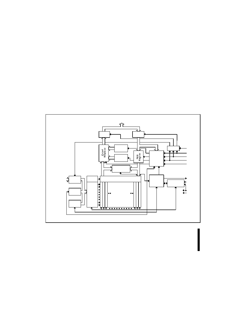
4-Mbit: A - A ,
8-Mbit: A - A ,
16-Mbit: A - A
0
18
0
19
0
20
Input
Buffer
Output
Buffer
Identifier
Register
Status
Register
Command
Register
I/O Logic
Data
Comparator
Input
Buffer
Address
Latch
Address
Counter
Y
Decoder
X
Decoder
Y Gating
4-Mbit: Eight
8-Mbit: Sixteen
16-Mbit: Thirty-Two
64-Kbyte Blocks
Write State
Machine
Program/Erase
Voltage Switch
CE#
WE#
OE#
RP#
RY/BY#
V
V
GND
DQ - DQ
PP
CC
V
CC
0
7
Figure 1. Block Diagram

E
28F004S3/28F008S3/28F016S3
7
PRELIMINARY
Table 1. Pin Descriptions
Sym
Type
Name and Function
A
0
≠A
20
INPUT
ADDRESS INPUTS: Inputs for addresses during read and write operations.
Addresses are internally latched during a write cycle.
4 Mbit
A
0
≠A
18
8 Mbit
A
0
≠A
19
16 Mbit
A
0
≠A
20
DQ
0
≠DQ
7
INPUT/
OUTPUT
DATA INPUT/OUTPUTS: Inputs data and commands during CUI write cycles;
outputs data during memory array, status register, and identifier code read cycles.
Data pins float to high-impedance when the chip is deselected or outputs are
disabled. Data is internally latched during a write cycle.
CE#
INPUT
CHIP ENABLE: Activates the device's control logic, input buffers, decoders, and
sense amplifiers. CE#-high deselects the device and reduces power consumption to
standby levels.
RP#
INPUT
RESET/DEEP POWER-DOWN: When driven low, RP# inhibits write operations
which provides data protection during power transitions, puts the device in deep
power-down mode, and resets internal automation. RP#-high enables normal
operation. Exit from deep power-down sets the device to read array mode.
RP# at V
HH
enables setting of the master lock-bit and enables configuration of block
lock-bits when the master lock-bit is set. RP# = V
HH
overrides block lock-bits,
thereby enabling block erase and program operations to locked memory blocks.
Block erase, program, or lock-bit configuration with V
IH
< RP# < V
HH
produce
spurious results and should not be attempted.
OE#
INPUT
OUTPUT ENABLE: Gates the device's outputs during a read cycle.
WE#
INPUT
WRITE ENABLE: Controls writes to the CUI and array blocks. Addresses and data
are latched on the rising edge of the WE# pulse.
RY/BY#
OUTPUT READY/BUSY#: Indicates the status of the internal WSM. When low, the WSM is
performing an internal operation (block erase, program, or lock-bit). RY/BY#-high
indicates that the WSM is ready for new commands, block erase or program is
suspended, or the device is in deep power-down mode. RY/BY# is always active.
V
PP
SUPPLY BLOCK ERASE, PROGRAM, LOCK-BIT CONFIGURATION POWER SUPPLY:
For erasing array blocks, programming data, or configuring lock-bits.
3 Volt Flash
2.7 V, 3.3 V and 12 V V
PP
With V
PP
V
PPLK
, memory contents cannot be altered. Block erase, program, and
lock-bit configuration with an invalid V
PP
(see
DC Characteristics) produce spurious
results and should not be attempted.
V
CC
SUPPLY DEVICE POWER SUPPLY: Internal detection automatically configures the device
for optimized read performance. Do not float any power pins.
3 Volt Flash
2.7 V and 3.3 V V
CC
With V
CC
V
LKO
, all write attempts to the flash memory are inhibited. Device
operations at invalid V
CC
voltages (see
DC Characteristics) produce spurious
results and should not be attempted. Block erase, program, and lock-bit
configuration operations with V
CC
< 2.7 V are not supported.
GND
SUPPLY GROUND: Do not float any ground pins.
NC
NO CONNECT: Lead is not internally connected; it may be driven or floated.
28F004S3/28F008S3/28F016S3
E
8
PRELIMINARY
28F004S3
28F008S3
28F016S3
NC
CE#
RP#
A
18
A
13
A
17
A
14
A
16
A
15
A
12
A
11
A
10
A
9
A
8
A
7
A
6
A
5
A
4
V
CC
V
PP
NC
WE#
OE#
RY/BY#
GND
GND
DQ
6
DQ
7
DQ
5
A
0
A
1
A
2
A
3
DQ
3
DQ
2
DQ
1
DQ
0
NC
V
CC
A
19
A
19
DQ
4
A
20
40-LEAD TSOP
STANDARD PINOUT
10 mm x 20 mm
TOP VIEW
1
2
3
4
5
6
7
8
9
10
11
12
13
14
15
16
17
18
19
20
21
22
23
24
25
26
27
28
29
30
31
32
40
39
38
37
36
35
34
33
CE#
RP#
A
18
A
13
A
17
A
14
A
16
A
15
A
12
A
11
A
10
A
9
A
8
A
7
A
6
A
5
A
4
V
CC
V
PP
CE#
RP#
A
18
A
13
A
17
A
14
A
16
A
15
A
12
A
11
A
10
A
9
A
8
A
7
A
6
A
5
A
4
V
CC
V
PP
NC
WE#
OE#
RY/BY#
GND
GND
DQ
6
DQ
7
DQ
5
A
0
A
1
A
2
A
3
DQ
3
DQ
2
DQ
1
DQ
0
NC
V
CC
DQ
4
NC
WE#
OE#
RY/BY#
GND
GND
DQ
6
DQ
7
DQ
5
A
0
A
1
A
2
A
3
DQ
3
DQ
2
DQ
1
DQ
0
V
CC
DQ
4
Figure 2. TSOP 40-Lead Pinout

E
28F004S3/28F008S3/28F016S3
9
PRELIMINARY
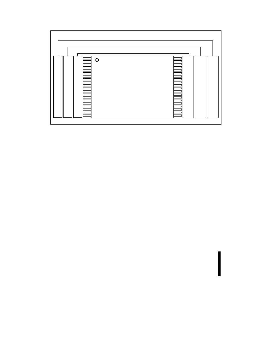
Figure 3. PSOP 44-Lead Pinout
28F004S3/28F008S3/28F016S3
E
10
PRELIMINARY
A
9
A
7
RP#
V
PP
V
CC
A
12
A
17
A
18
A
16
A
14
CE#
A
13
A
11
A
10
A
6
A
4
RY/BY#
A
3
NC
A
8
A
19
A
5
A
20
A
2
A
0
D
4
D
3
GND
D
1
D
6
WE#
OE#
D
7
D
2
V
CC
GND
D
5
D
0
A
1
A
15
8
7
6
5
4
3
2
1
A
B
C
D
E
A
B
C
D
E
A
15
A
17
A
12
V
CC
V
PP
RP#
A
7
A
6
A
10
A
11
CE#
A
13
A
14
A
16
A
18
NC
RY/BY#
A
19
NC
A
8
A
3
A
5
A
4
A
2
A
0
D
1
D
3
GND
D
4
D
6
WE#
OE#
D
7
D
5
V
CC
GND
D
2
D
0
A
1
A
9
1
2
3
4
5
6
7
8
Pin #1
Indicator
Top View - Bump Side Down
Bottom View - Bump Side Up
This is the view of the package as surface mounted on the board.
Note that the signals are mirror images of bottom view.
NOTES:
1.
Figures are not drawn to scale.
2.
Address A
20
is not included in the 28F008S3.
3.
More information on µBGA* packages is available by contacting your Intel/Distribution sales office.
Figure 4. µBGA* CSP 40-Bump Pinout (28F008S3 and 28F016S3)
E
28F004S3/28F008S3/28F016S3
11
PRELIMINARY
2.0
PRINCIPLES OF OPERATION
The 3 Volt FlashFile memories include an on-chip
WSM to manage block erase, program, and lock-bit
configuration functions. It allows for: 100% TTL-
level control inputs, fixed power supplies during
block erasure, program, and lock-bit configuration,
and minimal processor overhead with RAM-like
interface timings.
After initial device power-up or return from deep
power-down mode (see
Bus Operations), the
device defaults to read array mode. Manipulation of
external memory control pins allow array read,
standby, and output disable operations.
Status register and identifier codes can be
accessed through the CUI independent of the V
PP
voltage. High voltage on V
PP
enables successful
block erasure, program, and lock-bit configuration.
All functions associated with altering memory
contents--block erase, program, lock-bit
configuration, status, and identifier codes--are
accessed via the CUI and verified through the
status register.
Commands are written using standard micro-
processor write timings. The CUI contents serve as
input to the WSM that controls block erase,
program, and lock-bit configuration operations. The
internal algorithms are regulated by the WSM,
including pulse repetition, internal verification, and
margining of data. Addresses and data are
internally latched during write cycles. Writing the
appropriate command outputs array data, accesses
the identifier codes, or outputs status register data.
Interface software that initiates and polls progress
of block erase, program, and lock-bit configuration
can be stored in any block. This code is copied to
and executed from system RAM during flash
memory updates. After successful completion,
reads are again possible via the Read Array
command. Block erase suspend allows system
software to suspend a block erase to read data
from or program data to any other block. Program
suspend allows system software to suspend a
program to read data from any other flash memory
array location.
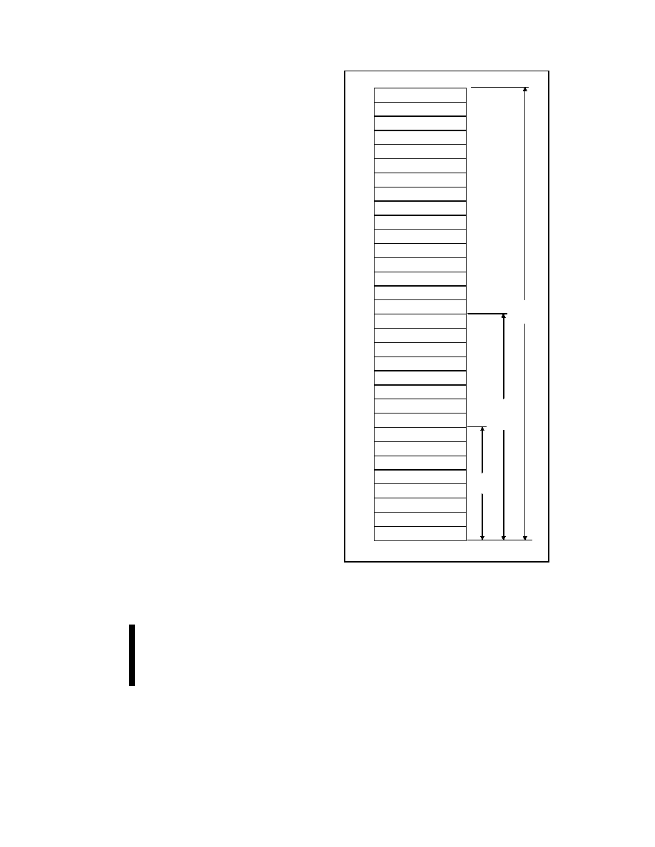
64-Kbyte Block
1FFFFF
31
1F0000
1EFFFF
1E0000
1DFFFF
1D0000
1CFFFF
1C0000
1BFFFF
30
29
28
27
1B0000
1AFFFF
1A0000
19FFFF
190000
18FFFF
180000
17FFFF
26
25
24
23
170000
16FFFF
160000
15FFFF
150000
14FFFF
140000
13FFFF
22
21
20
19
130000
12FFFF
120000
11FFFF
110000
10FFFF
100000
0FFFFF
18
17
16
15
0F0000
0EFFFF
0E0000
0DFFFF
0D0000
0CFFFF
0C0000
0BFFFF
14
13
12
11
0B0000
0AFFFF
0A0000
09FFFF
090000
08FFFF
080000
07FFFF
10
9
8
7
070000
06FFFF
060000
05FFFF
050000
04FFFF
040000
03FFFF
6
5
4
3
030000
02FFFF
020000
01FFFF
010000
00FFFF
000000
2
1
0
64-Kbyte Block
64-Kbyte Block
64-Kbyte Block
64-Kbyte Block
64-Kbyte Block
64-Kbyte Block
64-Kbyte Block
64-Kbyte Block
64-Kbyte Block
64-Kbyte Block
64-Kbyte Block
64-Kbyte Block
64-Kbyte Block
64-Kbyte Block
64-Kbyte Block
64-Kbyte Block
64-Kbyte Block
64-Kbyte Block
64-Kbyte Block
64-Kbyte Block
64-Kbyte Block
64-Kbyte Block
64-Kbyte Block
64-Kbyte Block
64-Kbyte Block
64-Kbyte Block
64-Kbyte Block
64-Kbyte Block
64-Kbyte Block
64-Kbyte Block
64-Kbyte Block
8-Mbit
16-Mbit
4-Mbit
Figure 5. Memory Map

28F004S3/28F008S3/28F016S3
E
12
PRELIMINARY
2.1
Data Protection
Depending on the application, the system designer
may choose to make the V
PP
power supply
switchable (available only when memory block
erase, program, or lock-bit configuration operations
are required) or hardwired to V
PPH1/2
. The device
accommodates either design practice and
encourages optimization of the processor-memory
interface.
When V
PP
V
PPLK
, memory contents cannot be
altered. When high voltage is applied to V
PP
, the
two-step block erase, program, or lock-bit
configuration command sequences provides pro-
tection from unwanted operations. All write
functions are disabled when V
CC
voltage is below
the write lockout voltage V
LKO
or when RP# is at
V
IL
. The device's block locking capability provides
additional protection from inadvertent code or data
alteration by gating erase and program operations.
3.0
BUS OPERATION
The local CPU reads and writes flash memory
in-system. All bus cycles to or from the flash
memory conform to standard microprocessor bus
cycles.
3.1
Read
Block information, identifier codes, or status register
can be read independent of the V
PP
voltage. RP#
can be at either V
IH
or V
HH
.
The first task is to write the appropriate read-mode
command (Read Array, Read Identifier Codes, or
Read Status Register) to the CUI. Upon initial
device power-up or after exit from deep power-
down mode, the device automatically resets to read
array mode. Four control pins dictate the data flow
in and out of the component: CE#, OE#, WE#, and
RP#. CE# and OE# must be driven active to obtain
data at the outputs. CE# is the device selection
control, and when active enables the selected
memory device. OE# is the data output (DQ
0
≠DQ
7
)
control and when active drives the selected
memory data onto the I/O bus. WE# must be at V
IH
and RP# must be at V
IH
or V
HH
. Figure 15
illustrates a read cycle.
3.2
Output Disable
With OE# at a logic-high level (V
IH
), the device
outputs are disabled. Output pins DQ
0
≠DQ
7
are
placed in a high-impedance state.
3.3
Standby
CE# at a logic-high level (V
IH
) places the device in
standby mode which substantially reduces device
power consumption. DQ
0
≠DQ
7
outputs are placed
in a high-impedance state independent of OE#. If
deselected during block erase, program, or lock-bit
configuration, the device continues functioning and
consuming active power until the operation
completes.
3.4
Deep Power-Down
RP# at V
IL
initiates the deep power-down mode.
In read mode, RP#-low deselects the memory,
places output drivers in a high-impedance state,
and turns off all internal circuits. RP# must be held
low for time t
PLPH
. Time t
PHQV
is required after
return from power-down until initial memory access
outputs are valid. After this wake-up interval,
normal operation is restored. The CUI resets to
read array mode, and the status register is set to
80H.
During block erase, program, or lock-bit
configuration, RP#-low will abort the operation.
RY/BY# remains low until the reset operation is
complete. Memory contents being altered are no
longer valid; the data may be partially erased or
written. Time t
PHWL
is required after RP# goes to
logic-high (V
IH
) before another command can be
written.
As with any automated device, it is important to
assert RP# during system reset. When the system
comes out of reset, it expects to read from the flash
memory. Automated flash memories provide status
information when accessed during block erase,
program, or lock-bit configuration modes. If a CPU
reset occurs with no flash memory reset, proper
CPU initialization may not occur because the flash
memory may be providing status information
instead of array data. Intel's flash memories allow
proper CPU initialization following a system reset
through the use of the RP# input. In this application,
RP# is controlled by the same RESET# signal that
resets the system CPU.
E
28F004S3/28F008S3/28F016S3
13
PRELIMINARY
000000
Block 0
Master Lock Configuration
000001
000002
000003
010000
010002
00FFFF
Device Code
Block 0 Lock Configuration
Manufacturer Code
Reserved For
Future Implementation
Block 1
Block 1 Lock Configuration
Reserved for
Future Implementation
01FFFF
Reserved for
Future Implementation
1F0000
1F0002
Block 31 Lock Configuration
Reserved for
Future Implementation
1FFFFF
Block 31
(Blocks 16 through 30)
(Blocks 8 through 14)
(Blocks 2 through 14)
070000
070002
Block 7
Block 7 Lock Configuration
Reserved for
Future Implementation
07FFFF
Reserved for
Future Implementation
0F0000
0F0002
Block 15
Block 15 Lock Configuration
Reserved for
Future Implementation
0FFFFF
8-Mbit
16-Mbit
4-Mbit
Reserved for
Future Implementation
Reserved for
Future Implementation
Figure 6. Device Identifier Code Memory Map
3.5
Read Identifier Codes
Operation
The read identifier codes operation outputs the
manufacturer code, device code, block lock
configuration codes for each block, and master lock
configuration code (see Figure 6). Using the
manufacturer and device codes, the system
software can automatically match the device with its
proper algorithms. The block lock and master lock
configuration codes identify locked and unlocked
blocks and master lock-bit setting.
3.6
Write
The CUI does not occupy an addressable memory
location. It is written when WE# and CE# are active
and OE# = V
IH
. The address and data needed to
execute a command are latched on the rising edge
of WE# or CE# (whichever goes high first).
Standard microprocessor write timings are used.
Figure 18 illustrates a write operation.
4.0
COMMAND DEFINITIONS
When the V
PP
voltage
V
PPLK
, read operations
from the status register, identifier codes, or blocks
are enabled. Placing V
PPH1/2
on V
PP
enables
successful block erase, program, and lock-bit
configuration operations.
Device operations are selected by writing specific
commands into the CUI. Table 3 defines these
commands.

28F004S3/28F008S3/28F016S3
E
14
PRELIMINARY
Table 2. Bus Operations
Mode
Notes
RP#
CE#
OE#
WE#
Address
V
PP
DQ
0≠7
RY/BY#
Read
1,2,3
V
IH
or
V
HH
V
IL
V
IL
V
IH
X
X
D
OUT
X
Output Disable
3
V
IH
or
V
HH
V
IL
V
IH
V
IH
X
X
High Z
X
Standby
3
V
IH
or
V
HH
V
IH
X
X
X
X
High Z
X
Deep Power-Down
4
V
IL
X
X
X
X
X
High Z
V
OH
Read Identifier Codes
V
IH
or
V
HH
V
IL
V
IL
V
IH
See
Figure 5
X
Note 5
V
OH
Write
3,6,7
V
IH
or
V
HH
V
IL
V
IH
V
IL
X
X
D
IN
X
NOTES:
1. Refer to
DC Characteristics. When V
PP
V
PPLK
, memory contents can be read, but not altered.
2. X can be V
IL
or V
IH
for control and address input pins and V
PPLK
or V
PPH1/2
for V
PP
. See
DC Characteristics for V
PPLK
and
V
PPH1/2
voltages.
3. RY/BY# is V
OL
when the WSM is executing internal block erase, program, or lock-bit configuration algorithms. It is V
OH
when the WSM is not busy, in block erase suspend, program suspend, or deep power-down mode.
4. RP# at GND ± 0.2 V ensures the lowest deep power-down current.
5. See Section 4.2 for read identifier code data.
6. Command writes involving block erase, program, or lock-bit configuration are reliably executed when V
PP
= V
PPH1/2
and
V
CC
= V
CC2
(see Section 6.2 for operating conditions).
7. Refer to Table 3 for valid D
IN
during a write operation.

E
28F004S3/28F008S3/28F016S3
15
PRELIMINARY
Table 3. Command Definitions
(9)
Bus Cycles
First Bus Cycle
Second Bus Cycle
Command
Req'd.
Notes
Oper
(1)
Addr
(2)
Data
(3)
Oper
(1)
Addr
(2)
Data
(3)
Read Array/Reset
1
Write
X
FFH
Read Identifier Codes
2
4
Write
X
90H
Read
IA
ID
Read Status Register
2
Write
X
70H
Read
X
SRD
Clear Status Register
1
Write
X
50H
Block Erase
2
5
Write
BA
20H
Write
BA
D0H
Program
2
5,6
Write
PA
40H
or
10H
Write
PA
PD
Block Erase and Program
Suspend
1
5
Write
X
B0H
Block Erase and Program
Resume
1
5
Write
X
D0H
Set Block Lock-Bit
2
7
Write
BA
60H
Write
BA
01H
Set Master Lock-Bit
2
7
Write
X
60H
Write
X
F1H
Clear Block Lock-Bits
2
8
Write
X
60H
Write
X
D0H
NOTES:
1. Bus operations are defined in Table 2.
2. X = Any valid address within the device.
IA = Identifier Code Address: see Figure 6.
BA = Address within the block being erased or locked.
PA = Address of memory location to be programmed.
3. SRD = Data read from status register. See Table 6 for a description of the status register bits.
PD = Data to be programmed at location PA. Data is latched on the rising edge of WE# or CE# (whichever goes high first).
ID = Data read from identifier codes.
4. Following the Read Identifier Codes command, read operations access manufacturer, device, block lock, and master lock
codes. See Section 4.2 for read identifier code data.
5. If the block is locked, RP# must be at V
HH
to enable block erase or program operations. Attempts to issue a block erase or
program to a locked block while RP# is V
IH
will fail.
6. Either 40H or 10H are recognized by the WSM as the program setup.
7. If the master lock-bit is set, RP# must be at V
HH
to set a block lock-bit. RP# must be at V
HH
to set the master lock-bit. If the
master lock-bit is not set, a block lock-bit can be set while RP# is V
IH
.
8. If the master lock-bit is set, RP# must be at V
HH
to clear block lock-bits. The clear block lock-bits operation simultaneously
clears all block lock-bits. If the master lock-bit is not set, the Clear Block Lock-Bits command can be done while RP# is V
IH
.
9. Commands other than those shown above are reserved by Intel for future device implementations and should not be used.
28F004S3/28F008S3/28F016S3
E
16
PRELIMINARY
4.1
Read Array Command
Upon initial device power-up and after exit from
deep power-down mode, the device defaults to read
array mode. This operation is also initiated by
writing the Read Array command. The device
remains enabled for reads until another command
is written. Once the internal WSM has started a
block erase, program, or lock-bit configuration, the
device will not recognize the Read Array command
until the WSM completes its operation unless the
WSM is suspended via an Erase Suspend or
Program Suspend command. The Read Array
command functions independently of the V
PP
voltage and RP# can be V
IH
or V
HH
.
4.2
Read Identifier Codes
Command
The identifier code operation is initiated by writing
the Read Identifier Codes command. Following the
command write, read cycles from addresses shown
in Figure 6 retrieve the manufacturer, device, block
lock configuration and master lock configuration
codes (see Table 4 for identifier code values). To
terminate the operation, write another valid
command. Like the Read Array command, the
Read Identifier Codes command functions
independently of the V
PP
voltage and RP# can be
V
IH
or V
HH
. Following the Read Identifier Codes
command, the subsequent information can be read.
Table 4. Identifier Codes
Code
Address
Data
Manufacturer Code
000000
89
4-Mbit
000001
A7
Device Code
8-Mbit
000001
A6
16-Mbit
000001
AA
Block Lock Configuration
XX
0002
(1)
∑
Block Is Unlocked
DQ
0
= 0
∑
Block Is Locked
DQ
0
= 1
∑
Reserved for Future Use
DQ
1≠7
Master Lock Configuration
000003
∑
Device Is Unlocked
DQ
0
= 0
∑
Device Is Locked
DQ
0
= 1
∑
Reserved for Future Use
DQ
1≠7
NOTE:
1.
X selects the specific block lock configuration code to
be read. See Figure 5 for the device identifier code
memory map.
4.3
Read Status Register
Command
The status register may be read to determine when
a block erase, program, or lock-bit configuration is
complete and whether the operation completed
successfully. It may be read at any time by writing
the Read Status Register command. After writing
this command, all subsequent read operations
output data from the status register until another
valid command is written. The status register
contents are latched on the falling edge of OE# or
CE#, whichever occurs first. OE# or CE# must
toggle to V
IH
to update the status register latch. The
Read Status Register command functions
independently of the V
PP
voltage. RP# can be V
IH
or V
HH
.
4.4
Clear Status Register
Command
Status register bits SR.5, SR.4, SR.3, and SR.1 are
set to "1"s by the WSM and can only be reset by
the Clear Status Register command. These bits
indicate various failure conditions (see Table 6). By
allowing system software to reset these bits,
several operations (such as cumulatively erasing or
locking multiple blocks or writing several bytes in
sequence) may be performed. The status register
may be polled to determine if an error occurred
during the sequence.
To clear the status register, the Clear Status
Register command (50H) is written. It functions
independently of the applied V
PP
voltage. RP# can
be V
IH
or V
HH
. This command is not functional
during block erase or program suspend modes.
4.5
Block Erase Command
Erase is executed one block at a time and initiated
by a two-cycle command. A block erase setup is
written first, followed by a block erase confirm. This
command sequence requires appropriate se-
quencing and an address within the block to be
erased (erase changes all block data to FFH).
Block preconditioning, erase, and verify are handled
internally by the WSM (invisible to the system).
After the two-cycle block erase sequence is written,
the device automatically outputs status register
data when read (see Figure 7). The CPU can detect
block erase completion by analyzing the RY/BY#
pin or status register bit SR.7.

E
28F004S3/28F008S3/28F016S3
17
PRELIMINARY
When the block erase is complete, status register
bit SR.5 should be checked. If a block erase error is
detected, the status register should be cleared
before system software attempts corrective actions.
The CUI remains in read status register mode until
a new command is issued.
This two-step command sequence of set-up
followed by execution ensures that block contents
are not accidentally erased. An invalid Block Erase
command sequence will result in both status
register bits SR.4 and SR.5 being set to "1." Also,
reliable block erasure can only occur when
V
CC
= V
CC2
and V
PP
= V
PPH1/2
. In the absence of
this high voltage, block contents are protected
against erasure. If block erase is attempted while
V
PP
V
PPLK
, SR.3 and SR.5 will be set to "1."
Successful block erase requires that the
corresponding block lock-bit be cleared or, if set,
that RP# = V
HH
. If block erase is attempted when
the corresponding block lock-bit is set and
RP# = V
IH
, the block erase will fail, and SR.1 and
SR.5 will be set to "1." Block erase operations with
V
IH
< RP# < V
HH
produce spurious results and
should not be attempted.
4.6
Program Command
Program is executed by a two-cycle command
sequence. Program setup (standard 40H or
alternate 10H) is written, followed by a second write
that specifies the address and data (latched on the
rising edge of WE#). The WSM then takes over,
controlling the program and verify algorithms
internally. After the program sequence is written,
the device automatically outputs status register
data when read (see Figure 8). The CPU can detect
the completion of the program event by analyzing
the RY/BY# pin or status register bit SR.7.
When program is complete, status register bit SR.4
should be checked. If program error is detected, the
status register should be cleared. The internal WSM
verify only detects errors for "1"s that do not
successfully program to "0"s. The CUI remains in
read status register mode until it receives another
command.
Reliable program only occurs when V
CC
= V
CC2
and
V
PP
= V
PPH1/2
. In the absence of this high voltage,
memory contents are protected against program
operations. If a program operation is attempted
while V
PP
V
PPLK
, the operation will fail, and status
register bits SR.3 and SR.5 will be set to "1."
A successful program operation also requires that
the corresponding block lock-bit be cleared or, if
set, that RP# = V
HH
. If a program operation is
attempted when the corresponding block lock-bit is
set and RP# = V
IH
, the operation will fail, and SR.1
and SR.4 will be set to "1." Program operations with
V
IH
< RP# < V
HH
produce spurious results and
should not be attempted.
4.7
Block Erase Suspend
Command
The Block Erase Suspend command allows
block-erase interruption to read or program data in
another block of memory. Once the block erase
process starts, writing the Block Erase Suspend
command requests that the WSM suspend the
block erase sequence at a predetermined point in
the algorithm. The device outputs status register
data when read after the Block Erase Suspend
command is written. Polling status register bits
SR.7 and SR.6 can determine when the block erase
operation has been suspended (both will be set to
"1"). RY/BY# will also transition to V
OH
.
Specification t
WHRH2
defines the block erase
suspend latency.
At this point, a Read Array command can be written
to read data from blocks other than that which is
suspended. A Program command sequence can
also be issued during erase suspend to program
data in other blocks. Using the Program Suspend
command (see Section 4.8), a program operation
can also be suspended. During a program operation
with block erase suspended, status register bit
SR.7 will return to "0" and the RY/BY# output will
transition to V
OL
. However, SR.6 will remain "1" to
indicate block erase suspend status.
The only other valid commands while block erase is
suspended are Read Status Register and Block
Erase Resume. After a Block Erase Resume
command is written to the flash memory, the WSM
will continue the block erase process. Status
register bits SR.6 and SR.7 will automatically clear
and RY/BY# will return to V
OL
. After the Erase
Resume command is written, the device
automatically outputs status register data when
read (see Figure 9). V
PP
must remain at V
PPH1/2
(the same V
PP
level used for block erase) while
block erase is suspended. RP# must also remain at
V
IH
or V
HH
(the same RP# level used for block
erase). Block erase cannot resume until program
operations initiated during block erase suspend
have completed.

28F004S3/28F008S3/28F016S3
E
18
PRELIMINARY
4.8
Program Suspend Command
The Program Suspend command allows program
interruption to read data in other flash memory
locations. Once the program process starts, writing
the Program Suspend command requests that the
WSM suspend the program sequence at a
predetermined point in the algorithm. The device
continues to output status register data when read
after the Program Suspend command is written.
Polling status register bits SR.7 and SR.2 can
determine when the program operation has been
suspended (both will be set to "1"). RY/BY# will also
transition to V
OH
. Specification t
WHRH1
defines the
program suspend latency.
At this point, a Read Array command can be written
to read data from locations other than that which is
suspended. The only other valid commands while
program is suspended are Read Status Register
and Program Resume. After Program Resume
command is written to the flash memory, the WSM
will continue the program process. Status register
bits SR.2 and SR.7 will automatically clear and
RY/BY# will return to V
OL
. After the Program
Resume command is written, the device
automatically outputs status register data when
read (see Figure 10). V
PP
must remain at V
PPH1/2
(the same V
PP
level used for program) while in
program suspend mode. RP# must also remain at
V
IH
or V
HH
(the same RP# level used for program).
4.9
Set Block and Master Lock-Bit
Commands
A flexible block locking and unlocking scheme is
enabled via a combination of block lock-bits and a
master lock-bit. The block lock-bits gate program
and erase operations while the master lock-bit
gates block-lock bit modification. With the master
lock-bit not set, individual block lock-bits can be set
using the Set Block Lock-Bit command. The Set
Master Lock-Bit command, in conjunction with
RP# = V
HH
, sets the master lock-bit. After the
master lock-bit is set, subsequent setting of block
lock-bits requires both the Set Block Lock-Bit
command and V
HH
on the RP# pin. See Table 5 for
a summary of hardware and software write
protection options.
Set block lock-bit and master lock-bit are initiated
using two-cycle command sequence. The set block
or master lock-bit setup along with appropriate
block or device address is written followed by either
the set block lock-bit confirm (and an address within
the block to be locked) or the set master lock-bit
confirm (and any device address). The WSM then
controls the set lock-bit algorithm. After the
sequence is written, the device automatically
outputs status register data when read (see
Figure 11). The CPU can detect the completion of
the set lock-bit event by analyzing the RY/BY# pin
output or status register bit SR.7.
When the set lock-bit operation is complete, status
register bit SR.4 should be checked. If an error is
detected, the status register should be cleared. The
CUI will remain in read status register mode until a
new command is issued.
This two-step sequence of setup followed by
execution ensures that lock-bits are not accidentally
set. An invalid Set Block or Master Lock-Bit
command will result in status register bits SR.4 and
SR.5 being set to "1." Also, reliable operations
occur only when V
CC
= V
CC2
and V
PP
= V
PPH1/2
. In
the absence of this high voltage, lock-bit contents
are protected against alteration.
A successful set block lock-bit operation requires
that the master lock-bit be cleared or, if the master
lock-bit is set, that RP# = V
HH
. If it is attempted with
the master lock-bit set and RP# = V
IH
, the operation
will fail, and SR.1 and SR.4 will be set to "1." A
successful set master lock-bit operation requires
that RP# = V
HH
. If it is attempted with RP# = V
IH
,
the operation will fail, and SR.1 and SR.4 will be set
to "1." Set block and master lock-bit operations with
V
IH
< RP# < V
HH
produce spurious results and
should not be attempted.

E
28F004S3/28F008S3/28F016S3
19
PRELIMINARY
4.10
Clear Block Lock-Bits
Command
All set block lock-bits are cleared in parallel via the
Clear Block Lock-Bits command. With the master
lock-bit not set, block lock-bits can be cleared using
only the Clear Block Lock-Bits command. If the
master lock-bit is set, clearing block lock-bits
requires both the Clear Block Lock-Bits command
and V
HH
on the RP# pin. See Table
5 for a
summary of hardware and software write protection
options.
Clear block lock-bits operation is initiated using a
two-cycle command sequence. A clear block
lock-bits setup is written first. Then, the device
automatically outputs status register data when
read (see Figure 12). The CPU can detect
completion of the clear block lock-bits event by
analyzing the RY/BY# pin output or status register
bit SR.7.
When the operation is complete, status register bit
SR.5 should be checked. If a clear block lock-bit
error is detected, the status register should be
cleared. The CUI will remain in read status register
mode until another command is issued.
This two-step sequence of set-up followed by
execution ensures that block lock-bits are not
accidentally cleared. An invalid Clear Block
Lock-Bits command sequence will result in status
register bits SR.4 and SR.5 being set to "1." Also, a
reliable clear block lock-bits operation can only
occur when V
CC
= V
CC2
and V
PP
= V
PPH1/2
. If a
clear block lock-bits operation is attempted while
V
PP
V
PPLK
, SR.3 and SR.5 will be set to "1." In the
absence of this high voltage, the block lock-bits
content are protected against alteration. A suc-
cessful clear block lock-bits operation requires that
the master lock-bit is not set or, if the master lock-
bit is set, that RP# = V
HH
. If it is attempted with the
master lock-bit set and RP# = V
IH
, SR.1 and SR.5
will be set to "1" and the operation will fail. A clear
block lock-bits operation with V
IH
< RP# < V
HH
produce spurious results and should not be
attempted.
If a clear block lock-bits operation is aborted due to
V
PP
or V
CC
transitioning out of valid range or RP#
active transition, block lock-bit values are left in an
undetermined state. A repeat of clear block lock-
bits is required to initialize block lock-bit contents to
known values. Once the master lock-bit is set, it
cannot be cleared.
Table 5. Write Protection Alternatives
Operation
Master
Lock-Bit
Block
Lock-Bit
RP#
Effect
Block Erase or
0
V
IH
or V
HH
Block Erase and Program Enabled
Byte Write
X
1
V
IH
Block is Locked. Block Erase and Program Disabled
V
HH
Block Lock-Bit Override. Block Erase and Program
Enabled
Set Block
0
X
V
IH
or V
HH
Set Block Lock-Bit Enabled
Lock-Bit
1
X
V
IH
Master Lock-Bit is Set. Set Block Lock-Bit Disabled
V
HH
Master Lock-Bit Override. Set Block Lock-Bit
Enabled
Set Master
X
X
V
IH
Set Master Lock-Bit Disabled
Lock-Bit
V
HH
Set Master Lock-Bit Enabled
Clear Block
0
X
V
IH
or V
HH
Clear Block Lock-Bits Enabled
Lock-Bits
1
X
V
IH
Master Lock-Bit is Set. Clear Block Lock-Bits
Disabled
V
HH
Master Lock-Bit Override. Clear Block Lock-Bits
Enabled
28F004S3/28F008S3/28F016S3
E
20
PRELIMINARY
Table 6. Status Register Definition
WSMS
ESS
ECLBS
PSLBS
VPPS
PSS
DPS
R
7
6
5
4
3
2
1
0
NOTES:
SR.7 = WRITE STATE MACHINE STATUS
1 = Ready
0 = Busy
Check RY/BY# or SR.7 to determine block erase,
program, or lock-bit configuration completion.
SR.6≠0 are invalid while SR.7 = "0."
SR.6 = ERASE SUSPEND STATUS
1 = Block Erase Suspended
0 = Block Erase in Progress/Completed
SR.5 = ERASE AND CLEAR LOCK-BITS
STATUS
1 = Error in Block Erasure or Clear Lock-Bits
0 = Successful Block Erase or Clear Lock-Bits
If both SR.5 and SR.4 are "1"s after a block erase or
lock-bit configuration attempt, an improper
command sequence was entered.
SR.4 = PROGRAM AND SET LOCK-BIT
STATUS
1 = Error in Program or Set Master/Block
Lock-Bit
0 = Successful Program or Set Master/Block
Lock-Bit
SR.3 = V
PP
STATUS
1 = V
PP
Low Detect, Operation Abort
0 = V
PP
OK
SR.3 does not provide a continuous indication of
V
PP
level. The WSM interrogates and indicates the
V
PP
level only after a block erase, program, or lock-
bit configuration operation. SR.3 is not guaranteed
to reports accurate feedback only when V
PP
V
PPH1/2
.
SR.2 = PROGRAM SUSPEND STATUS
1 = Program Suspended
0 = Program in Progress/Completed
SR.1 = DEVICE PROTECT STATUS
1 = Master Lock-Bit, Block Lock-Bit and/or
RP# Lock Detected, Operation Abort
0 = Unlock
SR.1 does not provide a continuous indication of
master and block lock-bit values. The WSM
interrogates the master lock-bit, block lock-bit, and
RP# only after a block erase, program, or lock-bit
configuration operation. It informs the system,
depending on the attempted operation, if the block
lock-bit is set, master lock-bit is set, and/or
RP#
V
HH
.
SR.0 = RESERVED FOR FUTURE
ENHANCEMENTS
SR.0 is reserved for future use and should be
masked out when polling the status register.

E
28F004S3/28F008S3/28F016S3
21
PRELIMINARY
SR.7 =
0
1
Start
Write 20H,
Block Address
Write D0H,
Block Address
Full Status
Check if Desired
Block Erase
Complete
FULL STATUS CHECK PROCEDURE
1
0
Read Status Register
Data (See Above)
1
0
Read Status
Register
Suspend
Block Erase
Suspend Block
Erase Loop
Yes
No
1
0
Command Sequence
Error
SR.3 =
SR.5 =
SR.4,5 =
Block Erase
Error
Bus
Operation
Command
Comments
Standby
Check SR.4,5
Both 1 = Command Sequence Error
Standby
SR.5, SR.4, SR.3 and SR.1 are only cleared by the Clear Status
Register command in cases where multiple blocks are erased
before full status is checked.
If error is detected, clear the Status Register before attempting
retry or other error recovery.
Check SR.5
1 = Block Erase Error
Standby
Bus
Operation
Command
Comments
Write
Write
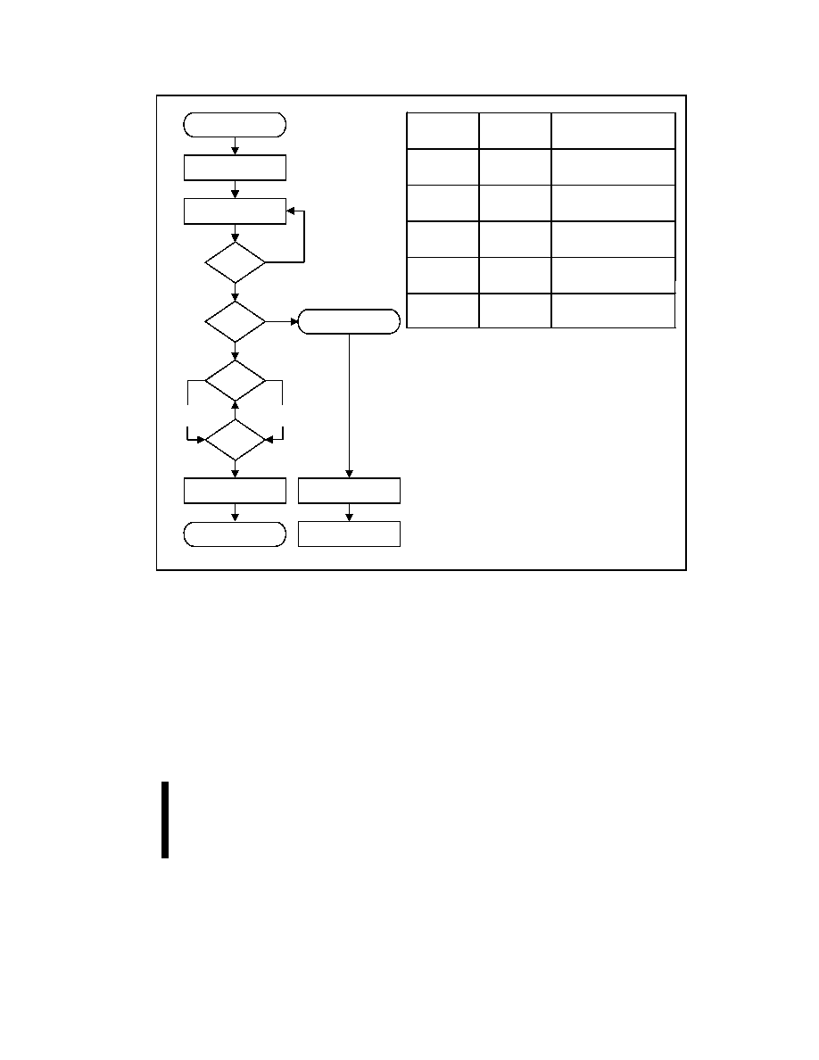
Erase Setup
Read
Data = 20H
Addr = Within Block to Be Erased
Check SR.7
1 = WSM Ready
0 = WSM Busy
Repeat for subsequent block erasures.
Full status check can be done after each block erase, or after a
sequence of block erasures.
Write FFH after the last operation to place device in read array mode.
Status Register Data
Standby
Erase
Confirm
Data = D0H
Addr = Within Block to Be Erased
Block Erase
Successful
Standby
Check SR.1
1 = Device Protect Detect
RP# = V , Block Lock-Bit Is Set
Only required for systems
implementing lock-bit configuration
0
1
Device Protect Error
SR.1 =
Check SR.3
1 = V Error Detect
PP
IH
V Range Error
PP
Figure 7. Automated Block Erase Flowchart
28F004S3/28F008S3/28F016S3
E
22
PRELIMINARY
SR.7 =
0
1
Start
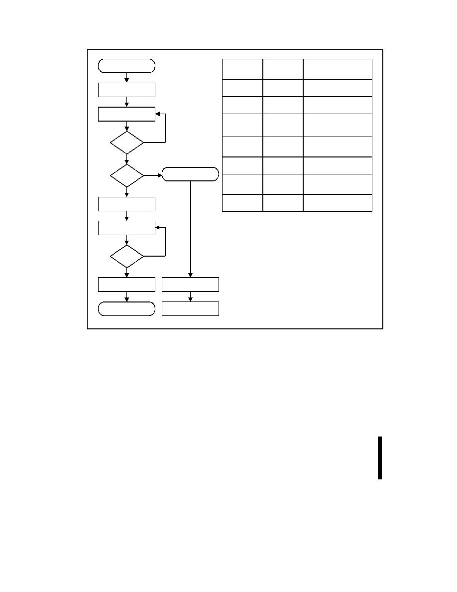
Write 40H,
Address
Write Byte
Data and Address
Full Status
Check if Desired
Program Complete
FULL STATUS CHECK PROCEDURE
1
0
Read Status Register
Data (See Above)
1
0
Read
Status Register
V Range Error
Bus
Operation
Command
Comments
Standby
Standby
Check SR.3
1 = V Error Detect
SR.4, SR.3 and SR.1 are only cleared by the Clear Status Register
command in cases where multiple locations are written before
full status is checked.
If error is detected, clear the Status Register before attempting
retry or other error recovery.
Bus
Operation
Command
Comments
Write
Write
Setup
Program
Data = Data to Be Programmed
Addr = Location to Be Programmed
Read
Data = 40H
Addr = Location to Be Programmed
Check SR.7
1 = WSM Ready
0 = WSM Busy
Repeat for subsequent byte writes.
SR full status check can be done after each program, or after a
sequence of program operations.
Write FFH after the last program operation to reset device to
read array mode.
Standby
SR.3 =
SR.4 =
Program Error
Program Successful
Program
Status Register Data
Suspend
Program
Yes
No
Suspend
Program Loop
Standby
Check SR.4
1 = Program Error
0
1
Device Protect Error
SR.1 =
PP
Check SR.1
1 = Device Protect Detect
RP# = V , Block Lock-Bit Is Set
Only required for systems
implementing lock-bit configuration
IH
PP
Figure 8. Automated Program Flowchart
E
28F004S3/28F008S3/28F016S3
23
PRELIMINARY
SR.7 =
0
1
Start
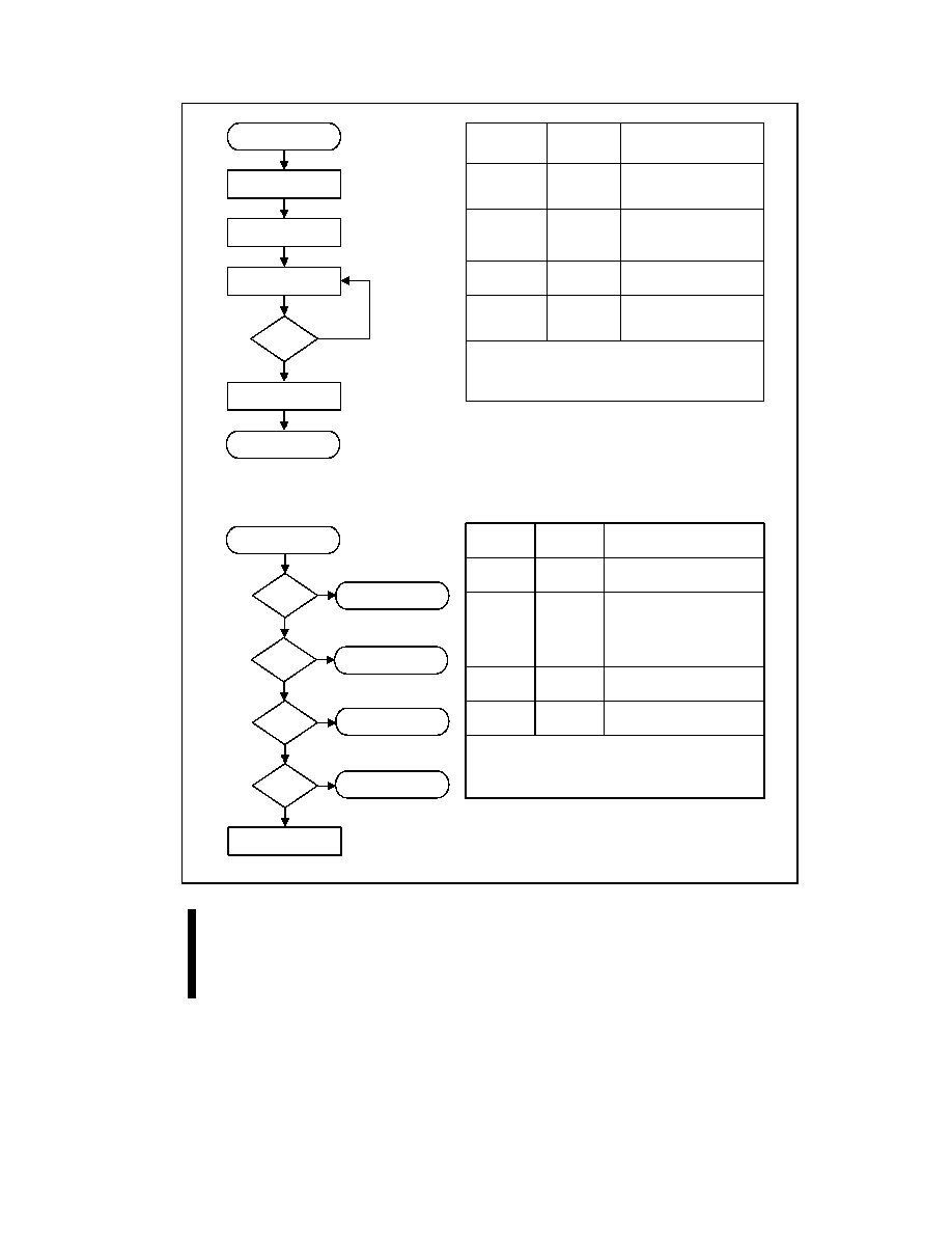
Write B0H
Read
Status Register
Write D0H
Block Erase Resumed
Bus
Operation
Command
Comments
Write
Erase
Suspend
Read
Data = B0H
Addr = X
Check SR.7
1 = WSM Ready
0 = WSM Busy
Status Register Data
Addr = X
Standby
SR.6 =
Block Erase Completed
Write FFH
Read Array Data
Yes
0
1
Check SR.6
1 = Block Erase Suspended
0 = Block Erase Completed
Standby
Data = D0H
Addr = X
Write
Erase
Resume
Read or
Program
?
Done?
Program
Loop
Read Array
Data
Read
Program
No
Figure 9. Block Erase Suspend/Resume Flowchart
28F004S3/28F008S3/28F016S3
E
24
PRELIMINARY
SR.7 =
0
1
Start
Write B0H
Read
Status Register
Write D0H
Program Resumed
Bus
Operation
Command
Comments
Write
Program
Suspend
Read
Data = B0H
Addr = X
Check SR.7
1 = WSM Ready
0 = WSM Busy
Status Register Data
Addr = X
Standby
SR.2 =
Write FFH
Read Array Data
Done
Reading
Program Completed
Write FFH
Read Array Data
Yes
No
0
1
Check SR.2
1 =Program Suspended
0 = Program Completed
Standby
Data = FFH
Addr = X
Write
Read array locations other
than that being data written.
Read
Data = D0H
Addr = X
Write
Read Array
Program
Resume
Figure 10. Program Suspend/Resume Flowchart
E
28F004S3/28F008S3/28F016S3
25
PRELIMINARY
SR.7 =
0
1
Start
Write 60H,
Block/Device Address
Write 01H/F1H,
Block/Device Address
Full Status
Check if Desired
Set Lock-Bit Complete
FULL STATUS CHECK PROCEDURE
1
0
Read Status Register
Data (See Above)
1
0
Read Status
Register
V Range Error
1
0
Command Sequence
Error
SR.3 =
SR.4 =
SR.4,5 =
Set Lock-Bit Error
Bus
Operation
Command
Comments
Standby
Check SR.4,5
Both 1 = Command Sequence Error
Standby
SR.5, SR.4, SR.3 and SR.1 are only cleared by the Clear Status
Register command in cases where multiple lock-bits are set before
full status is checked.
If error is detected, clear the Status Register before attempting retry
or other error recovery.
Check SR.4
1 = Set Lock-Bit Reset Error
Standby
Bus
Operation
Command
Comments
W rite
W rite
Set
Block/Master
Lock-Bit Setup
Read
Data = 60H
Addr = Block Address (Block),
Device Address (Master)
Check SR.7
1 = WSM Ready
0 = WSM Busy
Repeat for subsequent lock-bit set operations.
Full status check can be done after each lock-bit set operation or after
a sequence of lock-bit set operations.
Write FFH after the last lock-bit set operation to place device in
read array mode.
Status Register Data
Standby
Set
Block or Master
Lock-Bit Confirm
Data = 01H (Block),
F1H (Master)
Addr = Block Address (Block),
Device Address (Master)
Set Lock-Bit Successful
Standby
0
1
Device Protect Error
SR.1 =
Check SR.3
1 = V Error Detect
PP
PP
Check SR.1
1 = Device Protect Detect
RP# = V ,
(Set Master Lock-Bit Operation)
RP# = V , Master Lock-Bit Is Set
(Set Block Lock-Bit Operation)
IH
HH
Figure 11. Set Block and Master Lock-Bit Flowchart

28F004S3/28F008S3/28F016S3
E
26
PRELIMINARY
SR.7 =
0
1
Start
Write 60H
Write D0H
Full Status
Check if Desired
Clear Block Lock-Bits
Complete
FULL STATUS CHECK PROCEDURE
1
0
Read Status Register
Data (See Above)
1
0
Read Status
Register
V Range Error
1
0
Command Sequence
Error
SR.3 =
SR.5 =
SR.4,5 =
Clear Block Lock-Bits
Error
Bus
Operation
Command
Comments
Standby
Check SR.4,5
Both 1 = Command Sequence Error
Standby
SR.5, SR.4, SR.3 and SR.1 are only cleared by the Clear Status
Register command.
If error is detected, clear the Status Register before attempting
retry or other error recovery.
Check SR.5
1 = Clear Block Lock-Bits Error
Standby
Bus
Operation
Command
Comments
Write
Write
Clear Block
Lock-Bits Setup
Read
Data = 60H
Addr = X
Check SR.7
1 = WSM Ready
0 = WSM Busy
Write FFH after the Clear Block Lock-Bits operation to place device
to read array mode.
Status Register Data
Standby
Clear Block
Lock-Bits Confirm
Data = D0H
Addr = X
Clear Block Lock-Bits
Successful
Standby
0
1
Device Protect Error
SR.1=
Check SR.3
1 = V Error Detect
PP
PP
Check SR.1
1 = Device Protect Detect
RP# = V , Master Lock-Bit Is Set
IH
Figure 12. Clear Block Lock-Bits Flowchart

E
28F004S3/28F008S3/28F016S3
27
PRELIMINARY
5.0
DESIGN CONSIDERATIONS
5.1
Three-Line Output Control
Intel provides three control inputs to accommodate
multiple memory connections: CE#, OE#, and RP#.
Three-line control provides for:
a.
Lowest possible memory power dissipation.
b.
Data bus contention avoidance.
To use these control inputs efficiently, an address
decoder should enable CE# while OE# should be
connected to all memory devices and the system's
READ# control line. This assures that only selected
memory devices have active outputs while de-
selected memory devices are in standby mode.
RP# should be connected to the system
POWERGOOD signal to prevent unintended writes
during system power transitions. POWERGOOD
should also toggle during system reset.
5.2
RY/BY# Hardware Detection
RY/BY# is a full CMOS output that provides a
hardware method of detecting block erase program
and lock-bit configuration completion. This output
can be directly connected to an interrupt input of
the system CPU. RY/BY# transitions low when the
WSM is busy and returns to V
OH
when it is finished
executing the internal algorithm. During suspend
and deep power-down modes, RY/BY# remains at
V
OH
.
5.3
Power Supply Decoupling
Flash memory power switching characteristics
require careful device decoupling. System
designers are interested in three supply current
issues: standby current levels, active current levels
and transient peaks produced by falling and rising
edges of CE# and OE#. Two-line control and proper
decoupling capacitor selection will suppress
transient voltage peaks. Each device should have a
0.1 µF ceramic capacitor connected between its
V
CC
and GND and between its V
PP
and GND.
These high-frequency, low-inductance capacitors
should be placed as close as possible to package
leads. Additionally, for every eight devices, a 4.7 µF
electrolytic capacitor should be placed at the array's
power supply connection between V
CC
and GND.
The bulk capacitor will overcome voltage slumps
caused by PC board trace inductance.
5.4
V
PP
Trace on Printed Circuit
Boards
Updating flash memories that reside in the target
system requires that the printed circuit board
designer pay attention to the V
PP
power supply
trace. The V
PP
pin supplies the memory cell current
for byte writing and block erasing. Use similar trace
widths and layout considerations given to the V
CC
power bus. Adequate V
PP
supply traces and
decoupling will decrease V
PP
voltage spikes and
overshoots.
5.5
V
CC
, V
PP
, RP# Transitions
Block erase, program and lock-bit configuration are
not guaranteed if V
PP
or V
CC
fall outside of a valid
voltage range (V
CC2
and V
PPH1/2
) or
RP#
V
IH
or V
HH
. If V
PP
error is detected, status
register bit SR.3 is set to "1" along with SR.4 or
SR.5, depending on the attempted operation. If RP#
transitions to V
IL
during block erase, program, or
lock-bit configuration, RY/BY# will remain low until
the reset operation is complete. Then, the operation
will abort and the device will enter deep power-
down. The aborted operation may leave data
partially altered. Therefore, the command sequence
must be repeated after normal operation is
restored.
5.6
Power-Up/Down Protection
The device is designed to offer protection against
accidental block erasure, byte writing, or lock-bit
configuration during power transitions. Upon power-
up, the device is indifferent as to which power
supply (V
PP
or V
CC
) powers-up first. Internal
circuitry resets the CUI to read array mode at
power-up.
A system designer must guard against spurious
writes for V
CC
voltages above V
LKO
when V
PP
is
active. Since both WE# and CE# must be low for a
command write, driving either input signal to V
IH
will
inhibit writes. The CUI's two-step command
sequence architecture provides an added level of
protection against data alteration.
In-system block lock and unlock renders additional
protection during power-up by prohibiting block
erase and program operations. The device is
disabled while RP# = V
IL
regardless of its control
inputs state.

28F004S3/28F008S3/28F016S3
E
28
PRELIMINARY
5.7
V
PP
Program and Erase
Voltages on Sub-0.4µ S3
Memory Family
The Intel 3 Volt FlashFileTM memory family provides
in-system program/erase at 2.7 V and 3.3 V V
PP
as
well as faster factory program/erase at 12 V V
PP
.
Future sub-0.4 µ lithography 3
Volt FlashFile
memory products will also include a backward-
compatible 12 V programming feature. This mode,
however, is not intended for extended use. A 12 V
program/erase V
PP
can be applied for 1000 cycles
maximum per block or 80 hours maximum per
device. To ensure compatibility with future sub-
0.4 µ 3 Volt FlashFile memory products, present
designs should not permanently connect V
PP
to
12 V. This will avoid device over-stressing that may
cause permanent damage.
E
28F004S3/28F008S3/28F016S3
29
PRELIMINARY
6.0
ELECTRICAL SPECIFICATIONS
6.1
Absolute Maximum Ratings*
Temperature under Bias............... ≠10 ∞C to +80 ∞C
Storage Temperature ................. ≠65 ∞C to +125 ∞C
Voltage On Any Pin
(except V
PP,
and RP#)..........≠2.0 V to +7.0 V
(2)
V
PP
Voltage ............................≠2.0 V to +14.0 V
(1,2)
RP# Voltage ........................ ≠2.0 V to +14.0 V
(1,2,4)
Output Short Circuit Current .................... 100 mA
(3)
NOTICE: This datasheet contains preliminary information on
new products in production. The specifications are subject
to change without notice. Verify with your local Intel Sales
office that you have the latest datasheet before finalizing a
design.
* WARNING: Stressing the device beyond the "Absolute
Maximum Ratings" may cause permanent damage.
These
are stress ratings only.
Operation beyond the "Operating
Conditions" is not recommended and extended exposure
beyond the "Operating Conditions" may effect device
reliability.
NOTES:
1. All specified voltages are with respect to GND. Minimum DC voltage is ≠0.5 V on input/output pins and ≠0.2 V on V
CC
, RP#,
and V
PP
pins. During transitions, this level may undershoot to ≠2.0 V for periods <20 ns. Maximum DC voltage on
input/output pins and V
CC
is V
CC
+0.5 V which, during transitions, may overshoot to V
CC
+2.0 V for periods <20 ns.
2. Maximum DC voltage on V
PP
and RP# may overshoot to +14.0 V for periods <20 ns.
3. Output shorted for no more than one second. No more than one output shorted at a time.
4. RP# voltage is normally at V
IL
or V
IH
. Connection to supply of V
HH
is allowed for a maximum cumulative period of 80 hours.
6.2
Commercial Temperature Operating Conditions
Commercial Temperature and V
CC
Operating Conditions
Symbol
Parameter
Notes
Min
Max
Unit
Test Condition
T
A
Operating Temperature
0
+70
∞C
Ambient Temperature
V
CC1
V
CC
Supply Voltage (2.7 V≠3.6 V)
1
2.7
3.6
V
V
CC2
V
CC
Supply Voltage (3.3 V ± 0.3 V)
3.0
3.6
V
NOTE:
1.
Block erase, program, and lock-bit configuration with V
CC
<
2.7 V should not be attempted.
6.3
Capacitance
(1)
T
A
= +25 ∞C, f = 1 MHz
Symbol
Parameter
Typ
Max
Unit
Condition
C
IN
Input Capacitance
6
8
pF
V
IN
= 0.0 V
C
OUT
Output Capacitance
8
12
pF
V
OUT
= 0.0 V
NOTE:
1.
Sampled, not 100% tested.
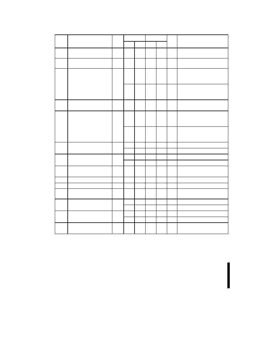
28F004S3/28F008S3/28F016S3
E
30
PRELIMINARY
6.4
DC Characteristics--Commercial Temperature
2.7 V V
CC
3.3 V V
CC
Test
Sym
Parameter
Notes Typ
Max
Typ
Max
Unit
Conditions
I
LI
Input Load Current
1
±
0.5
±
0.5
µ
A
V
CC
= V
CC
Max
V
IN
= V
CC
or GND
I
LO
Output Leakage Current
1
±
0.5
±
0.5
µ
A
V
CC
= V
CC
Max
V
OUT
= V
CC
or GND
I
CCS
V
CC
Standby Current
1,3,6
20
100
20
100
µ
A
CMOS Inputs
V
CC
= V
CC
Max
CE# = RP# = V
CC
± 0.2 V
0.1
2
0.2
2
mA
TTL Inputs
V
CC
= V
CC
Max
CE# = RP# = V
IH
I
CCD
V
CC
Deep Power-Down
Current
1
10
10
µ
A
RP# = GND ± 0.2 V
I
OUT
(RY/BY#) = 0 mA
I
CCR
V
CC
Read Current
1,5,6
6
15
7
15
mA
CMOS Inputs
V
CC
= V
CC
Max, CE# = GND
f = 5 MHz, I
OUT
= 0 mA
7
18
8
18
mA
TTL Inputs
V
CC
= V
CC
Max, CE# = GND
f = 5 MHz, I
OUT
= 0 mA
I
CCW
V
CC
Program/ Set
1,7
17
mA
V
PP
= 3.3 V ± 0.3 V
Lock-Bit Current
12
mA
V
PP
= 12.0 V ± 5%
I
CCE
V
CC
Block Erase/Clear
1,7
17
mA
V
PP
= 3.3 V ± 0.3 V
Block Lock-Bits Current
12
mA
V
PP
= 12.0 V ± 5%
I
CCWS
I
CCES
V
CC
Program/Block
Erase Suspend Current
1,2
6
mA
CE# = V
IH
I
PPS
V
PP
Standby Current
1
± 2
± 15
± 2
± 15
µA
V
PP
V
CC
I
PPR
V
PP
Read Current
1
10
200
10
200
µA
V
PP
> V
CC
I
PPD
V
PP
Deep Power-Down
Current
1
0.1
5
0.1
5
µA
RP# = GND ± 0.2 V
I
PPW
V
PP
Program/Set
1,7
40
mA
V
PP
= 3.3 V ± 0.3 V
Lock-Bit Current
15
mA
V
PP
= 12.0 V ± 5%
I
PPE
V
PP
Block Erase/Clear
1,7
20
mA
V
PP
= 3.3 V ± 0.3 V
Block Lock-Bits Current
15
mA
V
PP
= 12.0 V ± 5%
I
PPWS
I
PPES
V
PP
Block Erase/Program
Suspend Current
1
10
200
µA
V
PP
= V
PPH1/2

E
28F004S3/28F008S3/28F016S3
31
PRELIMINARY
6.4
DC Characteristics-- Commercial Temperature
(Continued)
2.7 V V
CC
3.3 V V
CC
Test
Sym
Parameter
Notes Min
Max
Min
Max Unit
Conditions
V
IL
Input Low Voltage
7
≠0.5
0.8
≠0.5
0.8
V
V
IH
Input High Voltage
7
2.0
V
CC
+ 0.5
2.0
V
CC
+ 0.5
V
V
OL
Output Low Voltage
3,7
0.4
0.4
V
V
CC
= V
CC
Min
I
OL
= 2 mA
V
OH1
Output High Voltage
(TTL)
3,7
2.4
2.4
V
V
CC
= V
CC
Min
I
OH
= ≠2.5 mA
V
OH2
Output High Voltage
(CMOS)
3,7
0.85
V
CC
0.85
V
CC
V
V
CC
= V
CC
Min
I
OH
= ≠2.5 mA
V
CC
≠0.4
V
CC
≠0.4
V
V
CC
= V
CC
Min
I
OH
= ≠100 µA
V
PPLK
V
PP
Lockout Voltage
4,7
1.5
1.5
V
V
PPH1
V
PP
Voltage
2.7
3.6
2.7
3.6
V
V
PPH2
V
PP
Voltage
11.4
12.6
V
V
LKO
V
CC
Lockout Voltage
2.0
2.0
V
V
HH
RP# Unlock Voltage
8,9
11.4
12.6
V
Set Master Lock-Bit
Override Lock-Bit
NOTES:
1. All currents are in RMS unless otherwise noted. Typical values at nominal V
CC
voltage and T
A
= +25
∞
C. These currents are
valid for all product versions (packages and speeds).
2. I
CCWS
and I
CCES
are specified with the device de-selected. If read or written while in erase suspend mode, the device's
current is the sum of I
CCWS
or I
CCES
and I
CCR
or I
CCW
.
3. Includes RY/BY#.
4. Block erases, program, and lock-bit configurations are inhibited when V
PP
V
PPLK
, and not guaranteed in the range
between V
PPLK
(max) and V
PPH1
(min), between V
PPH1
(max) and V
PPH2
(min), and above V
PPH2
(max).
5. Automatic Power Savings (APS) reduces typical I
CCR
to 3 mA at 3.3 V V
CC
in static operation.
6. CMOS inputs are either V
CC
± 0.2 V or GND ± 0.2 V. TTL inputs are either V
IL
or V
IH
.
7. Sampled, not 100% tested.
8. Master lock-bit set operations are inhibited when RP# = V
IH
. Block lock-bit configuration operations are inhibited when the
master lock-bit is set and RP# = V
IH
. Block erases and program are inhibited when the corresponding block-lock bit is set
and RP# = V
IH
. Block erase, program, and lock-bit configuration operations are not guaranteed and should not be
attempted with V
IH
< RP# < V
HH
.
9. RP# connection to a V
HH
supply is allowed for a maximum cumulative period of 80 hours.
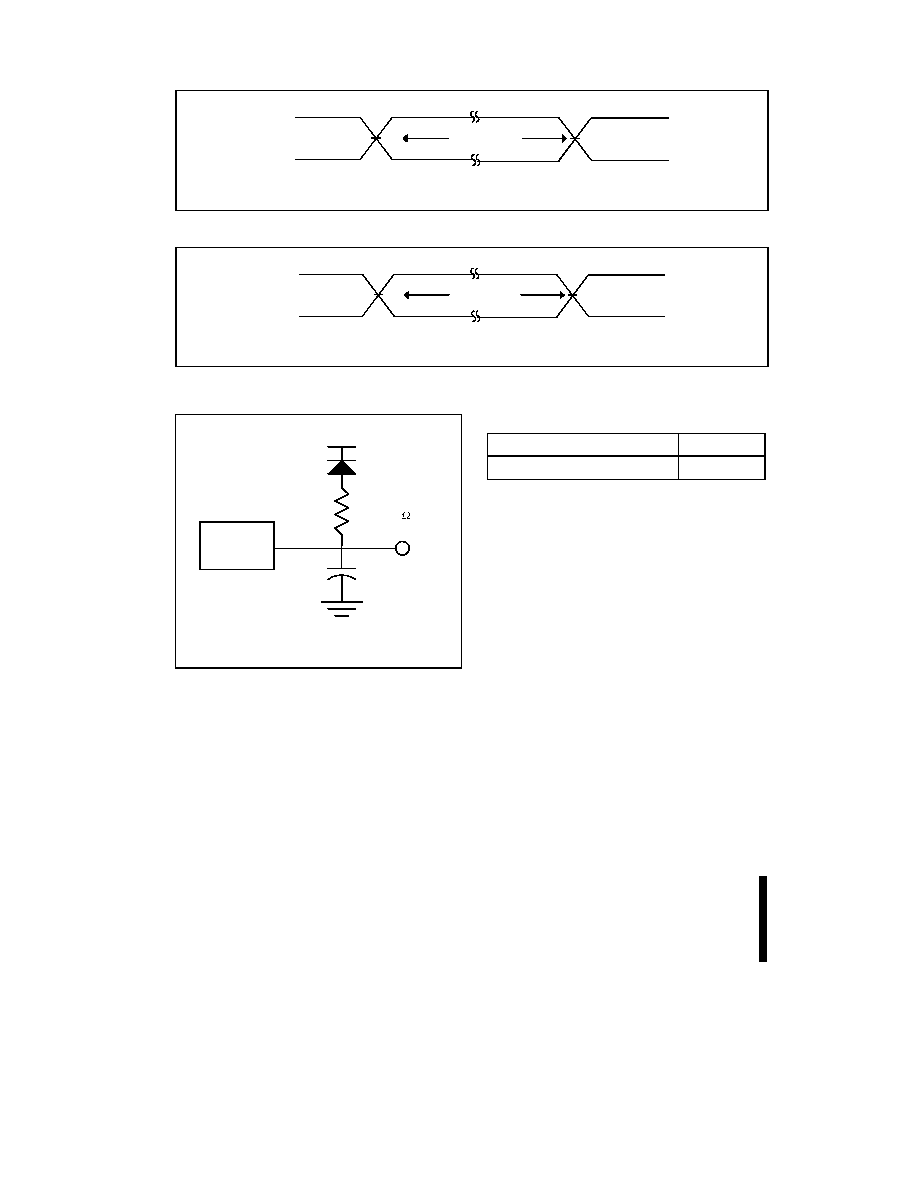
28F004S3/28F008S3/28F016S3
E
32
PRELIMINARY
TEST POINTS
INPUT
OUTPUT
1.35
2.7
0.0
1.35
AC test inputs are driven at 2.7 V for a Logic "1" and 0.0 V for a Logic "0." Input timing begins, and output timing ends, at
1.35 V. Input rise and fall times (10% to 90%) <10 ns.
Figure 13. Transient Input/Output Reference Waveform for V
CC
= 2.7 V
-
3.6 V
TEST POINTS
INPUT
OUTPUT
1.5
3.0
0.0
1.5
AC test inputs are driven at 3.0 V for a Logic "1" and 0.0 V for a Logic "0." Input timing begins, and output timing ends, at 1.5 V.
Input rise and fall times (10% to 90%) <10 ns.
Figure 14. Transient Input/Output Reference Waveform for V
CC
= 3.3 V ± 0.3 V
DEVICE
UNDER
TEST
1.3V
1N914
R
L
C
L
OUT
= 3.3 K
NOTE:
C
L
includes Jig Capacitance
Figure 15. Transient Equivalent Testing
Load Circuit
Test Configuration Capacitance Loading Value
Test Configuration
C
L
(pF)
V
CC
= 3.3 V
±
0.3 V, 2.7 V
-
3.6 V
50

E
28F004S3/28F008S3/28F016S3
33
PRELIMINARY
IH
V
IL
V
RP# (P)
IH
V
IL
V
RY/BY# (R)
P1
P2
Figure 16. AC Waveform for Reset Operation
Table 7. Reset Specifications
(1)
--Commercial Temperature
2.7 V V
CC
3.3 V V
CC
#
Sym
Parameter
Notes Min
Max
Min
Max
Unit
P1
t
PLPH
RP# Pulse Low Time (If RP# is tied to V
CC
, this
specification is not applicable)
100
100
ns
P2
t
PLRH
RP# Low to Reset during Block Erase, Program, or
Lock-Bit Configuration
2,3
20
µs
NOTES:
1.
These specifications are valid for all product versions (packages and speeds).
2.
If RP# is asserted when the WSM is not busy (RY/BY# = "1"), the reset will complete within 100 ns.
3.
A reset time, t
PHQV
, is required from the latter of RY/BY# or RP# going high until outputs are valid.
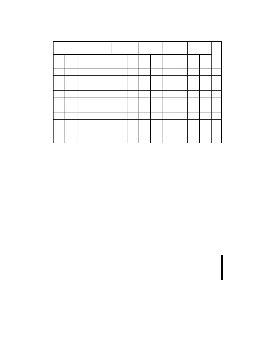
28F004S3/28F008S3/28F016S3
E
34
PRELIMINARY
6.5
AC Characteristics--Read-Only Operations
(1, 4)
--
Commercial Temperature
T
A
= 0 ∞C to +70 ∞C
3.3V ± 0.3V V
CC
≠120
≠150
Versions
(4)
2.7V
-
3.6V V
CC
≠150
≠170
Unit
#
Sym
Parameter
Notes
Min
Max
Min
Max
Min
Max
R1
t
AVAV
Read Cycle Time
120
150
170
ns
R2
t
AVQV
Address to Output Delay
120
150
170
ns
R3
t
ELQV
CE# to Output Delay
2
120
150
170
ns
R4
t
GLQV
OE# to Output Delay
2
50
55
55
ns
R5
t
PHQV
RP# High to Output Delay
600
600
600
ns
R6
t
ELQX
CE# to Output in Low Z
3
0
0
0
ns
R7
t
GLQX
OE# to Output in Low Z
3
0
0
0
ns
R8
t
EHQZ
CE# High to Output in High Z
3
55
55
55
ns
R9
t
GHQZ
OE# High to Output in High Z
3
20
20
25
ns
R10
t
OH
Output Hold from Address,
CE# or OE# Change,
Whichever Occurs First
3
0
0
0
ns
NOTES:
1.
See AC Input/Output Reference Waveform for maximum allowable input slew rate.
2.
OE# may be delayed up to t
ELQV
≠t
GLQV
after the falling edge of CE# without impact on t
ELQV
.
3.
Sampled, not 100% tested.
4.
See
Ordering Information for device speeds (valid operational combinations).
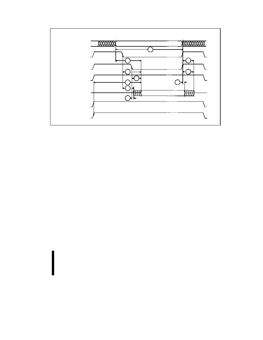
E
28F004S3/28F008S3/28F016S3
35
PRELIMINARY
V
CC
Address Stable
Device
Address Selection
IH
V
IL
V
ADDRESSES (A)
IH
V
IL
V
IH
V
IL
V
CE# (E)
OE# (G)
Data
Valid
Standby
IH
V
IL
V
WE# (W)
DATA (D/Q)
(DQ0-DQ7)
OL
V
OH
V
High Z
Valid Output
High Z
IH
V
IL
V
RP# (P)
R1
R3
R4
R7
R6
R2
R5
R8
R9
R10
Figure 17. AC Waveform for Read Operations
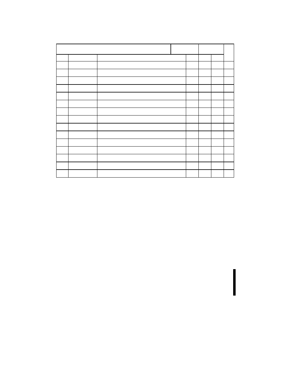
28F004S3/28F008S3/28F016S3
E
36
PRELIMINARY
6.6
AC Characteristics--Write Operations
(1, 2)
--Commercial Temperature
T
A
= 0 ∞C to +70 ∞C
Versions
(4)
3.3V ± 0.3V,
2.7V
-
3.6V V
CC
Valid for All
Speeds
Unit
#
Sym
Parameter
Notes
Min
Max
W1
t
PHWL
(t
PHEL
)
RP# High Recovery to WE# (CE#) Going Low
3
1
µs
W2
t
ELWL
(t
WLEL
)
CE# (WE#) Setup to WE# (CE#) Going Low
7
0
ns
W3
t
WP
Write Pulse Width
7
70
ns
W4
t
DVWH
(t
DVEH
)
Data Setup to WE# (CE#) Going High
4
50
ns
W5
t
AVWH
(t
AVEH
)
Address Setup to WE# (CE#) Going High
4
50
ns
W6
t
WHEH
(t
EHWH
)
CE# (WE#) Hold from WE# (CE#) High
0
ns
W7
t
WHDX
(t
EHDX
)
Data Hold from WE# (CE#) High
5
ns
W8
t
WHAX
(t
EHAX
)
Address Hold from WE# (CE#) High
5
ns
W9
t
WPH
Write Pulse Width High
9
25
ns
W10
t
PHHWH
(t
PHHEH
) RP# V
HH
Setup to WE# (CE#) Going High
3,8
100
ns
W11
t
VPWH
(t
VPEH
)
V
PP
Setup to WE# (CE#) Going High
3,8
100
ns
W12
t
WHRL
(t
EHRL
)
WE# (CE#) High to RY/BY# Going Low
8
90
ns
W13
t
WHGL
(t
EHGL
)
Write Recovery before Read
0
ns
W14
t
QVPH
RP# V
HH
Hold from Valid SRD, RY/BY# High
3,5,8
0
ns
W15
t
QVVL
V
PP
Hold from Valid SRD, RY/BY# High
3,5,8
0
ns
NOTES:
1.
Read timing characteristics during block erase, program, and lock-bit configuration operations are the same as during
read-only operations. Refer to
AC Characteristics--Read-Only Operations.
2.
A write operation can be initiated and terminated with either CE# or WE#.
3.
Sampled, not 100% tested.
4.
Refer to Table 3 for valid A
IN
and D
IN
for block erase, program, or lock-bit configuration.
5.
V
PP
should be held at V
PPH1/2
(and if necessary RP# should be held at V
HH
) until determination of block erase, program, or
lock-bit configuration success (SR.1/3/4/5 = 0).
6.
See Ordering Information for device speeds (valid operational combinations).
7.
Write pulse width (t
WP
) is defined from CE# or WE# going low (whichever goes low last) to CE# or WE# going high
(whichever goes high first). Hence, t
WP
= t
WLWH
= t
ELEH
= t
WLEH
= t
ELWH
. If CE# is driven low 10 ns before WE# going low,
WE# pulse width requirement decreases to t
WP
- 20 ns.
8. Block erase, program, and lock-bit configuration with V
CC
<
2.7 V should not be attempted.
9.
Write pulse width high (t
WPH
) is defined from CE# or WE# going high (whichever goes high first) to CE# or WE# going low
(whichever goes low last). Hence, t
WPH
= t
WHWL
= t
EHEL
= t
WHEL
= t
EHWL
.
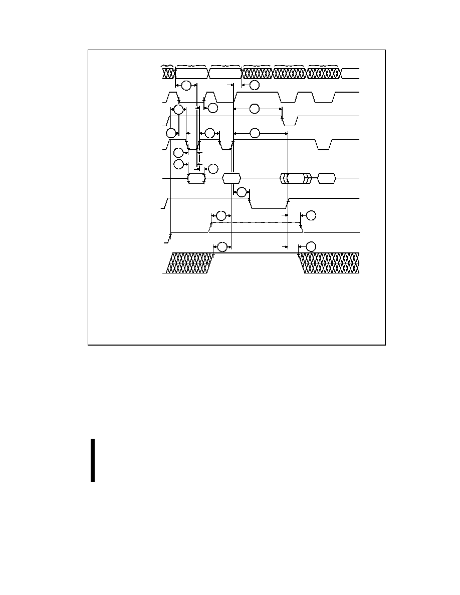
E
28F004S3/28F008S3/28F016S3
37
PRELIMINARY
W3
ADDRESSES [A]
DATA [D/Q]
IH
V
IL
V
IH
V
IL
V
IH
V
IL
V
IH
V
IL
V
IL
V
IN
D
IN
A
IN
A
Valid
SRD
IN
D
High Z
IH
V
IL
V
V [V]
PP
A
B
C
D
F
E
PPH2,1
V
PPLK
V
IN
D
RP# [P]
HH
V
IL
V
IH
V
RY/BY# [R]
IH
V
IL
V
CE# (WE#) [E(W)]
WE# (CE#) [W(E)]
OE# [G]
W1
W2
W4
W5
W6
W9
W7
W16
W12
W8
W13
W10
W15
W14
W11
NOTES:
A.
V
CC
power-up and standby.
B.
Write block erase or program setup.
C.
Write block erase confirm or valid address and data..
D.
Automated erase or program delay.
E.
Read status register data.
F.
Write Read Array command.
Figure 18. AC Waveform for Write Operations

28F004S3/28F008S3/28F016S3
E
38
PRELIMINARY
6.7
Block Erase, Program, and Lock-Bit Configuration Performance
(3, 4, 5)
--
Commercial Temperature
V
CC
= 3.3V ± 0.3V, T
A
= 0 ∞C to +70 ∞C
2.7 V V
PP
3.3 V V
PP
12 V V
PP
#
Sym
Parameter
Notes Typ
(1)
Max
Typ
(1)
Max
Typ
(1)
Max
Unit
W16
t
WHRH1
t
EHRH1
Byte Program Time
2
TBD
TBD
17
300
7.0
125
µs
Block Program Time
2
TBD
TBD
1.1
4.0
0.5
1.5
sec
W16
t
WHRH2
t
EHRH2
Block Erase Time
2
TBD
TBD
0.8
6.0
0.3
4.0
sec
W16
t
WHRH3
t
EHRH3
Set Lock-Bit Time
2
TBD
TBD
21
TBD
11.6
TBD
µs
W16
t
WHRH4
t
EHRH4
Clear Block Lock-Bits Time
2
TBD
TBD
1.8
TBD
1.1
TBD
sec
W16
t
WHRH5
t
EHRH5
Program Suspend Latency
Time
TBD
TBD
7.1
10
7.4
10.4
µs
W16
t
WHRH6
t
EHRH6
Block Erase Suspend
Latency Time
TBD
TBD
15.2
21.1
12.3
17.2
µs
NOTES:
1.
Typical values measured at T
A
= +25 ∞C and nominal voltages. Assumes corresponding lock-bits are not set. Subject to
change based on device characterization.
2.
Excludes system-level overhead.
3.
These performance numbers are valid for all speed versions.
4.
Sampled, but not 100% tested.
5. Reference
the
AC Waveform for Write Operations, Figure 18.

E
28F004S3/28F008S3/28F016S3
39
PRELIMINARY
6.8
Extended Temperature Operating Conditions
Except for the specifications given in this section, all DC and AC characteristics are identical to those give in
commercial temperature specifications. See the Section 6.2 for commercial temperature specifications.
Extended Temperature and V
CC
Operating Conditions
Symbol
Parameter
Notes
Min
Max
Unit
Test Condition
T
A
Operating Temperature
≠40
+85
∞C
Ambient Temperature
6.9
DC Characteristics--Extended Temperature
T
A
= ≠40 ∞C to +85 ∞C
2.7 V V
CC
3.3 V V
CC
Test
Sym
Parameter
Notes Typ
Max
Typ
Max
Unit
Conditions
I
CCD
V
CC
Deep Power-Down
Current
1
20
20
µ
A
RP# = GND ± 0.2 V
I
OUT
(RY/BY#) = 0 mA
NOTE:
1.
All currents are in RMS unless otherwise noted. These currents are valid for all product versions (packages and speeds).
Contact Intel's Application Support Hotline or your local sales office for information about typical specifications.
6.10
AC Characteristics--Read-Only Operations
(1, 3)
--Extended Temperature
T
A
= ≠40 ∞C to +85 ∞C
3.3 V ± 0.3 V V
CC
≠150
Versions
(3)
2.7 V
-
3.6 V V
CC
≠170
Unit
#
Sym
Parameter
Notes
Min
Max
Min
Max
R1
t
AVAV
Read Cycle Time
150
170
ns
R2
t
AVQV
Address to Output Delay
150
170
ns
R3
t
ELQV
CE# to Output Delay
2
150
170
ns
NOTES:
1.
See AC Input/Output Reference Waveform for maximum allowable input slew rate.
2.
OE# may be delayed up to t
ELQV≠
t
GLQV
after the falling edge of CE# without impact on t
ELQV
.
3.
See
Ordering Information for device speeds (valid operational combinations).

28F004S3/28F008S3/28F016S3
E
40
PRELIMINARY
7.0
ORDERING INFORMATION
E 2 8 F 0 0 4 S 3 - 1 2
Operating Temperature/Package
E = Comm. Temp. 40-Lead TSOP
TE = Extended Temp. 40-Lead TSOP
PA = Comm. Temp 44-Lead PSOP
TB = Ext. Temp 44-Lead PSOP
G = Comm. Temp. 40-Ball µBGA* CSP
Product line designator for all Intel Flash products
Access Speed (ns)
120 ns (3.3 V), 150 ns (2.7 V)
Product Family
S = FlashFileTM Memory
Device Density
004 = 4 Mbit
008 = 8 Mbit
016 = 16 Mbit
Voltage Options (V
CC
/V
PP
)
3 = Smart 3 Flash
(2.7 V/ 2.7 V and 3.3 V/3.3 V and 12 V)
0
Order Code by Density
(1)
Valid Operational Combinations
4 Mbit
8 Mbit
16 Mbit
2.7V≠3.6V V
CC
50 pF load
3.3V
±
0.3V V
CC
50 pF load
Commercial Temperature
E28F004S3-120
E28F008S3-120
E28F016S3-120
≠150
≠120
E28F004S3-150
E28F008S3-150
E28F016S3-150
≠170
≠150
PA28F004S3-120
PA28F008S3-120
PA28F016S3-120
≠150
≠120
PA28F004S3-150
PA28F008S3-150
PA28F016S3-150
≠170
≠150
G28F008S3-120
G28F016S3-120
≠150
≠120
G28F008S3-150
G28F016S3-150
≠170
≠150
Extended Temperature
TE28F004S3-150
TE28F008S3-150
TE28F016S3-150
≠170
≠150
TB28F004S3-150
TB28F008S3-150
TB28F016S3-150
≠170
≠150
NOTE:
1.
Contact your local Intel or distribution sales office to order components with 2.7 V V
PP
capability.

E
28F004S3/28F008S3/28F016S3
41
PRELIMINARY
8.0
ADDITIONAL INFORMATION
Order Number
Document/Tool
290597
5 Volt FlashFileTM Memory; 28F004S5, 28F008S5, 28F016S5 datasheet
292182
AP-627 Byte-Wide FlashFileTM Memory Family Software Drivers
292123
AP-374 Flash Memory Write Protection Techniques
297799
3 Volt FlashFileTM Memory; 28F004S3, 28F008S3, 28F016S3 Specification
Update
Note 3
AP-625 28F008SC Compatibility with 28F008SA
Note 3
AP-364 28F008SA Automation and Algorithms
Note 3
AP-359 28F008SA Hardware Interfacing
Note 3
AB-64 4-, 8-, 16-Mbit Byte-Wide FlashFileTM Memory Family Overview
Contact Intel/Distribution
Sales Office
4-, 8-, and 16-Mbit Schematic Symbols
Contact Intel/Distribution
Sales Office
4-, 8-, and 16-Mbit TimingDesigner* Files
Contact Intel/Distribution
Sales Office
4-, 8-, and 16-Mbit VHDL and Verilog Models
Contact Intel/Distribution
Sales Office
4-, 8-, and 16-Mbit iBIS Models
NOTES:
1.
Please call the Intel Literature Center at (800) 548-4725 to request Intel documentation. International customers should
contact their local Intel or distribution sales office.
2.
Visit Intel's World Wide Web home page at http://www.intel.com for technical documentation and tools.
3.
These documents can be located at the Intel World Wide Web support site, http://www.intel.com/support/flash/memory