 | –≠–ª–µ–∫—Ç—Ä–æ–Ω–Ω—ã–π –∫–æ–º–ø–æ–Ω–µ–Ω—Ç: 28F640K3 | –°–∫–∞—á–∞—Ç—å:  PDF PDF  ZIP ZIP |

Intel StrataFlash
Æ
Synchronous Memory
(K3/K18)
28F640K3, 28F640K18, 28F128K3, 28F128K18, 28F256K3,
28F256K18 (x16)
Datasheet
Product Features
The Intel StrataFlash
Æ
Synchronous Memory (K3/K18) product line adds a high performance
burst-mode interface and other additional features to the Intel StrataFlash
Æ
memory family of
products. Just like its J3 counterpart, the K3/K18 device utilizes reliable and proven two-bit-per-
cell technology to deliver 2x the memory in 1x the space, offering high density flash at low cost.
This is Intel's third generation MLC technology, manufactured on 0.18 µm lithography, making
it the most widely used and proven MLC product family on the market.
K3/K18 is a 3-volt device (core), but it is available with 3-volt (K3) or 1.8-volt (K18) I/O
voltages. These devices are ideal for mainstream applications requiring large storage space for
both code and data storage. Advanced system designs will benefit from the high performance
page and burst modes for direct execution from the flash memory. Available in densities from 64
Mbit to 256 Mbit (32 Mbyte), the K3/K18 device is the highest density NOR-based flash
component available today, just as it was when Intel introduced the original device in 1997.
Performance
--110/115/120 ns Initial Access Speed for
64/128/256 Mbit Densities
--25 ns Asynchronous Page-Mode Reads,
8 Words Wide
--13 ns Synchronous Burst-Mode Reads,
8 or 16 Words Wide
--32-Word Write Buffer
--Buffered Enhanced Factory
Programming
Software
--25 µs (typ.) Program and Erase Suspend
Latency Time
--Flash Data Integrator (FDI), Common
Flash Interface (CFI) Compatible
--Programmable WAIT Signal Polarity
Quality and Reliability
--Operating Temperature:
≠40 ∞C to +85 ∞C
--100K Minimum Erase Cycles per Block
--0.18 µm ETOXTM VII Process
Architecture
--Multi-Level Cell Technology: High
Density at Low Cost
--Symmetrical 64 K-Word Blocks
--256 Mbit (256 Blocks)
--128 Mbit (128 Blocks)
--64 Mbit (64 Blocks)
--Ideal for "CODE + DATA" applications
Security
--2-Kbit Protection Register
--Unique 64-bit Device Identifier
--Absolute Data Protection with V
PEN
and
WP#
--Individual and Instantaneous Block
Locking, Unlocking and Lock-Down
Capability
Packaging and Voltage
--64-Ball Intel
Æ
Easy BGA Package
--56-and 79-Ball Intel
Æ
VF BGA Package
--V
CC
= 2.70 V ≠ 3.60 V
--V
CCQ
= 1.65 ≠ 1.95 V or 2.375≠ 3.60 V
Order Number: 290737-006
June 2003
Notice: This document contains information on new products in production. The specifications
are subject to change without notice. Verify with your local Intel sales office that you have the lat-
est datasheet before finalizing a design.

2
Datasheet
Information in this document is provided in connection with Intel
Æ
products. No license, express or implied, by estoppel or otherwise, to any intellectual
property rights is granted by this document. Except as provided in Intel's Terms and Conditions of Sale for such products, Intel assumes no liability
whatsoever, and Intel disclaims any express or implied warranty, relating to sale and/or use of Intel products including liability or warranties relating to
fitness for a particular purpose, merchantability, or infringement of any patent, copyright or other intellectual property right. Intel products are not
intended for use in medical, life saving, or life sustaining applications.
Intel may make changes to specifications and product descriptions at any time, without notice.
Designers must not rely on the absence or characteristics of any features or instructions marked "reserved" or "undefined." Intel reserves these for
future definition and shall have no responsibility whatsoever for conflicts or incompatibilities arising from future changes to them.
The 3 Volt Synchronous Intel StrataFlash
Æ
Memory may contain design defects or errors known as errata which may cause the product to deviate
from published specifications. Current characterized errata are available on request.
Contact your local Intel sales office or your distributor to obtain the latest specifications and before placing your product order.
Copies of documents which have an ordering number and are referenced in this document, or other Intel literature may be obtained by calling 1-800-
548-4725 or by visiting Intel's website at http://www.intel.com.
Copyright © Intel Corporation, 2003.
*Other names and brands may be claimed as the property of others.

Datasheet
3
28F640K3, 28F640K18, 28F128K3, 28F128K18, 28F256K3, 28F256K18
Contents
1.0
Introduction
..................................................................................................................7
1.1
Document Purpose................................................................................................7
1.2
Nomenclature ........................................................................................................7
1.3
Conventions ..........................................................................................................8
2.0
Device Description
....................................................................................................9
2.1
Product Overview ..................................................................................................9
2.1.1
High Performance Page/Burst Modes......................................................9
2.1.2
Single Chip Solution .................................................................................9
2.1.3
Packaging Options .................................................................................10
2.1.4
Product Highlights ..................................................................................10
2.2
Package Diagram................................................................................................11
2.3
Signal Descriptions..............................................................................................14
2.4
Block Diagram .....................................................................................................15
2.5
Memory Map .......................................................................................................16
3.0
Device Operations
...................................................................................................17
3.1
Bus Operations....................................................................................................17
3.1.1
Read Mode.............................................................................................17
3.1.2
Write/Program ........................................................................................18
3.1.3
Output Disable........................................................................................18
3.1.4
Standby ..................................................................................................18
3.1.5
Reset ......................................................................................................18
3.2
Device Commands ..............................................................................................19
4.0
Read Modes
................................................................................................................21
4.1
Asynchronous Page-Mode Read ........................................................................21
4.2
Synchronous Burst-Mode Read ..........................................................................22
4.3
Read Configuration Register ...............................................................................22
4.3.1
Read Mode.............................................................................................23
4.3.2
Latency Count ........................................................................................23
4.3.3
WAIT Polarity .........................................................................................25
4.3.4
Data Hold ...............................................................................................25
4.3.5
WAIT Delay ............................................................................................26
4.3.6
Burst Sequence......................................................................................26
4.3.7
Clock Edge .............................................................................................26
4.3.8
Burst Length ...........................................................................................26
5.0
Program Modes
.........................................................................................................27
5.1
Word Programming .............................................................................................27
5.2
Write-Buffer Programming...................................................................................27
5.3
Program Suspend ...............................................................................................28
5.4
Program Resume ................................................................................................29
5.5
Buffered Enhanced Factory Programming (Buffered-EFP).................................29
5.5.1
Buffered-EFP Requirements and Considerations ..................................29
5.5.2
Buffered-EFP Setup Phase ....................................................................30
5.5.3
Buffered-EFP Program and Verify Phase ..............................................30

28F640K3, 28F640K18, 28F128K3, 28F128K18, 28F256K3, 28F256K18
4
Datasheet
5.5.4
Buffered-EFP Exit Phase ....................................................................... 31
6.0
Erase Mode
................................................................................................................. 32
6.1
Block Erase ......................................................................................................... 32
6.2
Erase Suspend.................................................................................................... 32
6.3
Erase Resume .................................................................................................... 33
7.0
Security Modes
......................................................................................................... 34
7.1
Block Locking Operations ................................................................................... 34
7.1.1
Block Lock.............................................................................................. 35
7.1.2
Block Unlock .......................................................................................... 35
7.1.3
Block Lock-Down ................................................................................... 35
7.1.4
Block Lock During Erase Suspend......................................................... 35
7.1.5
WP# Lock-Down Control........................................................................ 35
7.2
Protection Registers............................................................................................ 36
7.2.1
Reading the Protection Registers .......................................................... 37
7.2.2
Programming the Protection Registers .................................................. 37
7.2.3
Locking the Protection Registers ........................................................... 37
7.3
Array Protection .................................................................................................. 37
8.0
Special Modes
........................................................................................................... 38
8.1
Read Status Register .......................................................................................... 38
8.1.1
Clear Status Register ............................................................................. 39
8.2
Read Device Identifier......................................................................................... 39
8.3
Read Query/CFI .................................................................................................. 40
8.4
STS Configuration (Easy BGA package ONLY) ................................................. 40
9.0
Power and Reset
...................................................................................................... 41
9.1
Power-Up/Down Characteristics ......................................................................... 41
9.2
Power Supply Decoupling ................................................................................... 41
9.3
Reset Characteristics .......................................................................................... 41
10.0
Electrical Specifications
........................................................................................ 42
10.1
Absolute Maximum Ratings ................................................................................ 42
10.2
Operating Conditions .......................................................................................... 42
10.3
DC Current Characteristics ................................................................................. 43
10.4
Read Operations ................................................................................................. 45
10.5
Write Operation ................................................................................................... 50
10.6
Block Erase and Program Operation Performance ............................................. 52
10.7
Reset Operation .................................................................................................. 53
10.8
AC Test Conditions ............................................................................................. 54
10.9
Capacitance ........................................................................................................ 54
Appendix A Write State Machine (WSM)
...............................................................................55
Appendix B Common Flash Interface
....................................................................................60
Appendix C Flowcharts
...............................................................................................................66
Appendix D Mechanical Package Information
...................................................................74
Appendix E Additional Information
........................................................................................77
Appendix F Order Information
..................................................................................................78

Datasheet
5
28F640K3, 28F640K18, 28F128K3, 28F128K18, 28F256K3, 28F256K18
Revision History
Date of
Revision
Revision
Description
08/22/01
-001
Original Version
09/24/01
-002
Corrected Typographical Errors in 11.0 AC Characteristics section.
09/27/01
-003
Change VFBGA Package from 64 to 56 ball package. Add ordering info in
Appendix E.
02/22/02
-004
Changes to ballouts per engineering review and editing/formatting updates.
06/17/02
-005
Changes to Iccr, elimination of Speed Bin 2, expansion of Vccq range.
06/11/03
-006
Corrections to Ordering Information, typcs, added Next-State Table, Appendix A
info. Added table of Latency Count settings to Section 4.3.2.

28F640K3, 28F640K18, 28F128K3, 28F128K18, 28F256K3, 28F256K18
6
Datasheet

28F640K3, 28F640K18, 28F128K3, 28F128K18, 28F256K3, 28F256K18
Datasheet
7
1.0
Introduction
1.1
Document Purpose
This document contains information pertaining to the Intel StrataFlash
Æ
Synchronous Memory
(K3/K18) device. The purpose of this document is to describe the features, operations and
specifications of these devices.
1.2
Nomenclature
3 Volt core:
V
CC
range of 2.7 V ≠ 3.6 V
3 Volt I/O:
V
CCQ
range of 2.375 V ≠ 3.6 V
1.8 Volt I/O:
V
CCQ
range of 1.65 V ≠ 1.95 V
A
MIN
:
For Easy BGA packages: A
MIN
= A1
For VF BGA packages: A
MIN
= A0
A
MAX
:
For Easy BGA packages:
64 Mbit A
MAX
= A22
128 Mbit A
MAX
= A23
256 Mbit A
MAX
= A24
For VF BGA packages:
64 Mbit A
MAX
= A21
128 Mbit A
MAX
= A22
256 Mbit A
MAX
= A23
Block:
A group of flash cells that share common erase circuitry and erase simultaneously
Program:
To write data to the flash array
VPEN:
Refers to a signal or package connection name
V
PEN
:
Refers to timing or voltage levels
CUI:
Command User Interface
OTP:
One Time Programmable
PR:
Protection Register
PLR:
Protection Lock Register
RFU:
Reserved for Future Use
SR:
Status Register
RCR:
Read Configuration Register
WSM:
Write State Machine
MLC:
Multi-Level Cell
Set:
Indicates a logic one (1)
Clear:
Indicates a logic zero (0)

28F640K3, 28F640K18, 28F128K3, 28F128K18, 28F256K3, 28F256K18
8
Datasheet
1.3
Conventions
0x:
Hexadecimal prefix
0b:
Binary prefix
k (noun):
1,000
M (noun):
1,000,000
Byte:
8 bits
Word:
16 bits
Kword:
1,024 words
Kb:
1,024 bits
KB:
1,024 bytes
Mb:
1,048,576 bits
MB:
1,048,576 bytes
Brackets:
Square brackets ([]) will be used to designate group membership or to define a
group of signals with similar function (i.e. A[21:1], SR[4,1] and D[15:0]).

28F640K3, 28F640K18, 28F128K3, 28F128K18, 28F256K3, 28F256K18
Datasheet
9
2.0
Device Description
This section provides an overview of the K3/K18 device features, packaging information, signal
names, and device architecture.
2.1
Product Overview
The K3/K18 device product line adds a high performance burst-mode interface and other
additional features to the Intel StrataFlash
Æ
memory family of products. Just like its J3 counterpart,
the K3/K18 utilizes reliable and proven two-bit-per-cell technology to deliver 2x the memory in 1x
the space, offering high density flash at low cost. This is the third generation of Intel's multi-level
cell (MLC) technology, manufactured on 0.18 µm lithography, making it the most widely used and
proven MLC product family on the market.
K3/K18 is a 3-volt device (core), but it is available with 3-volt (K3) or 1.8-volt (K18) I/O voltages.
These devices are ideal for mainstream applications requiring large storage space for both code and
data storage. Advanced system designs will benefit from the high performance page and burst
modes for direct execution from the flash memory. Available in densities from 64 Mb to 256 Mbit
(32 Mbyte), the K3/K18 device is the highest density NOR-based flash component available today,
just as it was when Intel introduced the original device in 1997.
2.1.1
High Performance Page/Burst Modes
NOR-based flash is generally preferred over other architectures for its reliability and fast read
speeds. Fast reads allow the application to execute code directly out of flash, rather than
downloading to RAM for execution, saving the costs of redundant system memory and board
space. The K3/K18 device sets the standard for fast read speeds by adding burst mode and utilizing
an 8 word page mode. Burst mode increases throughput up to 76MB/s, effectively five times faster
than asynchronous reads on standard flash memory, and supports performance up to 66 Mhz with
zero wait states. Both page and burst modes also provide a high performance glueless interface to
the Intel
Æ
StrongARM* SA-1110 CPU (and future Intel
Æ
XScale processors) and many other
microprocessors.
2.1.2
Single Chip Solution
In addition to code execution, many applications also have data storage needs. K3/K18 memory
provides a single-chip solution for combined code execution and data storage. A single-chip
solution is easy to implement by utilizing a unique hardware and software combination: the K3/
K18 device and Intel
Æ
Persistent Storage Manager (Intel
Æ
PSM). Intel
Æ
PSM is royalty free when
used with Intel
Æ
Flash, is an installable file system and block device driver for Microsoft
Windows* CE OS version 2.1 and later.
The Intel
Æ
PSM software is appropriate for any application using the Microsoft Windows CE
operating system, including PC Companions, Set-Top Boxes, and other connected appliances and
hand-held devices. Other operating system ports are also available. Intel
Æ
PSM is optimized for the
Intel StrataFlash
Æ
Memory product line.
For wireless applications, Intel
Æ
Flash Data Integrator (Intel
Æ
FDI) Version 4 software provides the
ability to manage data and files in Intel StrataFlash
Æ
Memory in an open architecture, including
support for downloaded Java* applets, Bluetooth* file transfers, and voice recognition tags.

28F640K3, 28F640K18, 28F128K3, 28F128K18, 28F256K3, 28F256K18
10
Datasheet
2.1.3
Packaging Options
The K3/K18 device is available in multiple packages: Easy BGA and VF BGA, and Stacked Chip
Scale Package (SCSP, stacking with SRAM or flash + flash). The 64-ball Easy BGA package
provides SOP reliability and long-term footprint compatibility and cost in a chip scale package
size. The VF BGA and SCSP offer small footprints for wireless applications.
Manufactured on Intel's 0.18-micron process technology, Intel StrataFlash
Æ
Memory offers
unprecedented value, performance and reliability, and is still the lowest cost-per-bit NOR flash
memory in the industry.
2.1.4
Product Highlights
High performance read modes: 8 or 16-word synchronous burst, 8-word page:
∑
64Mb: 110/25/13ns (async/page/burst)
∑
128Mb: 115/25/13ns
∑
256Mb:120/25/13ns
∑
2.7 V ≠ 3.6 V Vcc operation
∑
64-ball Easy BGA
∑
VF BGA packages and Stacked Chip Scale Package (SCSP)
∑
I/O V
CCQ
: 2.375 V ≠ 3.6 V (K3); 1.65 V ≠ 1.95 V (K18)
∑
One-time-programmable protection registers (2Kbits)
∑
Program and Erase suspend capability
∑
Cost-effective multi-level cell architecture
∑
Royalty-free software support for most applications with Intel
Æ
PSM, Intel
Æ
FDI Version 4, or
VFM
∑
Full extended operating temperature: -40∞ C to +85∞ C
∑
Proven reliability: 100,000 cycles, up to 20 years data retention

28F640K3, 28F640K18, 28F128K3, 28F128K18, 28F256K3, 28F256K18
Datasheet
11
2.2
Package Diagram
The K3/K18 device is available in a 64-ball Easy BGA package for the 64-, 128-, and 256 Mbit
densities. (See
Figure 1
.)
This device is also available in a 56-ball VF BGA package for the 64- and 128 Mbit densities and a
79-ball VF BGA package for the 256 Mbit density. (See
Figure 3 on page 13
.)
Figure 1. 64-Ball Easy BGA Package, 1.0 mm Ball Pitch
NOTES:
1. Address A23 is valid only on 128-Mbit densities and above; otherwise, it is a no connect (NC).
2. Address A24 is valid only on 256-Mbit density; otherwise, it is a no connect (NC).
1
8
2
3
4
5
6
7
A
A1
A6
A8
A13
VPEN
A18 A22
Vcc
RFU Vssq Vcc
D13
Vss
D7
A24
256M
Vssq
H
A23
128M
RFU D2
D5
Vccq
D14 WE#
D6
G
RFU D0 D10
D12
D11
WAIT OE#
ADV#
F
E
D8
D1
D9
D4
D3
D15 STS
CLK
D
A4
A5 A11
Vccq
RST#
A16 A17
Vccq
C
A3
A7
A10
A15
A12
A20 A21
WP#
B
A2
Vss
A9
A14
CE#
A19 RFU
RFU
1
8
2
3
4
5
6
7
RFU
Vssq
Vcc
D13 Vss
D7
A24
256M
Vssq
H
WE#
G
RFU
OE#
F
E
STS
D
A4
A5
A11
Vccq RST#
A16
A17
Vccq
C
A3
A7
A10
A15 A12
A20
A21
WP#
B
A2
Vss
A9
A14 CE#
A19
RFU
RFU
A
A1
A6
A8
A13 VPEN
A18
A22
Vcc
Top View - Ball Side Down
Bottom View - Ball SideUp
Version -Easy BGA
Version - Easy BGA
A23
128M
RFU
D2
D5 Vccq
D14 D6
D0
D10
D12 D11
WAIT ADV#
D8
D1
D9
D4
D3
D15 CLK

28F640K3, 28F640K18, 28F128K3, 28F128K18, 28F256K3, 28F256K18
12
Datasheet
NOTE: Address A22 is only valid on 128-Mbit density; otherwise, it is a no connect (NC).
Figure 2. 56 Ball VF BGA Package 0.75 Ball Pitch (64- and 128Mb Densities ONLY)
VFBGA 7x8
Bottom View - Ball Side Up
VFBGA 7x8
Top View - Ball Side Down
2
3
4
5
6
7
8
1
A8
VSS
VCC
VPEN
A18
A6
A4
A9
A20
CLK
RST#
A17
A5
A3
A10
A21
WE#
A19
A7
A2
A14
WAIT
A16
D12
WP#
A22
D15
D6
D4
D2
D1
CE#
A0
D14
D13
D11
D10
D9
D0
OE#
ADV#
A1
VSSQ
VCC
D3
VCCQ
D8
VSSQ
A11
A12
A13
A15
VCCQ
VSS
D7
D5
A
B
C
D
E
F
G
2
3
4
5
6
7
8
1
A8
VSS
VCC
VPEN
A18
A6
A4
A9
A20
CLK
RST#
A17
A5
A3
A10
A21
WE#
A19
A7
A2
A14
WAIT
A16
D12
WP#
A22
D15
D6
D4
D2
D1
CE#
A0
D14
D13
D11
D10
D9
D0
OE#
ADV#
A1
VSSQ
VCC
D3
VCCQ
D8
VSSQ
A11
A12
A13
A15
VCCQ
VSS
D7
D5
A
B
C
D
E
F
G

28F640K3, 28F640K18, 28F128K3, 28F128K18, 28F256K3, 28F256K18
Datasheet
13
Figure 3. 79-ball VF BGA Package (256-Mbit Density)
VFBGA
Top View - Ball Side Down
A
B
C
D
E
2
3
4
5
6
7
8
1
A8
VSS
VCC VPEN
A18
A6
A4
A9
A20
CLK RST#
A17
A5
A3
A10
A21
WE#
A19
A7
A2
A14
WAIT
A16
D12
WP#
A22
D15
D6
D4
D2
D1
CE#
A0
D14
D13
D11
D10
D9
D0
OE#
A1
VSSQ
VCC
D3
VCCQ
D8
VSSQ
A11
A12
A13
A15
VCCQ
VSS
D7
D5
9
RFU
RFU
RFU
A23
RFU
RFU
RFU
10
11
DU
DU
DU
DU
DU
DU
DU
DU
DU
DU
DU
DU
F
G
DU
DU
DU
DU
12
13
ADV#
VFBGA
Bottom View - Ball Side Up
A
B
C
D
E
2
3
4
5
6
7
8
1
A8
VSS
VCC
VPEN
A18
A6
A4
A9
A20
CLK
RST#
A17
A5
A3
A10
A21
WE#
A19
A7
A2
A14
WAIT
A16
D12
WP#
A22
D15
D6
D4
D2
D1
CE#
A0
D14
D13
D11
D10
D9
D0
OE#
A1
VSSQ
VCC
D3
VCCQ
D8
VSSQ
A11
A12
A13
A15
VCCQ
VSS
D7
D5
9
RFU
RFU
RFU
A23
RFU
RFU
RFU
10
11
DU
DU
DU
DU
DU
DU
DU
DU
DU
DU
DU
DU
F
G
DU
DU
DU
DU
12
13
ADV#

28F640K3, 28F640K18, 28F128K3, 28F128K18, 28F256K3, 28F256K18
14
Datasheet
2.3
Signal Descriptions
Table 1
lists the active signals used and provides a brief description of each.
Table 1. Signal Descriptions
Sym
Type
Name and Function
A[A
MAX
:A
MIN
]
Input
ADDRESS: Device address. Address internally latched during read/write operations. See
nomenclature Section 1.2 for A
MAX
and A
MIN
values.
D[15:0]
Input/
Output
DATA I/O: Inputs data and commands during write operations, outputs data during read
operations. Float when CE# or OE# are de-asserted. Data is internally latched during write
operations.
CE#
Input
CHIP ENABLE: Active-low; CE#-low selects the device. CE#-high deselects the device, places it
in standby mode, and places data and WAIT outputs in a High-Z state.
OE#
Input
OUTPUT ENABLE: Active-low; OE#-low enables the device's output data drivers during read
cycles. OE#-high places the data outputs in a High-Z state.
WE#
Input
WRITE ENABLE: Active-low; WE# controls writes to the flash device. Address and data are
latched on the rising edge of WE#.
RST#
Input
RESET: Active-low; resets internal circuitry and inhibits write operations. This provides data
protection during power transitions. RST#-high enables normal operation. Exit from reset places
the device in asynchronous read-array mode.
WP#
Input
WRITE PROTECT: Active-low; WP#-low enables the lock-down mechanism. Blocks locked
down cannot be unlocked with the unlock command. WP#-high overrides the lock-down function
enabling blocks to be erased or programmed through software.
ADV#
Input
ADDRESS VALID: Active-low; during synchronous read operations, addresses are latched on
the rising edge of ADV# or on the rising (or falling) edge of CLK, whichever occurs first.
VPEN
Input
ERASE/PROGRAM/BLOCK LOCK ENABLE: Controls device protection. When V
PEN
V
PENLK
, flash contents are protected against Program and Erase.
CLK
Input
CLOCK: Synchronizes the device to the system's bus frequency in synchronous-read mode,
and increments the internal address generator. During synchronous read operations, addresses
are latched on ADV#'s rising edge or CLK's rising (or falling) edge, whichever occurs first.
Connect this signal to VCC if the device will not be used in synchronous-read mode.
STS
Open Drain
Output
STATUS: Indicates the status of the internal state machine. When configured in level mode
(default mode), it acts as a RY/BY# pin. When configured in one of its pulse modes, it can
indicate program and/or erase completion. For alternate configurations of the STATUS pin, see
the configuration commands. STS is to be tied to V
CCQ
with a pull-up resistor.
WAIT
Output
WAIT: Indicates invalid data in synchronous-read (burst) modes. WAIT is High-Z whenever CE#
is de-asserted. WAIT is not gated by OE#.
VCC
Power
CORE POWER SUPPLY: Core (logic) source voltage. Writes to the flash array are inhibited
when V
CC
V
LKO
. Device operation at invalid V
CC
voltages should not be attempted.
VCCQ
Power
I/O POWER SUPPLY: I/O Output-driver source voltage.
VSS
Power
GROUND: Ground reference for device core power supply. Connect to system ground.
VSSQ
Power
I/O GROUND: I/O Ground reference for device I/O power supply. Connect to system ground.
DU
-
DON'T USE: Do not use this ball. This ball should not be connected to any power supplies,
signals or other balls and must be left floating.
NC
-
NO CONNECT: No internal connection; can be driven or floated.
RFU
-
RESERVED for FUTURE USE: Balls designated as RFU are reserved by Intel for future device
functionality and enhancement.
28F640K3, 28F640K18, 28F128K3, 28F128K18, 28F256K3, 28F256K18
Datasheet
15
2.4
Block Diagram
Figure 4. K3/K18 Device Memory Block Diagram
64-Mbit: Sixty-four
128-Mbit: One-hundred
twenty-eight
256-Mbit Two-hundred
fifty-six
64Kword Blocks
Input
Buffer
O
u
tput
Multiplexer
Y-Gating
Program/Erase
Voltage Switch
Data
Comparator
Status
Register
Identifier
Register
Da
t
a
R
egis
t
er
I/O Logic
Address
Latch
Address
Counter
X-Decoder
Y-Decoder
Input
Buffer
Output
Buffer
GND
V
CCQ
V
PEN
CE#
WE#
OE#
RST#
Command
User
Interface
DQ
0
- DQ
15
V
CC
Wr
i
t
e
Bu
f
f
e
r
Write State
Machine
Input Multiplexer
Query
STS
V
CCQ
Read State
Machine
V
CCQ
CLK
ADV#
WAIT
AMAX : AMIN

28F640K3, 28F640K18, 28F128K3, 28F128K18, 28F256K3, 28F256K18
16
Datasheet
2.5
Memory Map
The K3/K18 device array is divided into symmetrical blocks that are 64-Kword in size. A 64 Mbit
device contains 64 blocks, a 128 Mbit device contains 128 blocks and a 256 Mbit device contains
256 blocks. Flash cells within a block are organized by rows and columns. A block contains 512
rows by 128 words. The words on a row are divided into 16 eight-word groups. (Refer to
Figure 5
.)
Figure 5. K3/K18 Device Memory Map
Block 0
Block 1
Block 2
Block 3
.
.
.
Block 63
.
.
.
Block 127
.
.
.
Block 255
256-M
bit
De
v
i
c
e
128-M
b
it
De
v
i
c
e
64-M
bit
De
v
i
c
e
0xFFFF
0x3FFFFF
0x1FFFF
0x2FFFF
0x3FFFF
0x7FFFFF
0xFFFFFF
0
0x3F0000
0x7F0000
0xFF0000

28F640K3, 28F640K18, 28F128K3, 28F128K18, 28F256K3, 28F256K18
Datasheet
17
3.0
Device Operations
This section provides an overview of device operations. The on-chip Write State Machine (WSM)
manages all block-erase and word-program algorithms. The system CPU provides control of all in-
system read, write, and erase operations of the device via the system bus.
Device commands are written to the Command User Interface (CUI) to control all of the flash
memory device's operations. The CUI does not occupy an addressable memory location; it is the
mechanism through which the flash device is controlled.
3.1
Bus Operations
Bus cycles to and from the device conform to standard microprocessor bus operations.
Table 2
summarizes the bus operations and the voltage levels that must be applied to the device control
signals when operating within each device mode. Whenever CE# is asserted, the device is in an
active state; it is selected and its internal circuits are active. OE# and WE# determine whether
D[15:0] are outputs or inputs, respectively.
3.1.1
Read Mode
To perform a bus read operation, CE# and OE# must be asserted. CE# is the device-select control;
when active, it enables the flash memory device. OE# is the data-output control; when active, the
addressed flash memory data is driven onto the I/O bus. For all read states, WE# and RST# must be
de-asserted. See
Section 10.4, "Read Operations" on page 45
. Refer to
Section 4.0, "Read Modes"
on page 21
for details on reading from the flash array, and refer to
Section 8.0, "Special Modes" on
page 38
for details regarding all other available read states.
Table 2. Bus Operations
Mode
RST#
CE#
OE#
(1)
WE#
(1)
ADV#
WAIT
V
PEN
Data
STS
(default
mode)
Notes
Synch Array Read
V
IH
Enabled
V
IL
V
IH
X
Valid
X
D
OUT
High-Z
Asynch. Reads and
Synch. Status,
Query and Identifier
Reads
V
IH
Enabled
V
IL
V
IH
X
Driven
X
D
OUT
High-Z
2
Output Disable
V
IH
Enabled
V
IH
V
IH
X
Driven
X
High-Z
High-Z
Standby
V
IH
Disabled
X
X
X
High-Z
X
High-Z
High-Z
Reset
V
IL
X
X
X
X
High-Z
X
High-Z
High-Z
CUI Command
Write
V
IH
Enabled
V
IH
V
IL
X
Driven
X
D
IN
High-Z
Array Writes
V
IH
Enabled
V
IH
V
IL
X
Driven
V
PENH
D
IN
V
IL
3, 4
NOTES:
1. OE# and WE# should never be asserted simultaneously, but if done, OE# overrides WE#.
2. Refer to DC Characteristics. When V
PEN
V
PENLK
, memory contents can be read but not altered.
3. X should be V
IL
or V
IH
for the control pins and V
PENLK
or V
PENH
for V
PEN
. For outputs, X should be V
OL
or V
OH
.
4. Array writes are either program or erase operations.

28F640K3, 28F640K18, 28F128K3, 28F128K18, 28F256K3, 28F256K18
18
Datasheet
3.1.2
Write/Program
To perform a bus write operation, both CE# and WE# are asserted, and OE# is de-asserted. All
device write operations are asynchronous, with CLK being ignored. During a write operation,
address and data are latched on the rising edge of WE# or CE#, whichever occurs first. See
Table 3,
"Command Bus Definitions" on page 19
for bus cycle commands. See
Section 10.5, "Write
Operation" on page 50
.
Write operations with invalid V
CC
and/or V
PEN
voltages can produce spurious results and should
not be attempted.
3.1.3
Output Disable
When OE# is de-asserted, device outputs, D[15:0], are disabled and placed in a high-impedance
state.
3.1.4
Standby
When CE# is de-asserted, the device is deselected and placed in standby, substantially reducing
power consumption. In standby, the data outputs are placed in a high-impedance state independent
of the level placed on OE#. If the device is de-selected (CE# de-asserted) during a program or erase
operation, it will continue to consume active power until the program or erase operation is
completed. There is no additional latency for subsequent read operations.
3.1.5
Reset
After initial power-up or reset, the device defaults to Read Array mode and the device status
register is set to 0x80. If already in Read Array mode, asserting RST# de-energizes all internal
circuits, and places the output drivers in a high-impedance state. After returning from reset (RST#
de-asserted) a minimum amount of time is required before the initial read access outputs valid data.
Also, a minimum delay is required after a reset before a write cycle can be initiated. After this
wake-up interval has passed, normal operation is restored. See
Section 10.4, "Read Operations" on
page 45
for reset timing details.
Note: If RST# is asserted during a program or erase operation, the operation will be aborted and the
memory contents at the aborted location (for a program) or block (for an erase) are no longer valid,
since the data may have been only partially written or erased.
When RST# is asserted, the device shuts down the operation in progress, a process which takes a
minimum amount of time to complete. When RST# has been de-asserted, the device will be reset to
read array mode. If the system is returning from an aborted program or erase operation, a minimum
amount of time must be satisfied before a read or write operation is initiated.
As with any automated device, it is important to assert RST# when the system is reset. When the
system comes out of reset, the system processor will attempt to read from the flash memory if it is
the system boot device. Automated flash memories provide status information when read during
program or block erase operations. If a CPU reset occurs with no flash memory reset, improper
CPU initialization may occur because the flash memory may be providing status information rather
than array data. Intel
Æ
Flash memory devices allow proper CPU initialization following a system
reset through the use of the RST# input. RST# should be controlled by the same low-true reset
signal that resets the system CPU.

28F640K3, 28F640K18, 28F128K3, 28F128K18, 28F256K3, 28F256K18
Datasheet
19
3.2
Device Commands
Device operations are initiated by writing specific device commands to the Command User
Interface (CUI). (See
Table 3
.)
Table 3. Command Bus Definitions (Sheet 1 of 2)
Command
Bus
Cycles
First Bus Cycle
Second Bus Cycle
Type
Addr
Data
Type
Addr
Data
Read
Read Array
1
Write
Any Address
0xFF
Read
Address of
memory to be
read
Array Data
Read Identifier
2
Write
Any Address
0x90
Read
Identifier
Code Address
Identifier
Code Data
Read Query
(CFI)
2
Write
Any Address
0x98
Read
Query Code
Address
Query Code
Data
Read Status
Register
2
Write
Address within
Block
0x70
Read
Address with
Block
Status
Register Data
Clear Status
Register
1
Write
Any Address
0x50
Program
Program
2
Write
Address of
memory location
to be programed
0x40
or
0x10
Write
Address of
memory to be
programed
Data to be
programed
Write to Buffer
4
Number
of buffer
words +
3
Write
Address within
Block
0xE8
Write
Address
within Block
Number of
words to be
written to
buffer
Buffered EFP
2
Write
Address of
memory location
to be programed
0x80
Write
Address
within Block
0xD0
Erase
Block Erase
2
Write
Address within
Block
0x20
Write
Address
within Block
0xD0
Suspend
Erase/Program
Suspend
1
Write
Any Address
0xB0
Resume
Erase/Program
Resume
1
Write
Any Address
0xD0

28F640K3, 28F640K18, 28F128K3, 28F128K18, 28F256K3, 28F256K18
20
Datasheet
R
e
g
i
st
er
C
onf
igu
r
a
t
io
n
(B
u
r
s
t
,
Lo
ck
,
ST
S
an
d
Pro
t
e
c
ti
on
)
Read
Configuration
Register
2
Write
CD
1
0x60
Write
CD
1
0x03
Lock Block
2
Write
Address within
Block
0x60
Write
Address
within Block
0x01
Unlock Block
2
Write
Address within
Block
0x60
Write
Address
within Block
0xD0
Lock-Down Block
2
Write
Address within
Block
0x60
Write
Address
within Block
0x2F
STS
2
Write
Any Address
0xB8
Write
Any Address
CC
2
Protection
Program
2
Write
PA
5
0xC0
Write
PA
5
Data to be
programmed
to the
Protection
Register
Lock Protection
Program
2
Write
Lock Protection
Address for 128-
bit
0xC0
Write
Lock
Protection
Address for
128-bit
0xFFFD
Lock 2K OTP
Protection
2
Write
Lock Protection
Address for 2K-bit
0xC0
Write
LPA1
LPD
3
NOTES:
1. CD = Configuration register data presented on device addresses A[A
MIN
+15:A
MIN
]. A[A
MAX
:A
MIN
+16] address bits must be
cleared. See
Table 4, "Read Configuration Register" on page 22
for RCR bit descriptions.
2. CC = STS Configuration code on D[7:0].
3. LPD = Lock Protection Register1 Data. Valid values are between 0xFFFE and 0x0000.
4. The second cycle of the Write-to-Buffer command is the count of words to load into the buffer, followed by data streaming up
to the count value. Then a Confirm command (0xD0) is issued to execute the program operation. Refer to
Figure 22, "Write to
Buffer Flowchart" on page 66
.
5. PA = Valid Protection Register Address.
Table 3. Command Bus Definitions (Sheet 2 of 2)
Command
Bus
Cycles
First Bus Cycle
Second Bus Cycle
Type
Addr
Data
Type
Addr
Data

28F640K3, 28F640K18, 28F128K3, 28F128K18, 28F256K3, 28F256K18
Datasheet
21
4.0
Read Modes
The device supports four types of read modes: read array, read identifier, read status or read query.
Upon power-up or return from reset, the device defaults to read array mode. To change the device's
read mode, the appropriate Read command must be written to the device. (See
Section 3.2, "Device
Commands" on page 19
.) See
Section 8.0, "Special Modes" on page 38
for details regarding read
status, read ID, and CFI query modes.
The device supports two types of array read modes: asynchronous page mode and synchronous
burst mode. Asynchronous page mode is the default read mode after powered-up, or after a reset.
The RCR must be configured to enable Synchronous Burst reads of the flash memory array. (See
Section 4.3, "Read Configuration Register" on page 22
.)
The Read Array command functions independent of V
PEN
. The following sections describes read-
array mode operations in detail.
4.1
Asynchronous Page-Mode Read
Asynchronous page mode is the default read mode upon power-up or return from reset. However,
to perform array reads after any other device operation (e.g., a write operation), the Read Array
command must be issued in order to read from the flash memory. Asynchronous page-mode reads
are permitted in all blocks, and it is used to access device register information.
Note: Asynchronous page mode reads can only be performed when RCR bit 15 is set (default). (See
Section 4.3, "Read Configuration Register" on page 22
.)
To perform an asynchronous page-mode read, an address is driven onto A[A
MAX
:A
MIN
], and CE#
and OE# are asserted. WE# and RST# must be de-asserted. ADV# must be held low throughout the
read cycle. CLK and WAIT are not used for asynchronous page-mode reads. If only asynchronous
reads are to be performed, it is recommended that CLK be tied to a valid V
IH
level. Array data is
driven out on D[15:0] after a minimum delay. (See
Section 10.4, "Read Operations" on page 45
.)
In asynchronous page mode, one of 16 eight-word groups are "sensed" simultaneously from the
flash memory and loaded into an internal page buffer. After the initial access delay, the first word
out of the data buffer corresponds to the initial address, A[A
MAX
:A
MIN
]. Address bits
A[A
MAX
:A
MIN
+ 3] are latched by the device. However, the lower address bits, A[A
MIN
+2:A
MIN
], are not latched.
Address bits A[A
MIN
+2:A
MIN
] determine which word of the eight-word group is output from the
data buffer at any given time. Subsequent reads from the device come from the page buffer, and are
output on D[15:0] after a minimum delay, as long as address bits A[A
MIN
+2:A
MIN
] are the only
address bits that change. Data can be read from the page buffer multiple times, and in any order. If
address bits A[A
MAX
:A
MIN
+3] change at any time, or if CE# is toggled, the device will sense and
load a new eight-word group from the flash memory into the page buffer.
By controlling certain signals, such as CE# and/or OE#, the device can be made to output less than
eight-words of data. Asynchronous page-mode read is used to access register information, but only
one word is loaded into the page buffer.
28F640K3, 28F640K18, 28F128K3, 28F128K18, 28F256K3, 28F256K18
22
Datasheet
4.2
Synchronous Burst-Mode Read
Since asynchronous page mode is the default read mode following a device power-up or reset, the
appropriate bits in the RCR must be set before synchronous burst mode reads of the flash memory
can occur. See
Section 4.3, "Read Configuration Register" on page 22
for details. Immediately
after configuring the RCR, it is not necessary to issue the Read Array command (0xFF) before
performing a synchronous burst-mode read. However, to perform a synchronous burst-mode read
after executing any other device operation (e.g., a write operation), it is necessary to issue the Read
Array command before performing a synchronous burst-mode read of the flash memory.
To perform a synchronous burst-mode read, an address is driven onto A[A
MAX
:A
MIN
], and CE#
and OE# are asserted. WE# and RST# must be de-asserted. ADV# is asserted, then de-asserted to
latch the address. Alternatively, ADV# can remain asserted throughout the burst access, in which
case, the address is latched on the next valid CLK edge.
In synchronous burst mode, one or two of the 16 eight-word groups are "sensed" simultaneously
from the flash memory and loaded into an internal page buffer. After the initial access delay, the
first word is output from the data buffer on the next valid CLK edge. Subsequent buffer data is
output on valid CLK edges. Synchronous burst-mode reads can only step through the data buffer
once, and can only do so in a sequential manner; starting from the address latched at the beginning
of the burst cycle (see
Section 10.4, "Read Operations" on page 45
).
The device supports 8- or 16- word bursts. However, by controlling certain control signals, such as
CE# and/or OE#, the device can output less than 8/16-words of synchronous data. A burst-mode
read can be used to access register information. When a burst-mode read is performed on a register,
only one word is loaded into the data buffer. In burst mode, the address is latched by either the
rising edge of ADV# or the next valid edge of CLK with ADV# low, whichever occurs first.
4.3
Read Configuration Register
The Read Configuration Register (RCR) is used to select the read mode (synchronous or
asynchronous), and it defines the synchronous burst characteristics of the device. To modify the
RCR settings, write the RCR command to the device (see
Section 3.0, "Device Operations" on
page 17
).
RCR contents can be examined by writing the Read Identifier command to the device. See
Section
8.2, "Read Device Identifier" on page 39
). The RCR Register is shown in
Table 4
. The following
sections describe each RCR bit in detail.
il.
Table 4. Read Configuration Register (Sheet 1 of 2)
Read Configuration Register (RCR)
Default Value = 0xFFC7
15
14
13
12
11
10
9
8
7
6
5
4
3
2
1
0
Read
Mode
Latency Count
WAIT
Polarity
Data
Hold
WAIT
Delay
Burst
Seq
CLK
Edge
RES
RES
RES
Burst Length
RM
LC[3:0]
WP
DH
WD
BS
CE
R
R
R
BL[2:0]
Bit
Name
Description
15
Read Mode (RM)
0 = Synchronous burst-mode read
1 = Asynchronous page-mode read (default)

28F640K3, 28F640K18, 28F128K3, 28F128K18, 28F256K3, 28F256K18
Datasheet
23
4.3.1
Read Mode
The read mode (RM) bit selects synchronous burst mode or asynchronous page mode operation of
the device. When the RM bit is set, asynchronous page mode is selected (default). When RM is
cleared, synchronous burst mode is selected.
Synchronous burst mode is used for array reads, whereas asynchronous page mode is used for
reading array data, Status Register information, Device ID information, and CFI information. Note
that when operating in synchronous burst mode, Status, ID, and CFI information will be driven
onto the bus on the next valid clock edge following the initial synchronous access delay, and will
remain on the bus for the duration of the access cycle.
4.3.2
Latency Count
The Latency Count bits, LC[3:0], tell the device how many clock cycles must elapse from the
rising edge of ADV# (or from the first valid clock edge after ADV# is asserted) until the first data
word is to be driven onto D[15:0].
Table 6 on page 24
shows the data output latency for the valid
settings of LC[3:0]. See
Table 5 on page 24
for latency setting values matched for input clock
frequencies.
14:11
Latency Count (LC[3:0])
0000 = Code 0. RFU
0001 = Code 1. RFU
0010 =Code 2
0011 =Code 3
0100 =Code 4
0101 =Code 5
0110 = Code 6
0111 = Code 7
1000 = Code 8
1001 = Code 9
1010 = Code 10
1011 - 1111 = Code 11 - Code 15. All these codes are RFU
10
Wait Polarity (WP)
0 = WAIT signal is active low
1 = WAIT signal is active high (default)
9
Data Hold (DH)
0 = Hold data for one clock
1 = Hold data for two clocks (default)
8
Wait Delay (WD)
0 = WAIT de-asserted with valid data
1 = WAIT de-asserted one clock before valid data (default)
7
Burst Sequence (BS)
0 = Reserved
1 = Linear (default)
6
Clock Edge (CE)
0 = falling edge
1 = rising edge (default)
5:3
Reserved (R)
000 - Cannot be changed
2:0
Burst Length (BL[2:0])
001 = RFU
010 = 8-word burst
011 = 16-word burst
111 = RFU (default)
Table 4. Read Configuration Register (Sheet 2 of 2)

28F640K3, 28F640K18, 28F128K3, 28F128K18, 28F256K3, 28F256K18
24
Datasheet
Figure 6. First-Access Latency Count
Code 1
(Reserved
Code 6
Code 5
Code 4
Code 3
Code 2
Code 0 (Reserved)
Code 7
Valid
Address
Valid
Output
Valid
Output
Valid
Output
Valid
Output
Valid
Output
Valid
Output
Valid
Output
Valid
Output
Valid
Output
Valid
Output
Valid
Output
Valid
Output
Valid
Output
Valid
Output
Valid
Output
Valid
Output
Valid
Output
Valid
Output
Valid
Output
Valid
Output
Valid
Output
Valid
Output
Valid
Output
Valid
Output
Valid
Output
Valid
Output
Valid
Output
Valid
Output
Valid
Output
Valid
Output
Valid
Output
Valid
Output
Valid
Output
Valid
Output
Valid
Output
Valid
Output
Address [A]
ADV# [V]
DQ
15-0
[D/Q]
CLK [C]
DQ
15-0
[D/Q]
DQ
15-0
[D/Q]
DQ
15-0
[D/Q]
DQ
15-0
[D/Q]
DQ
15-0
[D/Q]
DQ
15-0
[D/Q]
DQ
15-0
[D/Q]
Table 5. Latency Count Table
LC
Setting
64 Mb
128 Mb
256 Mb
K18
K3
K18
K3
K18
K3
2
1 to 21 MHz
1 to 20 MHz
1 to 20 MHz
1 to 19 MHz
1 to 19 MHz
1 to 18 MHz
3
22 to 31 MHz
21 to 30 MHz
21 to 30 MHz
20 to 29 MHz
20 to 28 MHz
19 to 28 MHz
4
32 to 42 MHz
31 to 41 MHz
31 to 40 MHz
30 to 39 MHz
29 to 38 MHz
29 to 37 MHz
5
43 to 50 MHz
42 to 51 MHz
41 to 50 MHz
40 to 49 MHz
39 to 47 MHz
38 to 46 MHz
6
na
51 to 61 MHz
na
50 to 59 MHz
48 to 50 MHz
47 to 56 MHz
7
na
62 to 66 MHz
na
59 to 66 MHz
na
57 to 66 MHz

28F640K3, 28F640K18, 28F128K3, 28F128K18, 28F256K3, 28F256K18
Datasheet
25
Figure 7
shows an example of a LC setting of Code 3.
4.3.3
WAIT Polarity
The WAIT Polarity (WP) bit selects the asserted, or true, state of WAIT. When WP is set, WAIT is
an active-high signal (default). When WP is cleared, WAIT is an active-low signal.
4.3.4
Data Hold
For burst read operations, the Data Hold (DH) bit determines whether the data output remains valid
on D[15:0] for one or two clock cycles. When DH is set, output data is held for two clocks
(default). When DH is cleared, output data is held for one clock cycle. (See
Figure 8
.) The
processor's data setup time and the flash memory's clock-to-data output delay should be
considered in determining whether to hold output data for one or two clocks.
Figure 7. Example Latency Count Setting
CLK
CE#
ADV#
A[MAX:0]
D[15:0]
t
Data
Code 3
Address
Data
0
1
2
3
4
R103
High-Z
Figure 8. Data Hold Timing
DQ
15-0
[D/Q]
CLK [C]
Valid
Output
Valid
Output
Valid
Output
DQ
15-0
[D/Q]
Valid
Output
Valid
Output
1 CLK
Data Hold
2 CLK
Data Hold

28F640K3, 28F640K18, 28F128K3, 28F128K18, 28F256K3, 28F256K18
26
Datasheet
4.3.5
WAIT Delay
The WAIT Delay (WD) bit controls the WAIT signal's delay behavior during synchronous burst
reads. WAIT can be asserted either during, or one clock cycle before, valid data is output on
D[15:0].When WD is set, WAIT is de-asserted one clock before valid data (default). When WD is
cleared, WAIT is de-asserted with valid data. The setting of WD is dependent on the system and
CPU data sampling requirements.
4.3.6
Burst Sequence
The Burst Sequence (BR) bit selects linear-burst sequence (default). Only linear-burst sequence is
supported.
Table 6
shows the synchronous burst sequence for all burst lengths.
4.3.7
Clock Edge
The Clock Edge (CE) bit selects either a rising (default) or falling clock edge for CLK. This is the
clock edge that is used at the start of a burst cycle to output synchronous data and to assert/de-
assert WAIT.
4.3.8
Burst Length
BL[2:0] selects the linear burst length for all synchronous burst reads of the flash memory. The
burst length can be configured to be an 8-word or a 16-word burst. Once a burst cycle begins, the
device will output synchronous burst data until it reaches the end of the burstable address space.
Table 6. Burst Sequence Word Ordering
Start
Addr.
(DEC)
Burst Addressing Sequence (DEC)
8-Word Burst
(BL[2:0] = 010)
16-Word Burst
(BL[2:0] = 011)
0
0-1-2-3-4-5-6-7
0-1-2-3-4...14-15
1
1-2-3-4-5-6-7-0
1-2-3-4-5...15-0
2
2-3-4-5-6-7-0-1
2-3-4-5-6...0-1
3
3-4-5-6-7-0-1-2
3-4-5-6-7...1-2
4
4-5-6-7-0-1-2-3
4-5-6-7-8...2-3
5
5-6-7-0-1-2-3-4
5-6-7-8-9...3-4
6
6-7-0-1-2-3-4-5
6-7-8-9-10...4-5
7
7-0-1-2-3-4-5-6
7-8-9-10-11...5-6
...
...
...
14
14-15-0-1-2...12-13
15
15-0-1-2-3...13-14
...
...
...

28F640K3, 28F640K18, 28F128K3, 28F128K18, 28F256K3, 28F256K18
Datasheet
27
5.0
Program Modes
The device supports three different programming methods: Word Programming, Write-Buffer
Programming, and Buffered Enhanced Factory Programming or Buffered-EFP. Successful
programming requires the addressed block to be unlocked. If the block is locked down, WP# must
be de-asserted and the block unlocked before attempting to program the array. An attempt to
program a locked block will result in the operation aborting, and SR[1] and SR[4] being set,
indicating a programming error. The following sections describe device programming in detail.
5.1
Word Programming
Word Programming is performed by executing the Word Program command. Word Programming
is a non-buffered operation and programs one word to the flash array based on the initial program
address A[A
MAX
:A
MIN
]. To determine the status of a word-program operation, poll the status
register and analyze the bits. If the flash device is put in standby mode during a program operation,
the device will continue to program the word until the operation is complete; then the device will
enter standby mode. Refer to
Figure 23, "Word Programming Flowchart" on page 67
for a detailed
flow on how to implement a word program operation.
During programming, the Write State Machine executes a sequence of internally-timed events that
program the desired data bits and verifies that the bits are sufficiently programmed. Programming
the flash memory array changes "ones" to "zeros." Memory array bits that are zeros can be
changed to ones only by erasing the block.
When programming has finished, Status Register bit SR4 set indicates a programming failure. If
SR3 is set, this indicates that the Write State Machine could not perform the Word Programming
operation because V
PEN
was outside of its acceptable limits. If SR1 is set, the Word Programming
operation had attempted to program a locked block, causing the operation to abort.
After examining the status register, it should be cleared using the Clear Status Register command
before issuing a new command. Any valid command can follow, after Word Programming has
completed.
5.2
Write-Buffer Programming
The device features a 32-word Write Buffer to allow optimum programming performance. For
Write-Buffer Programming, data is first written to an on-chip write buffer, then programmed into
the flash memory array in buffer-size increments. Optimal performance is realized when
programming is buffer-size aligned to the 32-word write-buffer boundary. The write-buffer is
directly mapped to the flash array through A[A
MIN
+4:A
MIN
]. Unaligned buffered writes will
decrease program performance. Buffered writes can improve system programming performance
more than 20X over non write-buffer programming.
To perform Write-Buffer Programming, the Write-to-Buffer Setup command, 0xE8, is issued along
with the block address (see
Section 3.2, "Device Commands" on page 19
). Status Register
information is updated, and a read from the block address will return Status Register data showing
the write buffer's availability. Note: Do not issue the Read Status Register command during this
sequence. SR7 indicates the availability of the write buffer for loading data. If SR7 is set, the write

28F640K3, 28F640K18, 28F128K3, 28F128K18, 28F256K3, 28F256K18
28
Datasheet
buffer is available; if not set, the write buffer is not available. To retry, issue the Write-to-Buffer
Setup command again, and re-check SR7. When SR7 is set, the write buffer is available. See
Figure
22, "Write to Buffer Flowchart" on page 66
.
Next, a word count (actual word count - 1) is written to the device at the buffer address. This tells
the device how many data words will be written to the write buffer, up to the maximum size of the
write buffer. The valid range of values for word count is 0x00 to 0x1F.
On the next write, a device start address is given along with the first data to be written to the flash
memory array. Subsequent writes provide additional device addresses and data. All data addresses
must lie within the start address plus the word count. Maximum programming performance and
lower power are obtained by aligning the starting address at the beginning of a 32 word boundary.
A misaligned starting address will result in a doubling of the total program time.
After the last data is written to the write buffer, the Write-to-Buffer Confirm command is issued.
The Write State Machine begins to copy the write buffer contents to the flash memory array. If a
command other than the Write-to-Buffer Confirm command is written to the device, a command
sequence error will occur and Status Register bits SR4, SR5 and SR7 will be set. If an error occurs
while writing to the array, the device will stop programming, and Status Register bit SR4 and SR7
will be set, indicating a programming failure.
Additional buffer writes can be initiated by issuing another Write-to-Buffer Setup command and
repeating the write-to-buffer sequence.
Anytime SR4 and SR5 are set, the device will not accept Write-to-Buffer commands. If an attempt
is made to program past a block boundary using the Write-to-Buffer command, the device will
abort the operation. This will generate a command sequence error, and Status Register bits SR4 and
SR5 will be set.
If Write-Buffer Programming is attempted while V
PEN
is below V
PENLK
, Status Register bits SR3
and SR4 will be set. If any errors are detected that have set Status Register bits, the Status Register
should be cleared using the Clear Status Register command.
5.3
Program Suspend
To execute a program suspend, execute the Program Suspend command. A suspend operation halts
any in-progress programming operation. The Suspend command can be written to any device
address. A Suspend command allows data to be accessed from any memory location other than
those suspended.
A program operation can be suspended to perform a device read. A program operation nested
within an erase suspend operation can be suspended to read the flash device. Once the program
process starts, a suspend operation can only occur at certain points in the program algorithm. Erase
suspend operations cannot resume until program operations initiated during the erase suspend are
complete. All device read functions are permitted during a suspend operation.
During a suspend, V
PEN
must remain at a valid program level and WP# must not change. Also, a
minimum amount of time is required between issuing a Program or Erase command and then
issuing a Suspend command.

28F640K3, 28F640K18, 28F128K3, 28F128K18, 28F256K3, 28F256K18
Datasheet
29
5.4
Program Resume
To resume (i.e., continue) a program suspend operation, execute the Program Resume command.
The Resume command can be written to any device address. When a program operation is nested
within an erase suspend operation and the Program Suspend command is issued, the device will
suspend the program operation. When the Resume command is issued, the device will resume and
complete the program operation. Once the nested program operation is completed, an additional
Resume command is required to complete the block erase operation. The device supports a
maximum suspend/resume of two nested routines. See
Figure 24, "Program Suspend/Resume
Flowchart" on page 68
.
5.5
Buffered Enhanced Factory Programming (Buffered-EFP)
Buffered-EFP speeds up MLC flash programming for today's beat-rate-sensitive manufacturing
environments. This enhanced algorithm eliminates traditional elements that drive up overhead in
off-board or on-board, off-line or in-line, manual or automated programmer systems. Buffered-EFP
is different than non-buffered EFP mode; it incorporates a write buffer to spread MLC program
performance across 32 data words. Additionally, verification occurs in the same phase as
programming, an inherent requirement of two-bit-per-cell technology to accurately program the
correct state.
A single two-cycle command sequence programs an entire block of data. This enhancement
eliminates three write cycles per buffer page, two commands and the word count per each set of 32
data words. Host programmer bus cycles fill the device write buffer, followed by a status check of
SR.0 to determine when the data from that page has completed programming into sequential flash
memory locations. Following the buffer-to-flash programming sequence, the WSM increments
internal addressing to automatically select the next 32-word array boundary. This aspect of
Buffered-EFP saves programming equipment address-bus setup overhead. In combination, these
enhancements allow programming equipment to stream data to the device.
With proper continuity testing, programming equipment can rely on the WSM internal verification
to assure the device has programmed properly. This capability eliminates the external post-program
verification and its associated overhead. Buffered-EFP consists of three phases: setup, program/
verify, and exit. Refer to
Figure 25, "Buffered Enhanced Factory Programming Procedure
Flowchart" on page 69
for a graphical representation of Buffered-EFP.
5.5.1
Buffered-EFP Requirements and Considerations
Buffered-EFP requirements:
∑
Ambient temperature: T
A
= 25 ∞C ±5 ∞C
∑
V
CC
within specified operating range
∑
V
PEN
driven to V
PENH
∑
Target block unlocked before issuing the Setup and Confirm commands
∑
WA
0
(first word address in block to be programmed) must be held constant from setup phase
through all data streaming in the target block, until transition to the exit phase is desired
∑
WA
0
must align with the start of an array buffer boundary
1

28F640K3, 28F640K18, 28F128K3, 28F128K18, 28F256K3, 28F256K18
30
Datasheet
Buffered-EFP considerations:
∑
For optimum performance, limit cycling below 100 erase cycles per block
2
∑
Buffered-EFP programs one block at a time, all buffer data must fall within a single block
3
∑
Buffered-EFP cannot be suspended
∑
Programming to flash can only occur when the buffer is full
4
1
Buffer boundary in array is determined by A[
A
MIN
+4:A
MIN
] (00h through 1Fh). Alignment start point is
A[
A
MIN
+4:A
MIN
]=0.
2
Some degradation in performance may occur if this limit is exceeded, but the internal algorithm will continue
to work properly.
3
If the internal address counter increments beyond the block's maximum address, addressing will wrap around
to the beginning of the block.
4
If the number of words is less than 32, as in the case of the last page program sequence for a block, remaining
locations must be filled with FFFFh. The responsibility to manage this falls within the programming
equipment, not the customer data file.
See
Figure 25, "Buffered Enhanced Factory Programming Procedure Flowchart" on page 69
, for a
detailed flowchart of the Buffered-EFP operation.
5.5.2
Buffered-EFP Setup Phase
After receiving the Buffered-EFP Setup (80h) and Confirm (D0h) command sequence, device SR.7
transitions from a `1' to a `0,' indicating that the WSM is busy with the Buffered-EFP algorithm
startup. A delay before checking SR.7 is required to allow the WSM time to perform all of its
setups and checks (block lock status and V
PEN
level). If an error is detected, SR.4 is set and
Buffered-EFP operation terminates. If the block was found locked, SR.1 is also set. SR.3 is set if
the error occurred due to the V
PEN
level being incorrect.
5.5.3
Buffered-EFP Program and Verify Phase
After setup completion, the host programming system must check SR.0 to determine "data-stream
ready" status. SR.0=0 indicates that the Buffered-EFP program/verify phase is activated and the
write buffer is available.
Two basic sequences repeat in this phase: loading the write buffer, followed by buffer data
programming to the array. For Buffered-EFP, the count value for buffer loading is always the
maximum buffer size of 32 words. During the page loading sequence, data received is stored to
sequential buffer locations starting at address 00h. Programming of that page to the flash array
starts immediately when the buffer is full.
Warning: The buffer must be completely full for programming to occur. Supplying an address outside the
current block's range during a buffer fill sequence will cause the operation to lockup.
Note: If the number of words is less than 32, as in the case of the last page program sequence for a block,
remaining locations must be filled with FFFFh. The responsibility to manage this falls within the
programming equipment, not the customer data file.
Data words from the write buffer are directed to sequential memory locations in the array,
programming takes up where the last page sequence left off. The host programming system must
poll SR.0 to determine when the page program sequence completes. SR.0=0 indicates that all

28F640K3, 28F640K18, 28F128K3, 28F128K18, 28F256K3, 28F256K18
Datasheet
31
buffer data has been transferred to the flash array, SR.0=1 indicates that the WSM is still busy. The
host system may check full status for errors at any time, but it is only necessary on a block basis,
after Buffered-EFP exit.
The host programming system continues the Buffered-EFP algorithm by providing the next set of
data words to the buffer. Alternatively, it can terminate this phase by changing the block
address.The program/verify phase concludes when the interfacing programmer writes to a different
block address; data supplied must be FFFFh. Upon program/verify phase completion, the device
enters the Buffered-EFP exit phase.
5.5.4
Buffered-EFP Exit Phase
SR.7=1 indicates that the device has returned to normal operating conditions. A full status check
should be performed at this time to ensure the entire block programmed successfully. After
Buffered-EFP exit, any valid CUI command can be issued. The Buffered-EFP SR.7 and SR.0 Truth
table is shown in
Table 7
.
.
Table 7. Buffered-EFP SR.7 and SR.0 Truth table
SR.7
SR.0
Condition
0
0
Device is BUSY, Buffer is AVAILABLE.
0
1
Device is BUSY, Buffer is NOT AVAILABLE.
1
0
Device is READY, Buffer is AVAILABLE.
1
1
Invalid state.

28F640K3, 28F640K18, 28F128K3, 28F128K18, 28F256K3, 28F256K18
32
Datasheet
6.0
Erase Mode
Flash erasing is performed on a block basis; therefore, only one block can be erased at a time.
When a block is erased, all bits within that block will read as a logic level one. To determine the
status of a Block Erase, poll the status register and analyze the bits. The following section describes
Block Erase operations in detail.
6.1
Block Erase
Block Erase operations are initiated by writing the Block Erase command to the address of the
block to be erased (refer to
Section 3.2, "Device Commands" on page 19
). This is followed by the
Block Erase Confirm command written to the address of the block to be erased. If the device is
placed in standby (CE# de-asserted) during an erase operation, the device will continue to erase the
block until the erase operation is completed before entering standby. V
PEN
must be above V
PENLK
and the block must be unlocked (see
Figure 26, "Block Erase Flowchart" on page 70
). Also, V
PEN
must remain at a valid level, and WP# must remain unchanged while in erase suspend.
During a Block Erase, the Write State Machine executes a sequence of internally-timed events that
conditions, erases, and verifies all bits within the block are erased. Erasing the flash memory
changes array data from "zeros" to "ones."
Status Register bit SR7 indicates Block Erase status while the sequence executes. If Status Register
bit SR5 is set after erase completion, this indicates an erase failure. If SR3 is set, this indicates that
the Write State Machine could not perform the erase operation because V
PEN
was outside of its
acceptable limits. If SR1 is set, the erase operation attempted to erase a locked block, causing the
operation to abort. CE# or OE# must be toggled to update Status Register contents.
After examining the status register, it should be cleared using the Clear Status Register command
before issuing a new command. Any valid command can follow, once the block erase operation has
completed.
6.2
Erase Suspend
Issuing the Erase Suspend command while erasing suspends the block erase operation. This allows
data to be accessed from memory locations other than the one being erased. The Erase Suspend
command can be issued to any device address within the block. A block erase operation can be
suspended to perform either a word program or a read operation within any block, except the block
that is in an erase suspend state (see
Figure 27, "Erase Suspend/Resume Flowchart" on page 71
).
When a block erase operation is executing, issuing the Erase Suspend command requests the Write
State Machine to suspend the erase algorithm at predetermined points. An erase operation cannot
be nested within another erase suspend operation. Block erase is suspended when Status Register
bits SR[7,6] are set. Suspend latency is specified in
Section 10.6, "Block Erase and Program
Operation Performance" on page 52
.
Block erase cannot resume until program operations initiated during erase suspend complete. Read
Array, Read Status Register, Read Identifier, CFI Query, and Program Resume are valid commands
during Erase Suspend. Additionally, Clear Status Register, Program, Program Suspend, Erase
Resume, Block Lock, Block Unlock, and Block Lock-Down are valid commands during Erase
Suspend.

28F640K3, 28F640K18, 28F128K3, 28F128K18, 28F256K3, 28F256K18
Datasheet
33
6.3
Erase Resume
To resume (i.e., continue) an erase suspend operation, execute the Erase Resume command. The
Resume command can be written to any device address. When a program operation is nested
within an erase suspend operation and the Program Suspend command is issued, the device will
suspend the program operation. When the Resume command is issued, the device will resume the
program operations first. Once the nested program operation is completed, an additional Resume
command is required to complete the block erase operation. The device supports a maximum
suspend/resume of two nested routines. See
Figure 26, "Block Erase Flowchart" on page 70
.

28F640K3, 28F640K18, 28F128K3, 28F128K18, 28F256K3, 28F256K18
34
Datasheet
7.0
Security Modes
This device offers both hardware and software security features. Block lock operations, the
Protection Registers, and VPEN enable the user to implement various levels of data protection. The
following section describes security features in detail.
7.1
Block Locking Operations
Individual instant block locking is used to protect user code and/or data within the flash memory
array. All blocks power up locked to protect array data from being altered during power transitions.
Any block can be locked or unlocked without latency. Locked blocks cannot be programmed or
erased; they can only be read.
Software-controlled security is implemented with the Block Lock and Block Unlock commands.
Hardware-controlled security can be implemented with the Block Lock-Down command and WP#.
Refer to
Figure 9
for a state diagram of the flash security features. Also see
Figure 29, "Block Lock
Operations Flowchart" on page 73
.
Figure 9. Block Locking State Diagram
[X00]
[X01]
Power-Up/Reset
Unlocked
Locked
[011]
[111]
[110]
Locked-
Down
4,5
Software
Locked
[011]
Hardware
Locked
5
Unlocked
WP# Hardware Control
Notes:
1. [a,b,c] represents [WP#, D1, D0]. X = Don't Care.
2. D1 indicates block Lock-down status. D1 = `0', Lock-down has not been issued to
this block. D1 = `1', Lock-down has been issued to this block.
3. D0 indicates block lock status. D0 = `0', block is unlocked. D0 = `1', block is locked.
4. Locked-down = Hardware + Software locked.
5. [011] states should be tracked by system software to determine difference between
Hardware Locked and Locked-Down states.
Software Block Lock (0x60/0x01) or Software Block Unlock (0x60/0xD0)
Software Block Lock-Down (0x60/0x2F)
WP# hardware control

28F640K3, 28F640K18, 28F128K3, 28F128K18, 28F256K3, 28F256K18
Datasheet
35
7.1.1
Block Lock
All blocks default to the locked state after initial power-up or reset. An unlocked block can be
locked by issuing the Block Lock command sequence. This sets the block lock status bit and fully
protects the block from program or erase. Attempted program or erase operations to a locked block
will return an error in SR1.
7.1.2
Block Unlock
A locked block can be unlocked by issuing the Block Unlock command. All unlocked blocks return
to the locked state when the device is reset or powered-down. Unlocked blocks may be
programmed or erased.
7.1.3
Block Lock-Down
The Lock-Down Block command adds an additional level of security to the device. Issuing the
Lock-Down Block command sets the lock-down status bit and locks the block. The Lock-Down
Block command can be used if the block's current state is either locked or unlocked. Once this bit
is set, WP# is enabled as a hardware lock control for that particular block. If a block is locked-
down and WP# is de-asserted, the user may issue the Unlock Block command to allow program or
erase operations on that block.
Note: Only device reset or power-down can clear the lock-down status bit.
7.1.4
Block Lock During Erase Suspend
Blocks may be locked, unlocked, or locked down during an erase suspend operation. First, write
the Erase Suspend command to the device. After checking SR7 and SR6 to determine that the erase
operation has suspended, write the desired lock command sequence to a block. The lock status
bit(s) will change immediately. If the block being locked or locked-down is the same block that is
suspended, the lock status bit(s) will still change immediately, but the erase operation will
complete when resumed. After completing lock, unlock, read, or program operations, resume the
erase operation with the Erase Resume command.
Note: A Block Lock Setup command followed by any command other than Block Lock, Block Unlock,
or Block Lock-Down will produce a command sequence error and set Status Register bits SR4 and
SR5. If this error occurs while an erase is suspended, SR4 and SR5 will remain set after the erase
operation is resumed unless the Status Register is cleared first using the Clear Status Register
command. Otherwise, possible erase errors may become masked by the command sequence error.
Locking operations cannot occur during program suspend.
Appendix A, "Write State Machine
(WSM)" on page 55
shows valid commands during erase suspend.
7.1.5
WP# Lock-Down Control
If the lock-down status bit is set for a particular block, the WP# signal is then enabled as a master
lock/unlock override for that particular block. When WP# is asserted, all blocks that have the lock-
down status bit set are automatically put into the lock-down state and cannot be unlocked with the
Unlock Block command.
Once WP# is de-asserted, the block reverts back to a locked state; only then can it be unlocked via
software.

28F640K3, 28F640K18, 28F128K3, 28F128K18, 28F256K3, 28F256K18
36
Datasheet
7.2
Protection Registers
The device includes 17 128-bit Protection Registers, PR16 through PR0, which can be used to
increase system security or to provide identification capabilities.
PR0[63:0] are permanently programmed by Intel with a unique number for each flash device.
PR0[127:64] and PR1 through PR16 are one-time programmable (OTP) and available for the
customer to program. Once programmed, the user-programmable registers can be locked to prevent
further programming.
Note: User-programmable bits are OTP and may be programed individually. However, once the
protection register is locked, the entire user segment is locked and no more user bits may be
programmed.
Figure 10. Protection Register Memory Map
0x89
PR Lock Register 1
15 14 13 12 11 10 9
8
7
6
5
4
3
2
1
0
0x102
0x109
0x8A
0x91
0x84
0x88
0x85
0x81
0x80
PR Lock Register 0
User-Programmable
Intel Factory-Programmed
(User-Programmable)
15 14 13 12 11 10 9
8
7
6
5
4
3
2
1
0
(User-Programmable)
PR16
PR1
PR0

28F640K3, 28F640K18, 28F128K3, 28F128K18, 28F256K3, 28F256K18
Datasheet
37
7.2.1
Reading the Protection Registers
To read Protection Register data, issue the Read Identifier command along with the address
corresponding to the desired word of register data. (See
Figure 10 on page 36
.) Protection Register
data is read 16 bits at a time.
7.2.2
Programming the Protection Registers
To program a Protection Register, issue the Protection Program command, plus a desired
Protection Register offset. See
Figure 10 on page 36
for appropriate address offsets of the
Protection Register. Only one word may be programmed to the user segment at a time. Issuing the
Protection Program command outside the register's address space results in a status register error
(SR4=1).
7.2.3
Locking the Protection Registers
To lock a Protection Register, program the corresponding bit in the PR Lock Register by issuing the
Program PR Lock Register command followed by the desired PR Lock Register data.
Bit 0 of PR Lock Register 0 is already programmed at the Intel factory and locks PR0[63:0]. Bit 1
of PR Lock Register 0 can be programmed by the user to lock the user-programmable portion of
Protection Register 0, namely PR0[128:64]. The rest of the bits in PR Lock Register 0 are not used.
PR Lock Register 1 controls the locking of the remaining 128-bit Protection Registers. Each of the
16 bits of PR Lock Register 1 corresponds to one of the 16 128-bit Protection Registers. For
example, to lock PR6, program bit 5 in PR Lock Register 1.
After PR Lock Register bit 1 is programmed (locked), the user segment of the Protection Register
cannot be changed. Protection Program commands written to a locked section result in a status
register error (SR[5:4]=0b11).
7.3
Array Protection
The V
PEN
signal is a hardware mechanism to prohibit array alteration. When the V
PEN
voltage is
below the V
PENLK
voltage, array contents cannot be altered. To ensure a proper erase or program
operation, V
PEN
must be set to a valid voltage level. To determine the status of an erase or program
operation, poll the status register and analyze the bits.
28F640K3, 28F640K18, 28F128K3, 28F128K18, 28F256K3, 28F256K18
38
Datasheet
8.0
Special Modes
This section describes in details how to read the status, ID and CFI registers. This sections also
details how to configure the STS signal.
8.1
Read Status Register
The status of the device can be determined by reading the Status Register. To read the Status
Register, issue the Read Status Register command. Status Register data is automatically made
available following a Word Program, Block Erase, or Block Lock command sequence. Subsequent
reads from the device after any of these command sequences will output that the device's status
until another valid command is written to the device (e.g. Read Array).
The Status Register is read using single asynchronous- and single synchronous-reads only; page- or
burst-mode reads cannot be used to read the Status Register. Status Register data is output on
D[7:0], while 0x00 is output on D[15:8]. The falling edge of OE# or CE# (which ever occurs first)
updates and latches the Status Register contents. The Ready bit (SR7) provides overall status of the
device. Status register bits SR[6:1] present status and error information about the Program, Erase,
Suspend, V
PEN
, and Block-Locked operation.
Care should be taken to avoid Status Register ambiguity when issuing valid 2-cycle commands
during Erase Suspend. If a command sequence error occurs during an erase-suspend state, the
Status Register will contain the command sequence error status (SR[7,5:4] set). When the erase
operation resumes and finishes, possible errors during the erase operation cannot be detected via
the Status Register because it will contain the previous error status. To avoid this situation, always
clear the Status Register prior to resuming erase operations.
Table 8. Status Register Description (Sheet 1 of 2)
Status Register (SR)
Default Value =0x80
Ready
Erase
Suspend
Erase Error
Program
Error
VPEN
Program
Suspend
Block-
Locked
Error
Buffered-EFP
Status
RDY
ES
EE
PE
VE
PS
LE
PS
7
6
5
4
3
2
1
0
Bit
Name
Description
7
Ready (RDY)
0 = Device is busy; program or erase cycle in progress; SR[0] valid.
1 = Device is ready; SR[6:1] are valid.
6
Erase Suspend (ES)
0 = Erase suspend not in effect.
1 = Erase suspend in effect.
5
Erase Error (EE)
0 = Erase successful.
1 = Erase fail or Program Sequence Error when set with SR[7,4].
4
Program Error (PE)
0 = Program successful.
1 = Program fail or Program Sequence Error when set with SR[7,5]
3
V
PEN
Error (VE)
0 = VPEN within acceptable limits during program or erase operation.
1 = VPEN < VPENLK during program or erase operation.

28F640K3, 28F640K18, 28F128K3, 28F128K18, 28F256K3, 28F256K18
Datasheet
39
8.1.1
Clear Status Register
The Clear Status Register command clears the status register and functions independent of V
PEN
.
The Write State Machine sets and clears status bits (SR[7:6,2,0]), but it only sets error bits
(SR[5:4,3,1]). The Status Register should be cleared before starting a command sequence to avoid
any ambiguity. A device reset also clears the Status Register.
8.2
Read Device Identifier
The Read Device Identifier command instructs the device to output Manufacturer/ Device
Identifier codes, block-lock status, Protection Register data, and Configuration Register data when
read. (See
Section 3.2, "Device Commands" on page 19
for details on issuing the Read Device
Identifier command.)
2
Program Suspend
0 = Program suspend not in effect.
1 = Program suspend in effect.
1
Block-Locked Error (LE)
0 = Block not locked during program or erase.
1 = Block locked during program or erase; operation aborted.
0
Buffered-EFP Status (PS)
After Buffered-EFP data is loaded into the buffer:
0 = Buffered-EFP complete.
1 = Buffered-EFP in progress.
Table 8. Status Register Description (Sheet 2 of 2)
Status Register (SR)
Default Value =0x80
Table 9. Device Identifier Codes
Item
Address
Data
(1)
Manufacturer Code
0x0
0x89
K3 64 Mb Device Code
0x1
0x8801
K3 128 Mb Device Code
0x1
0x8802
K3 256 Mb Device Code
0x1
0x8803
K18 64 Mb Device Code
0x1
0x8805
K18 128 Mb Device Code
0x1
0x8806
K18 256 Mb Device Code
0x1
0x8807
Block is Unlocked
Block Address + 0x2
DQ
0
= 0
Block is Locked
DQ
0
= 1
Block is not Locked-Down
DQ
1
= 0
Block is Locked-Down
DQ
1
= 1
Configuration Register
0x5
Configuration Register Content
Protection Register Lock
0x80
Protection Register Lock
2K-OTP Lock
0x89
OTP Lock
Protection Register
0x81 - 0x88
Protection Register Content
2K OTP Space
0x8A - 0x109
OTP Content
NOTE: Data is always available on D[7:0]. D[15:8] is 0x00.

28F640K3, 28F640K18, 28F128K3, 28F128K18, 28F256K3, 28F256K18
40
Datasheet
8.3
Read Query/CFI
The query register contains an assortment of flash product information such as block size, density,
allowable command sets, electrical specifications and other product information. The data
contained in this register conforms to the Common Flash Interface (CFI) protocol. To obtain any
information from the query register, execute the Read Query Register command. See
Section 3.2,
"Device Commands" on page 19
for details on issuing the CFI Query command. Refer to
Appendix B, "Common Flash Interface" on page 60
for a detailed explanation of the CFI register.
Information contained in this register can only be accessed by executing a single-word read.
8.4
STS Configuration (Easy BGA package ONLY)
To configure the STS signal, execute the Configuration command. The STS signal can be
configured for level or pulse mode. Once configured to a particular mode, it remains in that mode
until the device is powered down, reset or another Configuration command is issued to change the
mode. After power-up or reset, the default configuration is level mode. Level mode works similar
to a Ready/Busy signal (RY/BY#), indicating the status of the Write State Machine (WSM) during
a program or erase operation. The STS Configuration command may only be given when the
device is not busy or suspended. The possible STS configurations and usage are described in
Table
10
.
Table 10. STS Configuration Coding Definitions
DQ7
DQ6
DQ5
DQ4
DQ3
DQ2
DQ1
DQ0
Reserved
Pulse on
Program
Complete
(1)
Pulse on
Erase
Complete
(1)
DQ
1≠
DQ
0
= STS Configuration Codes
Notes
00 = default, level mode;
device ready indication
Used to control HOLD to a memory controller to prevent accessing a
flash memory subsystem while any flash device's WSM is busy.
01 = pulse on Erase Complete
Used to generate a system interrupt pulse when any flash device in
an array has completed a block erase. Helpful for reformatting blocks
after file system free space reclamation or "cleanup."
10 = pulse on Program Complete
Used to generate a system interrupt pulse when any flash device in
an array has completed a program operation. Provides highest
performance for servicing continuous buffer write operations.
11 = pulse on Erase or Program
Complete
Used to generate system interrupts to trigger servicing of flash arrays
when either erase or program operations are completed, when a
common interrupt service routine is desired.
NOTES:
1. When configured in one of the pulse modes, STS pulses low with a typical pulse width of 250 ns.
2. An invalid configuration code will result in both status register bits SR.4 and SR.5 being set.

28F640K3, 28F640K18, 28F128K3, 28F128K18, 28F256K3, 28F256K18
Datasheet
41
9.0
Power and Reset
This section provides an overview of some system level considerations in regards to the flash
device. This section provides a brief description of power-up, power-down, decoupling and reset
design considerations.
9.1
Power-Up/Down Characteristics
In order to prevent any condition that may result in a spurious write or erase operation, it is
recommended to power-up and power-down V
CC
and V
CCQ
together. It is also recommended to
power-up V
PEN
with or slightly after V
CC
. Conversely, V
PEN
must power down with or slightly
before V
CC
.
9.2
Power Supply Decoupling
When the device is enabled, many internal conditions change. Circuits are energized, charge pumps
are switched on, and internal voltage nodes are ramped. All of this internal activities produce
transient signals. The magnitude of the transient signals depends on the device and system loading.
To minimize the effect of these transient signals, a 0.1 µF ceramic capacitor is required across each
V
CC
/V
SS
and V
CCQ
/V
SSQ
signal
. Capacitors should be placed as close as possible to device
connections.
Additionally, for every eight flash devices, a 4.7 µF electrolytic capacitor should be placed between
V
CC
and V
SS
at the power supply connection. This 4.7 µF capacitor should help overcome voltage
slumps caused by PCB (print circuit board) trace inductance.
9.3
Reset Characteristics
By holding the flash device in reset during power-up and power-down transitions, invalid bus
conditions may be masked. The flash device enters reset mode when RST# is driven low. In reset,
internal flash circuitry is disabled and outputs are placed in a high-impedance state. After return
from reset, a certain amount of time is required before the flash device is able to perform normal
operations. After return from reset, the flash device defaults to asynchronous page mode. If RST#
is driven low during a program or erase operation, the program or erase operation will be aborted
and the memory contents at the aborted block or address are no longer valid. See
Figure 19, "Reset
Operation Waveforms" on page 53
for detailed information regarding reset timings.

28F640K3, 28F640K18, 28F128K3, 28F128K18, 28F256K3, 28F256K18
42
Datasheet
10.0
Electrical Specifications
10.1
Absolute Maximum Ratings
The absolute maximum ratings are shown in
Table 11
.
Warning: Stressing the device beyond the "Absolute Maximum Ratings" may cause permanent damage.
These are stress ratings only. Operation beyond the "Operating Conditions" is not recommended
and extended exposure beyond the "Operating Conditions" may affect device reliability.
10.2
Operating Conditions
Table 11. Absolute Maximum Ratings
Parameter
Maximum Rating
Notes
Temperature under bias
≠40 ∞C to +85 ∞C
Storage temperature
≠65 ∞C to +125 ∞C
Voltage on any signal (except VCC and VCCQ)
≠0.5 V to V
CCQ
+0.5 V
1,2
VCC1 (K3) voltage
≠0.2 V to +4.1 V
1
VCC2 (K18) voltage
-0.2 V to +3.8 V
VCCQ1 (K3) voltage
≠0.2 V to +4.1 V
1
VCCQ2 (K18) voltage
≠0.2 V to +2.45 V
1
Output short circuit current
100 mA
3
NOTES:
1. Specified voltages are with respect to V
SS
. Minimum DC voltage is ≠0.5 V on input/output signals and
≠0.2 V on V
CC
and V
CCQ
. During transitions, this level may undershoot to ≠2.0 V for periods <20 ns.
Maximum DC voltage on V
CC
is V
CC
+0.5 V, which, during transitions, may overshoot to V
CC
+2.0 V for
periods <20 ns. Maximum DC voltage on input/output signals and V
CCQ
is V
CCQ
+0.5 V, which, during
transitions, may overshoot to V
CCQ
+2.0 V for periods <20 ns.
2. Program/erase voltage is normally 2.7 V≠3.6 V.
3. Output shorted for no more than one second. No more than one output shorted at a time.
Symbol
Parameter
Min
Max
Units
T
A
Operating Temperature
≠40
+85
∞C
V
CC1
Core Voltage (K3)
2.70
3.60
V
V
CC2
Core Voltage (K18)
2.70
3.30
V
V
CCQ1
Vccq I/O Supply voltage (K3)
2.375
3.60
V
V
CCQ2
Vccq I/O Supply voltage (K18)
1.65
1.95
V
Block Erase Cycles
All Blocks, V
CC
= 3 V
100,000
Cycles

28F640K3, 28F640K18, 28F128K3, 28F128K18, 28F256K3, 28F256K18
Datasheet
43
10.3
DC Current Characteristics
Table 12. DC Current Characteristics
V
CC
2.7 V ≠ 3.3 V
2.7 V ≠ 3.6 V
V
CCQ
1.65 V≠ 1.95 V 2.375 V ≠ 3.6 V
Sym
Parameter
Notes
Typ
Max
Typ
Max
Unit
Test Condition
I
LI
Input Load Current
1
±1
±1
µA
V
CC
= V
CCMAX
,
V
CCQ
= V
CCQMAX,
V
IN
= V
CCQ
or GND
I
LO
Output Leakage Current
1
±10
±10
µA
V
CC
= V
CCMAX
,
V
CCQ
= V
CCQMAX,
V
IN
= V
CCQ
or GND
I
CCS
V
CC
Standby
64 Mbit,
128 Mbit
1, 2, 3,
4
30
55
30
55
µA
CMOS Inputs,
V
CC
= V
CCMAX
,
V
CCQ
= V
CCQMAX
,
Device is Disabled
RST# = V
CCQ
±
0.2V/GND
±
0.2V
256 Mbit
45
80
45
80
µA
I
CCR
Average
V
CC
Read
Current
Single Word
Read
1, 3, 4,
5
10
73
10
78
mA
V
CC
= V
CCMAX
,
t
ACC
= t
AVQV
Asynchronous
Page Mode
16
28
18
30
mA
8 Word
Read
t
ACC
= t
AVQV
,
t
APA
= 25 ns,
V
CC
= V
CCMAX
Synchronous
Burst
24
38
32
46
mA
Burst
length =
8
f = 66 MHz(K3),
50 MHz(K18)
V
CC
= V
CCMAX
CE# = V
IL
,
OE# = V
IH
,
Inputs = V
IH
or V
IL
28
40
36
48
mA
Burst
length =
16
I
CCW
V
CC
Program Current
1, 4, 6,
7
50
80
40
70
mA
CMOS Inputs,
V
PEN
= V
CC
I
CCE
V
CC
Block Erase Current
1, 4, 6,
7
50
80
40
70
mA
CMOS Inputs,
V
PEN
= V
CC
I
CCWS
,
I
CCES
V
CC
Program Suspend or
Block Erase Suspend
Current
1, 4, 6,
7
20
10
mA
Device is enabled
NOTES:
1. All currents are RMS unless noted. Typical values at V
CC
= 3 V, T
A
= +25∞C, best-case address pattern. Maximum values
at V
CC
= 3.6 V, worst-case address pattern.
2. Includes STS.
3. CMOS inputs/outputs are either V
CC
±
0.2 V or V
SS
±
0.2 V.
4. Current values are specified over a specific temperature range (≠40
∞
C to +85
∞
C).
5. Sampled, not 100% tested.
6. I
CCES,
I
CCWS
are specified with device deselected. If device is read while in erase suspend/program suspend, current is
I
CCES
plus I
CCR
or I
CCWS
plus I
CCR
.
7. V
PEN
<
V
PENLK
inhibits block erase, program and lock-bit operations. Don't use V
PEN
outside its valid ranges.

28F640K3, 28F640K18, 28F128K3, 28F128K18, 28F256K3, 28F256K18
44
Datasheet
Table 13. DC Voltage Characteristics
V
CC
2.7 V ≠ 3.3 V
2.7 V ≠ 3.6 V
V
CCQ
1.65 V ≠ 1.95 V
2.375 V ≠ 3.6 V
Sym
Parameter
(1)
Note
Min
Max
Min
Max
Unit
Test Condition
V
IL
Input Low
Voltage
CMOS
7
0
0.4
0
0.4
V
V
IH
Input High
Voltage
CMOS
7
V
CCQ
≠0.4
V
CCQ
2.3
V
CCQ
V
V
OL
Output Low
Voltage
CMOS
2, 4
0.2
0.2
V
V
CC
= V
CCMIN
,
V
CCQ
= V
CCQMIN,
I
OH
= 100 µA
V
OH
Output High
Voltage
CMOS
2, 4
V
CCQ
≠0.2
V
CCQ
≠0.2
V
V
CC
= V
CCMIN
,
V
CCQ
= V
CCQMIN,
I
OH
= ≠100 µA
V
PENLK
V
PEN
Lock-Out during
normal operations
3, 5
1.0
1.0
V
V
PENH
V
PEN
during Block
Erase, Program or Lock-
Bit operations
3, 5
1.65
1.95
2.7
3.6
V
V
LKO
V
CC
Lockout Voltage
3, 6
1.8
1.8
V
V
CCQLKO
V
CCQ
Lockout Voltage
3
1.0
1.0
V
NOTES:
1. All currents are RMS unless noted. Typical values at typical V
CC
, T
A
= +25∞C.
2. Includes STS.
3. Sampled, not 100% tested.
4. I
CCES,
I
CCWS
are specified with device deselected. If device is read while in erase suspend/program
suspend, current is I
CCES
plus I
CCR
or I
CCWS
plus I
CCR
.
5. V
PEN
<
V
PENLK
inhibits block erase, program and lock-bit operations. Don't use V
PEN
outside its valid
ranges.
6. Block erases, programming and lock-bit configurations are inhibited when V
CC
<V
LKO
, and not guaranteed
in the range between V
LKOMIN
and V
CCMIN
, and above V
CCMAX
.
7. V
IL
can undershoot to ≠0.4V and V
IH
can overshoot to V
CCQ
+0.4V for durations of 20 ns or less.

28F640K3, 28F640K18, 28F128K3, 28F128K18, 28F256K3, 28F256K18
Datasheet
45
10.4
Read Operations
Table 14. AC Read Characteristics (Sheet 1 of 2)
VCC
2.7 V - 3.3 V
2.7 V - 3.6 V
VCCQ
1.65 V - 1.95V 2.375 V - 3.6 V
Num
Sym
Parameter
(3)
Density
Note
Min
Max
Min
Max
Unit
Asynchronous Specifications
R1
t
AVAV
Read cycle time
64 Mbit
110
110
ns
128 Mbit
115
115
ns
256 Mbit
120
120
ns
R2
t
AVQV
Address to output delay
64 Mbit
6
110
110
ns
128 Mbit
115
115
ns
256 Mbit
120
120
ns
R3
t
ELQV
CE# low to output delay
64 Mbit
3
110
110
ns
128 Mbit
115
115
ns
256 Mbit
120
120
ns
R4
t
GLQV
OE# low to output delay
3
30
25
ns
R5
t
PHQV
RST# high to output delay
64 Mbit
190
180
ns
128 Mbit
220
210
ns
256 Mbit
220
210
ns
R6
t
ELQX
CE# low to output in Low-Z
0
0
ns
R7
t
GLQX
OE# low to output in Low-Z
3
0
0
ns
R8
t
EHQZ
CE# high to output in High-Z
5
25
25
ns
R9
t
GHQZ
OE# high to output in High-Z
5
25
25
ns
R10
t
OH
Output hold from first
occurring address, CE# or
OE# change
5
0
0
ns
R11
t
EHEL
CE# high to CE# low
1
0
0
ns
R12
t
ELTL/H
CE# low to WAIT low
30
25
ns
R13
t
EHTZ
CE# high to WAIT High-Z
30
25
ns
Latching Specifications
R101
t
AVVH
Address setup to ADV# high
9
7
ns
R102
t
ELVH
CE# low to ADV# high
9
7
ns
R103
t
VLQV
ADV# low to output delay
64 Mbit
110
110
ns
128 Mbit
115
115
ns
256 Mbit
120
120
ns
R104
t
VLVH
ADV# pulse width low
12
10
ns
R105
t
VHVL
ADV# pulse width high
12
10
ns
R106
t
VHAX
Address hold from ADV#
high
4
10
8
ns

28F640K3, 28F640K18, 28F128K3, 28F128K18, 28F256K3, 28F256K18
46
Datasheet
R108
t
APA
Page address access
6
30
25
ns
Clock Specifications
R200
f
CLK
CLK frequency
50
66
MHz
R201
t
CLK
CLK period
7
20
15
ns
R202
t
CH/L
CLK high/low time
7
7
4.5
ns
R203
t
CHCL
CLK fall/rise time
7
3
3
ns
Synchronous Specifications
R301
t
AVCH
Address valid setup to CLK
9
7
ns
R302
t
VLCH
ADV# low setup to CLK
9
7
ns
R303
t
ELCH
CE# low setup to CLK
9
7
ns
R304
t
CHQV
CLK to output delay
7
15
13
ns
R305
t
CHQX
Output hold from CLK
3
3
ns
R306
t
CHAX
Address hold from CLK
4
10
8
ns
R307
t
CHTL/H
CLK to WAIT delay
7, 8
15
13
ns
R312
t
CHVL
CLK to ADV# low
3
3
ns
NOTES:
1. CE# high between synchronous reads = 15 ns. Data bus read voltage is
V
CCQ1
.
2. See
Figure 20, "AC Input/Output Reference Waveform" on page 54
for timing measurements and
maximum allowable input slew rate.
3. OE# may be delayed up to t
ELQV
-t
GLQV
after CE# low without impact on t
ELQV
.
4. Address hold in synchronous burst-mode is t
CHAX
or t
VHAX
, whichever timing specification is satisfied first.
5. Sampled, not 100% tested.
6. For devices configured to standard word read mode, R108(t
APA
) will equal R2(t
AVQV
).
7. The clock duty cycle should be 50% (approx.).
8. Applies only to subsequent synchronous reads.
Table 14. AC Read Characteristics (Sheet 2 of 2)
VCC
2.7 V - 3.3 V
2.7 V - 3.6 V
VCCQ
1.65 V - 1.95V 2.375 V - 3.6 V
Num
Sym
Parameter
(3)
Density
Note
Min
Max
Min
Max
Unit

28F640K3, 28F640K18, 28F128K3, 28F128K18, 28F256K3, 28F256K18
Datasheet
47
Figure 11. Single Word Asynchronous Read Waveform
Figure 12. Page Mode Read Waveform
R5
R10
R7
R6
R13
R9
R4
R8
R3
R1
R2
R1
Address [A]
ADV#
CE# [E}
OE# [G]
WAIT [T]
Data [D /Q]
RST# [P]
Q0
Q1
Q6
Q7
R108
R108
R7
R6
R13
R9
R4
R8
R3
R105
R105
R2
A[Max:3] [A]
A[2:0]
ADV# [V]
CE# [E]
OE# [G]
WAIT [T]
Data [D/Q]

28F640K3, 28F640K18, 28F128K3, 28F128K18, 28F256K3, 28F256K18
48
Datasheet
NOTE:
WAIT (shown active low) can be configured to assert either during, or one clock before, valid data.
Figure 13. Single Word Burst Read Waveform
LatencyCount
R305
R304
R4
R13
R307
R12
R9
R7
R8
R303
R102
R3
R104
R106
R101
R104
R105
R105
R2
R306
R301
CLK [C]
Address [A]
ADV# [V]
CE# [E]
OE# [G]
WAIT [T]
Data [D/Q]

28F640K3, 28F640K18, 28F128K3, 28F128K18, 28F256K3, 28F256K18
Datasheet
49
NOTES:
1.
Section 4.9.13, "First Access Latency Count (CR.11-13)" on page 38
describes how to insert clock cycles
during the initial access.
2. WAIT (shown active high) can be configured to assert either during or one clock before valid data.
Figure 14. 8 Word Synchronous Burst Read Waveform
Latency Co
Note 1
Q0
Q1
Q6
Q7
R304
R304
R7
R6
R13
R12
R9
R4
R8
R3
R106
R101
R105
R105
R1
R1
R2
R305
R305
R305
R304
CLK
Address [A]
ADV#
CE# [E]
OE# [G]
WAIT [T]
DATA [D/Q]
Figure 15. Clock Input AC Waveform
CLK [C]
V
IH
V
IL
R203
R202
R201
CLKINPUT.WMF
28F640K3, 28F640K18, 28F128K3, 28F128K18, 28F256K3, 28F256K18
50
Datasheet
10.5
Write Operation
Table 15. Write Characteristics
VCC
2.7 - 3.3 V
2.7 - 3.6 V
VCCQ
1.65 - 1.95 V
2.375 - 3.6 V
Num
Sym
Parameter
(1)
Density
Notes
Min
Min
Unit
W1
t
PHWL
RST# high recovery to WE#
low
64 Mbit
190
180
ns
128 Mbit
220
210
ns
256 Mbit
2
220
210
ns
W2
t
ELWL
CE# setup to WE# low
0
0
ns
W3
t
WLWH
WE# write pulse width low
3
60
60
ns
W4
t
DVWH
Data setup to WE# high
60
60
ns
W5
t
AVWH
Address setup to WE# high
55
55
ns
W6
t
WHEH
CE# hold from WE# high
0
0
ns
W7
t
WHDX
Data hold from WE# high
0
0
ns
W8
t
WHAX
Address hold from WE# high
0
0
ns
W9
t
WHWL
WE# pulse width high
4, 5
35
30
ns
W10
t
VPWH
(t
VPEH
)
V
PEN
Setup to WE# (CE#)
Going High
0
0
ns
W11
t
QVVL
V
PEN
Hold from Valid SRD,
STS Going High
3, 7
0
0
W12
t
QVBL
WP# hold from Status read
2, 3, 6
0
0
ns
W13
t
BHWH
WP# setup to WE# high
2
200
200
ns
W14
t
WHGL
Write recovery before read
35
35
ns
W16
t
WHQV
WE# high to data valid
2
t
AVQV
+40
t
AVQV
+40
ns
NOTES:
1. Read timing characteristics during block erase, program and lock-bit operations are the same as during
read-only operations. Refer to AC Characteristics - Read-Only Operations.
2. A write operation can be initiated or terminated with either CE# or WE#.
3. Sampled, not 100% tested.
4. Write pulse width low (t
WLWH
) is defined from CE# or WE# going low (whichever goes low last) to CE# or
WE# going high (whichever goes high first). Hence, t
WLWH
= t
ELEH
= t
WLEH
= t
ELWH
.
5. Write pulse width high (t
WHWL
) is defined from CE# or WE# going high (whichever goes high first) to CE#
or WE# going low (whichever goes low last). Hence, t
WHWL
= t
EHEL
= t
WHEL
= t
EHWL
.
6. For array access, t
AVQV
is required in addition to t
WHGL
for any accesses after a write.
7. STS timings are based on STS configured in its RY/BY# default mode.
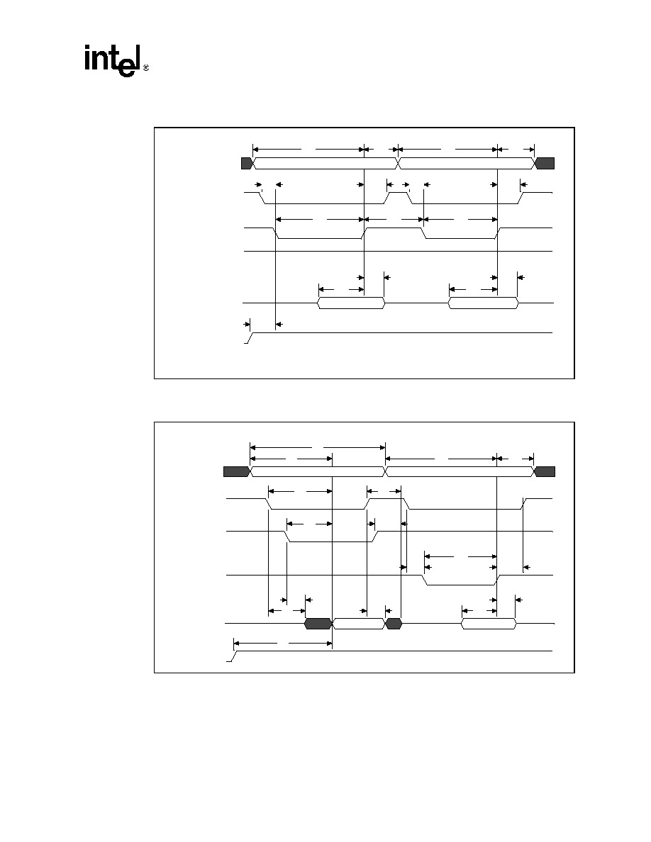
28F640K3, 28F640K18, 28F128K3, 28F128K18, 28F256K3, 28F256K18
Datasheet
51
Figure 16. Write to Write Waveform
W1
W7
W4
W7
W4
W3
W9
W3
W9
W3
W3
W6
W2
W6
W2
W8
W8
W5
W5
Address [A]
CE# [E}
WE# [W]
OE# [G]
Data [D/Q]
RST#/ RP# [P]
Figure 17. Asynchronous Read to Write Waveform
Q
D
R5
W7
W4
R10
R7
R6
W6
W3
W3
W2
R9
R4
R8
R3
W8
W5
R1
R2
R1
Address [A]
CE# [E}
OE# [G]
WE# [W]
Data [D/Q]
RST# [P]

28F640K3, 28F640K18, 28F128K3, 28F128K18, 28F256K3, 28F256K18
52
Datasheet
10.6
Block Erase and Program Operation Performance
Figure 18. Asynchronous Write to Read Waveform
Table 16. Block Erase and Program Operation Performance
#
Sym
Parameter
Notes
Min
Typ
Max
Unit
W0
t
WHQV1
, t
EHQV1
Write Buffer Program Time (Time to program 64 bytes/32 words)
4, 5, 6
320
960
µs
t
WHQV2
, t
EHQV2
Word Program Time (Using Word Program Command)
4
150
450
µs
t
WHQV3
, t
EHQV3
Block Program Time (Using Write-to- Buffer Command)
4
0.7
2.1
sec
t
BBWB
Buffered-EFP Buffer Write Time
1, 3, 4
288
864
µs
t
BWB
Buffered-EFP Block Write Time
1, 3, 4
0.58
1.7
sec
t
BEFP-SETUP
Buffered-EFP Set-up Time
1, 3, 4
N/A
5.0
µs
t
WHQV4
, t
EHQV4
Block Erase Time
4
1.0
4.0
sec
t
WHRH1
, t
EHRH1
Program Suspend Latency Time to Read
20
25
µs
t
WHRH
, t
EHRH
Erase Suspend Latency Time to Read
20
25
µs
WY
t
STS
STS Pulse Width Low Time
4
250
ns
NOTES:
1. Typical values measured at T
A
= +25
∞
C and nominal voltages. Assumes corresponding lock-bits are not set. Subject to change based on device
characterization.
2. These performance numbers are valid for all speed versions.
3. Sampled but not 100% tested.
4. Excludes system level overhead.
5. These values are valid when the buffer is full, and the start address is aligned on 32-bit boundary.
6. Effective word program time (t
WHQV1
, t
EHQV1
) is 10.0 µs/word (typ).
D
Q
W1
R9
R8
R4
R3
R2
W7
W4
W14
W18
W3
W3
R10
W6
W2
R1
R1
W8
W5
Address [A]
CE# [E}
WE# [W]
OE# [G]
Data [D/Q]
RST# [P]

28F640K3, 28F640K18, 28F128K3, 28F128K18, 28F256K3, 28F256K18
Datasheet
53
10.7
Reset Operation
Figure 19. Reset Operation Waveforms
(A) Reset during
read mode
(B) Reset during
program or block erase
P1
P2
(C) Reset during
program or block erase
P1
P2
V
IH
V
IL
V
IH
V
IL
V
IH
V
IL
RST# [P]
RST# [P]
RST# [P]
Abort
Complete
Abort
Complete
V
CC
0V
V
CC
(D) VCC Power-up to
RST# high
P1
R5
P2
P3
P2
R5
R5
RESET.WMF
Table 17. Reset Specifications
Num
Symbol
Parameter
Notes
Min
Max
Unit
P1
t
PLPH
RST# pulse width low
1,2,3,4
100
ns
P2
t
PLRH
RST# low to device reset during erase
1,3,4,7
20
µs
RST# low to device reset during program
1,3,4,7
10
P3
t
VCCPH
V
CC
Power Valid to RST# de-assertion (high)
1,4,5,6
60
NOTES:
1. These specifications are valid for all product versions (packages and speeds).
2. The device may reset if t
PLPH
is <t
PLPH
MIN, but this is not guaranteed.
3. Not applicable if RST# is tied to Vcc.
4. Sampled, but not 100% tested.
5. If RST# is tied to the V
CC
supply, device will not be ready until t
VCCPH
after V
CC
V
CC
min.
6. If RST# tied to any supply/signal with V
CCQ
voltage levels, the RST# input voltage must not exceed V
CC
until
V
CC
V
CC
(min).
7. Reset completes within t
PLPH
if RST# is asserted while no erase or program operation is executing.

28F640K3, 28F640K18, 28F128K3, 28F128K18, 28F256K3, 28F256K18
54
Datasheet
10.8
AC Test Conditions
NOTE:
AC test inputs are driven at V
CCQ
for Logic "1" and 0.0 V for Logic "0." Input/output timing begins or ends
at V
CCQ
/2. Input rise and fall times (10% to 90%) < 5 ns. Worst case speed occurs at V
CC
= V
CCMIN
.
NOTE:
C
L
included jig capacitance.
10.9
Capacitance
Figure 20. AC Input/Output Reference Waveform
IO_REF.WMF
Input V
CCQ
/2
V
CCQ
/2 Output
V
CCQ
0V
Test Points
Figure 21. Transient Equivalent Testing Load Circuit
Device
Under Test
R
2
R
1
V
CCQ
Out
C
L
LOAD_CKT.WMF
Table 18. Test Configuration Component Value for Worst Case Speed Conditions
Test Configuration
C
L
(pF)
R
1
R
2
V
CCQMIN
Standard Test
30
25K
25K
NOTE: C
L
includes jig capacitance.
Table 19. Capacitance
Sym
Parameter
(1)
Typ
Max
Unit
Condition
C
IN
Input Capacitance
6
8
pF
V
IN
= 0.0 V
C
OUT
Output Capacitance
8
12
pF
V
OUT
= 0.0 V
NOTES:
1. T
A
= +25∞C, f = 1 MHz.
2. Sampled, not 100% tested.

28F640K3, 28F640K18, 28F128K3, 28F128K18, 28F256K3, 28F256K18
Datasheet
55
Appendix A Write State Machine (WSM)
A.1
Nomenclature
Note: Numbered notes referenced in superscript can be found at the end of the last table.
Table 20. Arrangement Of Next State Table Pages
Next States
Cu
rre
n
t
S
t
at
es
Part A / page 1
Part B / page 1
Part A / page 2
Part B / Page 2
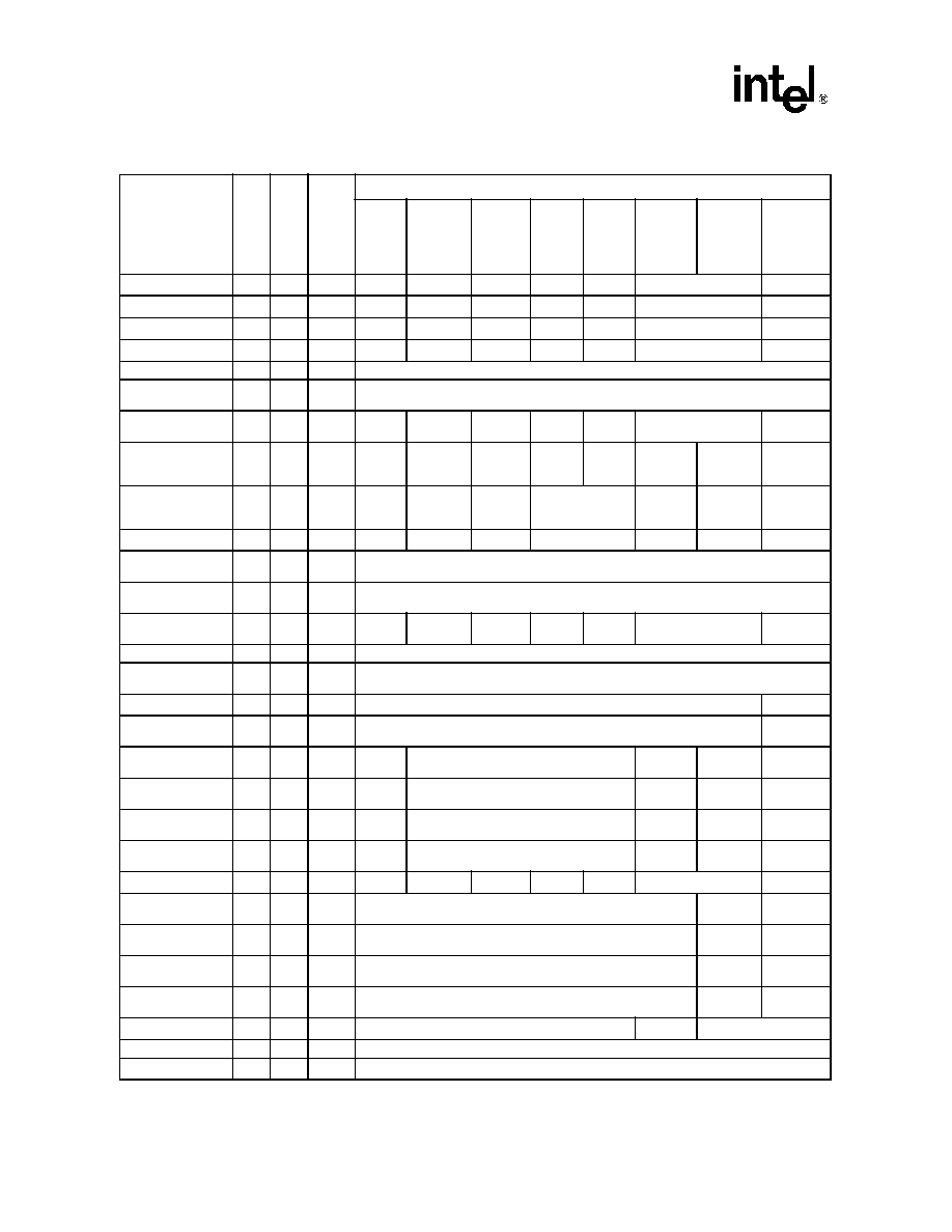
28F640K3, 28F640K18, 28F128K3, 28F128K18, 28F256K3, 28F256K18
56
Datasheet
Table 21. Next State Table Part A
Current State
SR7 SR0
Data
When
Read
Command Input and Next State
Read
Array
0xFF
Program
Setup
0x10/
0x40
Write to
Buffer
Setup
2,3
0xE8
BEFP
Setup
1
0x30
Erase
Setup
0x20
Erase/
BEFP/
Unlock
Confirm
7
0xD0
Program/
Erase
Confirm
7
0xD0
Program/
Erase
Suspend
5
0xB0
Read Array
1
0
Array
Read Array
Program Setup
Write to Buffer
Setup
BEFP Setup
Erase Setup
Read Array
Read Status
Read Status
1
0
Status
Read Array
Program Setup
Write to Buffer
Setup
BEFP Setup
Erase Setup
Read Array
Read Status
Read Config
1
0
Config
Read Array
Program Setup
Write to Buffer
Setup
BEFP Setup
Erase Setup
Read Array
Read Status
Read Query
1
0
CFI
Read Array
Program Setup
Write to Buffer
Setup
BEFP Setup
Erase Setup
Read Array
Read Status
Lock Setup
6
1
0
Status
Botch (command seq.error) if second cycle is anything other than 0xD0, 0x01, 0x2F, or 0x03
Lock Setup Erase
Susp
6
1
0
Status
Botch Erase Susp.(command seq. error) if second cycle is anything other than 0xD0, 0x01, 0x2F, or 0x03
Botch (command
seq. error)
9
1
0
Status
Read Array
Program Setup
Botch
BEFP Setup
Erase Setup
Read Array
Read Status
Botch Erase
Susp.(command
seq. error)
9
1
0
Status
Read Array
Ers. Susp.
Program Setup
Ers. Susp.
Botch Erase.
Susp.
Read Status
Ers. Susp.
Read Array
Ers. Susp.
Read Array
Ers.Susp.
Erase
Read Status
Ers. Susp.
Botch Prog.
Susp.(command
seq. error)
9
1
0
Status
Read Array
Prog. Susp.
Read Array
Prog. Susp.
Botch Prog.
Susp.
Read Array Prog. Susp.
Read Array
Prog. Susp.
Program (busy)
Read Status
Prog. Susp.
Botch Both Susp.
8
1
0
Status
Read Array
Both Susp.
Read Array Both
Susp.
Botch Both
Susp.
Read Array Both Susp.
Read Array
Both Susp.
Program (busy)
Ers. Susp.
Read Status
Both Susp.
OTP/Prot. Prog.
Setup
1
0
Status
OTP/Protection Register Program
OTP/Prot Prog.
(busy)
0
z
Status
OTP/Protection Register Program (busy)
OTP.Prot Prog.
(done)
1
0
Status
Read Array
Program Setup
Write to Buffer
Setup
BEFP Setup
Erase Setup
Read Array
Read Status
Prog. Setup
1
0
Status
Program (busy)
Prog. Setup Ers.
Susp.
1
0
Status
Program (busy) Ers. Susp.
Program (busy)
0
z
Status
Program (busy)
Read Status
Prog. Susp.
Program (busy)
Ers. Susp.
0
z
Status
Program (busy) Ers. Susp.
Read Status
Both Susp.
Read Status Prog.
Susp.
1
0
Status
Read Array
Prog. Susp.
Read Array Prog. Susp.
Read Array
Prog. Susp.
Program (busy)
Read Status
Prog. Susp.
Read Array Prog.
Susp.
1
0
Array
Read Array
Prog. Susp.
Read Array Prog. Susp.
Read Array
Prog. Susp.
Program (busy)
Read Status
Prog. Susp.
Read Config Prog.
Susp.
1
0
Config
Read Array
Prog. Susp.
Read Array Prog. Susp.
Read Array
Prog. Susp.
Program (busy)
Read Status
Prog. Susp.
Read Query Prog.
Susp.
1
0
CFI
Read Array
Prog. Susp.
Read Array Prog. Susp.
Read Array
Prog. Susp.
Program (busy)
Read Status
Prog. Susp.
Program (done)
1
0
Status
Read Array
Program Setup
Write to Buffer
Setup
BEFP Setup
Erase Setup
Read Array
Read Status
Read Status Both
Susp.
8
1
0
Status
Read Array Both Susp.
Program (busy)
Ers. Susp.
Read Status
Both Susp.
Read Array Both
Susp.
8
1
0
Array
Read Array Both Susp.
Program (busy)
Ers. Susp.
Read Status
Both Susp.
Read Config Both
Susp.
8
1
0
Config
Read Array Both Susp.
Program (busy)
Ers. Susp.
Read Status
Both Susp.
Read Query Both
Susp.
8
1
0
CFI
Read Array Both Susp.
Program (busy)
Ers. Susp.
Read Status
Both Susp.
BEFP Setup
1
0
Status
Botch (command seq. error)
BEFP Setup-
time
Botch (command seq. error)
BEFP Setup-time
0
1
Status
If Time-out > 5 us, go to BEFP Load; If Time-out < 5 us, stay in BEFP Setup-time
BEFP Load
0
0
Status
Initialize buffer load count to 31; if buffer count=0, then go to BEFP (busy); For buffer count>0 and same block addr. stay in BEFP Load; If
block addr. changed, go to BEFP exit

28F640K3, 28F640K18, 28F128K3, 28F128K18, 28F256K3, 28F256K18
Datasheet
57
BEFP (busy)
0
1
Status
To exit, change block addr; to continue proceed to BEFP after SR0=0.
BEFP Exit (Busy)
0
1
Status
Internally timed; Go to BEFP Exit after internal timeout; Transition indicated by SR0=0
BEFP Exit
1
0
Status
Read Array
Program Setup
Write to Buffer
Setup
BEFP Setup
Erase Setup
Read Array
Read Status
Write to Buffer
setup
1
0
Status
Repeat command until SR7=1. Next cycle will be interpreted as Count Load.
Count Load
1
0
Status
Word count load (Actual number of words-1). Lowest five bits will be assumed as the count. Device assumes next cycles will be Data
Load.
Data Load
1
0
Status
Data load; To quit or abort, change the block address during a write. The UI will botch on a block change. Repeat Data Load until Word
Count is reached, next command must be Write to Buffer Confirm
Write to Buffer
Confirm
1
0
Status
Botch (command seq. error)
Program (busy)
Botch (command seq. error)
Write to Buffer
setup Ers. Susp.
1
0
Status
Repeat command until SR7=1. Next cycle will be interpreted as Count Load Ers. Susp..
Count Load Ers.
Susp.
1
0
Status
Word count load (Actual number of words-1). Lowest five bits will be assumed as the count. Device assumes next cycles will be Data Load
Ers. Susp..
Data Load Ers.
Susp.
1
0
Status
Data load; To quit or abort, change the block address during a write. The UI will botch on a block change. Repeat Data Load until Word
Count is reached, next command must be Write to Buffer Confirm Ers. Susp.
Write to Buffer
confirm Ers. Susp.
1
0
Status
Botch Ers. Susp.(command seq. error)
Program (busy)
Ers. Susp.
Botch Ers. Susp.(command seq.
error)
Erase Setup
1
0
Status
Botch (command seq. error
Erase (busy)
Botch (command
seq. error)
Erase (busy)
0
z
Status
Erase (busy)
Read Status Ers.
Susp.
1
0
Status
Read Array
Ers. Susp.
Program Setup
Ers. Susp.
Write to Buffer
Setup Ers.
Susp.
Read Status
Ers. Susp.
Read Array
Ers. Susp.
Read Array Ers.
Susp.
Erase (busy)
Read Status Ers.
Susp.
Read Array Ers.
Susp.
1
0
Array
Read Array
Ers. Susp
Program Setup
Ers. Susp.
Write to Buffer
Setup Ers.
Susp
Read Array
Ers. Susp.
Read Array
Ers. Susp
Read Array Ers.
Susp.
Erase (busy)
Read Status Ers.
Susp.
Read Config Ers.
Susp.
1
0
Config
Read Array
Ers. Susp
Program Setup
Ers. Susp.
Write to Buffer
Setup Ers.
Susp
Read Array
Ers. Susp
Read Array
Ers. Susp
Read Array Ers.
Susp.
Erase (busy)
Read Status Ers.
Susp.
Read Query Ers.
Susp.
1
0
CFI
Read Array
Ers. Susp
Program Setup
Ers. Susp.
Write to Buffer
Setup Ers.
Susp
Read Array
Ers. Susp
Read Array
Ers. Susp
Read Array Ers.
Susp.
Erase (busy)
Read Status Ers.
Susp.
Erase (done)
1
0
Status
Read Array
Program Setup
Write to Buffer
Setup
BEFP Setup
Erase Setup
Read Array
Read Status
STS Reconfig
Setup
1
0
Status
If second cycle is 0x00 or 0x01 or 0x02 or 0x03, then reconfigure the STS functionality and go to Read Status; If not Botch.
STS Reconfig
Setup Ers. Susp.
1
0
Status
If second cycle is 0x00 or 0x01 or 0x02 or 0x03, then reconfigure the STS functionality and go to Read Status Ers. Susp; If not Botch Ers.
Susp.
STS Reconfig
Setup Prog. Susp.
1
0
Status
If second cycle is 0x00 or 0x01 or 0x02 or 0x03, then reconfigure the STS functionality and go to Read Status Prog.Susp; If not Botch
Prog. Susp.
STS Reconfig
Setup Both Susp.
1
0
Status
If second cycle is 0x00 or 0x01 or 0x02 or 0x03, then reconfigure the STS functionality and go to Read Status Both Susp; If not Botch Both
Susp.
Table 21. Next State Table Part A
Current State
SR7 SR0
Data
When
Read
Command Input and Next State
Read
Array
0xFF
Program
Setup
0x10/
0x40
Write to
Buffer
Setup
2,3
0xE8
BEFP
Setup
1
0x30
Erase
Setup
0x20
Erase/
BEFP/
Unlock
Confirm
7
0xD0
Program/
Erase
Confirm
7
0xD0
Program/
Erase
Suspend
5
0xB0

28F640K3, 28F640K18, 28F128K3, 28F128K18, 28F256K3, 28F256K18
58
Datasheet
Table 22. Next State Table Part B
Current State
SR7 SR0
Data
When
Read
Command Input and Next State
Read
Status
0x70
Clear
Status
4
0x50
Read
Config
0x90
STS Re-
config
0xB8
Read
Query
0x98
Lock
Setup
0x60
OTP/Prot
Program
Setup
0xC0
Illegal
Commands
Read Array
1
0
Array
Read Status
Read Array
Read Config
STS Reconfig
Setup
Read Query
Lock Setup
OTP/Prot Prog.
Setup
Read Array
Read Status
1
0
Status
Read Status
Read Array
Read Config
STS Reconfig
Setup
Read Query
Lock Setup
OTP/Prot Prog.
Setup
Read Array
Read Config
1
0
Config
Read Status
Read Array
Read Config
STS Reconfig
Setup
Read Query
Lock Setup
OTP/Prot Prog.
Setup
Read Array
Read Query
1
0
CFI
Read Status
Read Array
Read Config
STS Reconfig
Setup
Read Query
Lock Setup
OTP/Prot Prog.
Setup
Read Array
Lock Setup
6
1
0
Status
Botch(command seq.error) if second cycle is anything other than 0xD0, 0x01, 0x2F, or 0x03
Lock Setup
Erase Susp
6
1
0
Status
Botch Erase Susp.(command seq. error) if second cycle is anything other than 0xD0, 0x01, 0x2F, or 0x03
Botch (command
seq. error)
9
1
0
Status
Read Status
Read Array
Read Config
STS Reconfig
Setup
Read Query
Lock Setup
OTP/Prot Prog.
Setup
Read Array
Botch Erase
Susp.(command
seq. error)
9
1
0
Status
Read Status
Ers. Susp.
Read Array Ers.
Susp.
Read Config
Ers. Susp.
STS Reconfig
Setup
Ers.Susp.
Read Query
Ers. Susp.
Lock Setup
Ers. Susp.
Read Array Ers.
Susp.
Read Array
Botch Prog.
Susp.(command
seq. error)
9
1
0
Status
Read Status
Prog. Susp.
Read Array
Prog. Susp.
Read Config
Prog Susp.
STS Reconfig
Setup Prog
Susp.
Read Query
Prog. Susp.
Read Array Prog. Susp
Read Array Prog
Susp.
Botch Both
Susp.
8
1
0
Status
Read Status
Both Susp.
Read Array Both
Susp.
Read Config
Both Susp.
STS Reconfig
Setup Both
Susp.
Read Query
Both Susp.
Read Array Both Susp.
Read Array Both
Susp.
OTP/Prot. Prog.
Setup
1
0
Status
OTP/Protection Register
Program
OTP/Prot Register Program
OTP/Prot Prog.
(busy)
0
z
Status
OTP/Protection Register
Program (busy)
OTP/Prot Register Program (busy)
OTP.Prot Prog.
(done)
1
0
Status
Read Status
Read Array
Read Config
STS Reconfig
Setup
Read Query
Lock Setup
OTP/Prot Prog.
Setup
Read Array
Prog. Setup
1
0
Status
Program (busy)
Prog. Setup Ers.
Susp.
1
0
Status
Program (busy) Ers. Susp.
Program (busy)
0
z
Status
Program (busy)
Program (busy)
Ers. Susp.
0
z
Status
Program (busy) Ers. Susp.
Read Status
Prog. Susp.
1
0
Status
Read Status
Prog. Susp.
Read Array Prog
Susp.
Read Config
Prog. Susp.
STS Reconfig
Setup Prog.
Susp.
Read Query
Prog Susp.
Read Array Prog. Susp.
Read Array Prog.
Susp.
Read Array
Prog. Susp.
1
0
Array
Read Status
Prog. Susp.
Read Array Prog
Susp.
Read Config
Prog. Susp.
STS Reconfig
Setup Prog.
Susp.
Read Query
Prog Susp.
Read Array Prog. Susp.
Read Array Prog.
Susp.
Read Config
Prog. Susp.
1
0
Config
Read Status
Prog. Susp.
Read Array Prog
Susp.
Read Config
Prog. Susp.
STS Reconfig
Setup Prog.
Susp.
Read Query
Prog Susp.
Read Array Prog. Susp.
Read Array Prog.
Susp.
Read Query
Prog. Susp.
1
0
CFI
Read Status
Prog. Susp.
Read Array Prog
Susp.
Read Config
Prog. Susp.
STS Reconfig
Setup Prog.
Susp.
Read Query
Prog Susp.
Read Array Prog. Susp.
Read Array Prog.
Susp.
Program (done)
1
0
Status
Read Status
Read Array
Read Config
STS Reconfig
Setup
Read Query
Lock Setup
Prot. Prog. Setup
Read Array
Read Status
Both Susp.
8
1
0
Status
Read Status
Both Susp.
Read Array Both
Susp.
Read Config
Both Susp.
STS Reconfig
Setup Both
Susp.
Read Query
Both Susp.
Read Array Both Susp
Read Array Both
Susp.
Read Array Both
Susp.
8
1
0
Array
Read Status
Both Susp.
Read Array Both
Susp.
Read Config
Both Susp.
STS Reconfig
Setup Both
Susp.
Read Query
Both Susp.
Read Array Both Susp
Read Array Both
Susp.
Read Config
Both Susp.
8
1
0
Config
Read Status
Both Susp.
Read Array Both
Susp.
Read Config
Both Susp.
STS Reconfig
Setup Both
Susp.
Read Query
Both Susp.
Read Array Both Susp
Read Array Both
Susp.
Read Query
Both Susp.
8
1
0
CFI
Read Status
Both Susp.
Read Array Both
Susp.
Read Config
Both Susp.
STS Reconfig
Setup Both
Susp.
Read Query
Both Susp.
Read Array Both Susp
Read Array Both
Susp.
BEFP Setup
1
0
Status
Botch (command sequence error)
BEFP Setup-
time
0
1
Status
If Time-out> 5us, go to BEFP Load; If Time-out<5us, stay in BEFP Setup-time
BEFP Load
0
0
Status
Initialize buffer load count to 31; if buffer count=0, then go to BEFP (busy); For buffer count>0 and same block addr. stay in BEFP Load; If
block addr. changed, go to BEFP exit

28F640K3, 28F640K18, 28F128K3, 28F128K18, 28F256K3, 28F256K18
Datasheet
59
BEFP (busy)
0
1
Status
To exit, change block addr; to continue proceed to BEFP after SR0=0.
BEFP Exit
(Busy)
0
1
Status
Internally timed; Go to BEFP Exit after internal timeout; Transition indicated by SR0=0
BEFP Exit
1
0
Status
Read Status
Read Array
Read Config
STS Reconfig
Setup
Read Query
Lock Setup
Prot. Prog. Setup
Read Array
Write to Buffer
setup
1
0
Status
Repeat command until SR7=1. Next cycle will be interpreted as Count Load.
Count Load
1
0
Status
Word count load (Actual number of words-1). Lowest five bits will be assumed as the count. Device assumes next cycles will be Data Load.
Data Load
1
0
Status
Data load; To quit or abort, change the block address during a write. The UI will botch on a block change. Repeat Data Load until Word Count
is reached, next command must be Write to Buffer Confirm
Write to Buffer
Confirm
1
0
Status
Botch (command sequence error)
Write to Buffer
setup Ers. Susp.
1
0
Status
Repeat command until SR7=1. Next cycle will be interpreted as Count Load Ers. Susp..
Count Load Ers.
Susp.
1
0
Status
Word count load (Actual number of words-1). Lowest five bits will be assumed as the count. Device assumes next cycles will be Data Load
Ers. Susp..
Data Load Ers.
Susp.
1
0
Status
Data load; To quit or abort, change the block address during a write. The UI will botch on a block change. Repeat Data Load until Word Count
is reached, next command must be Write to Buffer Confirm Ers. Susp.
Write to Buffer
confirm Ers.
Susp.
1
0
Status
Botch Ers. Susp. (command sequence error)
Erase Setup
1
0
Status
Botch (command sequence error)
Erase (busy)
0
z
Status
Erase (busy)
Read Status Ers.
Susp.
1
0
Status
Read Status
Ers. Susp.
Read Array Ers.
Susp.
Read Config
Ers. Susp.
STS Reconfig
Setup Ers.
Susp.
Read Query
Ers. Susp.
Lock Setup
Ers. Susp.
Read Array Ers.
Susp.
Read Array Ers.
Susp.
Read Array Ers.
Susp.
1
0
Array
Read Status
Ers. Susp.
Read Array Ers.
Susp.
Read Config
Ers. Susp.
STS Reconfig
Setup Ers.
Susp.
Read Query
Ers. Susp.
Lock Setup
Ers. Susp.
Read Array Ers.
Susp.
Read Array Ers.
Susp.
Read Config
Ers. Susp.
1
0
Config
Read Status
Ers. Susp.
Read Array Ers.
Susp.
Read Config
Ers. Susp.
STS Reconfig
Setup Ers.
Susp.
Read Query
Ers. Susp.
Lock Setup
Ers. Susp.
Read Array Ers.
Susp.
Read Array Ers.
Susp.
Read Query Ers.
Susp.
1
0
CFI
Read Status
Ers. Susp.
Read Array Ers.
Susp.
Read Config
Ers. Susp.
STS Reconfig
Setup Ers.
Susp.
Read Query
Ers. Susp.
Lock Setup
Ers. Susp.
Read Array Ers.
Susp.
Read Array Ers.
Susp.
Erase (done)
1
0
Status
Read Status
Read Array
Read Config
STS Reconfig
Setup
Read Query
Lock Setup
Prot. Prog. Setup
Read Array
STS Reconfig
Setup
1
0
Status
If second cycle is 0x00 or 0x01 or 0x02 or 0x03, then reconfigure the STS functionality and go to Read Status; If not Botch.
STS Reconfig
Setup Ers. Susp.
1
0
Status
If second cycle is 0x00 or 0x01 or 0x02 or 0x03, then reconfigure the STS functionality and go to Read Status Ers. Susp; If not Botch Ers.
Susp.
STS Reconfig
Setup Prog.
Susp.
1
0
Status
If second cycle is 0x00 or 0x01 or 0x02 or 0x03, then reconfigure the STS functionality and go to Read Status Prog.Susp; If not Botch Prog.
Susp.
STS Reconfig
Setup Both
Susp.
1
0
Status
If second cycle is 0x00 or 0x01 or 0x02 or 0x03, then reconfigure the STS functionality and go to Read Status Both Susp; If not Botch Both
Susp.
NOTES:
1. For BEFP, the block address should be changed only when the buffer is full.
2. Start address is the address loaded during the Count Load cycle.
3. The Write to Buffer command is invalid when a botch has occurred. The status register should be cleared before issuing the Write to Buffer command.
4. A Clear Status Register command is allowed during erase or program suspend.
5. When a suspend command is issued while the device is busy (program or erase), the device will not enter suspend until the appropriate suspend latency has elapsed.
Any additional commands issued during this latency interval will cause indeterminate results.
6. When the lock/write RCR operation is complete, the device returns to Read Status mode. If the Lock Setup command is issued during Erase Suspend, the the device
will revert to Read Status Ers. Susp.
7. The Confirm command (0xD0) is interpreted as the second cycle of a two-cycle command while a Resume command 0xD0 is interpreted as a stand-alone, single-cycle
command. The device will not resume from suspend when the command sequence 0x20, 0xD0 is issued while in suspend state.
8. Both Suspend indicates a Program Suspend nested within an Erase Suspend.
9. A Botch state is indicated when status bits SR4 and SR5 are set, and is the result of an invalid command sequence. The Clear Status Register command (0x50)must
be issued to continue.
Table 22. Next State Table Part B
Current State
SR7 SR0
Data
When
Read
Command Input and Next State
Read
Status
0x70
Clear
Status
4
0x50
Read
Config
0x90
STS Re-
config
0xB8
Read
Query
0x98
Lock
Setup
0x60
OTP/Prot
Program
Setup
0xC0
Illegal
Commands

28F640K3, 28F640K18, 28F128K3, 28F128K18, 28F256K3, 28F256K18
60
Datasheet
Appendix B Common Flash Interface
B.1
Query Structure Overview
The Query command causes the flash component to display the Common Flash Interface (CFI)
Query structure or "database." The structure sub-sections and address locations are summarized
below. For further details see AP-646 Common Flash Interface (CFI) and Command Sets (Order
No 292204) for a full description of CFI.
B.2
CFI Query Identification String
The Identification String provides verification that the component supports the Common Flash
Interface specification. It also indicates the specification version and supported vendor-specified
command set(s).
Table 23. Query Structure
(1)
Offset
Sub-Section Name
Description
00000h
0089
Manufacturer Code
00001h
Device Code
(BA+2)h
(2)
Block Status Register
Block-specific information
000(04 -0F)h
Reserved
Reserved for vendor-specific
information
00010h
CFI Query Identification String
Command set ID and vendor data
offset
0001Bh
System Interface Information
Device timing & voltage information
00027h
Device Geometry Definition
Flash device layout
P
(3)
Primary Intel
-
Specific Extended Query
Table
Vendor
-
defined additional information
specific to the Primary Vendor
Algorithm
NOTES:
1. Refer to the Query Structure Output section and offset 28h for the detailed definition of offset address as a function of device
bus width and mode.
2. BA = The beginning location of a Block Address (e.g., 010000h is the beginning location of block 1 when the block size is 64
Kword).
3. Offset 15 defines "P" which points to the Primary Intel
-
specific Extended Query Table.

28F640K3, 28F640K18, 28F128K3, 28F128K18, 28F256K3, 28F256K18
Datasheet
61
B.3
System Interface Information
The following tables give information on the power supplies and the program and erase time
details as output by the device when the system software requests System Interface Information.
The values stored are available from an offset address of 1Bh.
Table 24. CFI Identification
Offset
Length
Description
Addr.
Hex
Code
Value
10h
3
Query-unique ASCII string "QRY"
10
--51
"Q"
11:
--52
"R"
12:
--59
"Y"
13h
2
Primary vendor command set and control interface ID code.
13:
--01
16-bit ID code for vendor-specified algorithms
14:
--00
15h
2
Extended Query Table primary algorithm address
15:
--31
16:
--00
17h
2
Alternate vendor command set and control interface ID code
17:
--00
0000h means no second vendor-specified algorithm exists
18:
--00
19h
2
Secondary algorithm Extended Query Table address.
19:
--00
0000h means none exists
1A:
--00
Table 25. System Interface Information
Offset
Length
Description
Addr.
Hex
Code
Value
1Bh
1
V
CC
logic supply minimum program/erase voltage
bits 0≠3 BCD 100 mV
bits 4≠7 BCD volts
1B:
--27
2.7 V
1Ch
1
V
CC
logic supply maximum program/erase voltage
bits 0≠3 BCD 100 mV
bits 4≠7 BCD volts
1C:
--36
3.6 V
1Dh
1
V
PP
[programming] supply minimum program/erase voltage
bits 0≠3 BCD 100 mV
bits 4≠7 HEX volts
1D:
--00
0.0 V
1Eh
1
V
PP
[programming] supply maximum program/erase voltage
bits 0≠3 BCD 100 mV
bits 4≠7 HEX volts
1E:
--00
0.0 V
1Fh
1
"n" such that typical single word program time-out = 2
n
µs
1F:
--08
256 µs
20h
1
"n" such that typical buffer write time-out = 2
n
µs
20:
--09
512 µs
21h
1
"n" such that typical block erase time-out = 2
n
ms
21:
--0A
1 s
22h
1
"n" such that typical full chip erase time-out = 2
n
ms
22:
--00
n/a
23h
1
"n" such that maximum word program time-out = 2
n
times typical
23:
--01
512 µs
24h
1
"n" such that maximum buffer write time-out = 2
n
times typical
24:
--01
1024 µs
25h
1
"n" such that maximum block erase time-out = 2
n
times typical
25:
--02
4 s
26h
1
"n" such that maximum chip erase time-out = 2
n
times typical
26:
--00
NA

28F640K3, 28F640K18, 28F128K3, 28F128K18, 28F256K3, 28F256K18
62
Datasheet
B.4
Device Geometry Definition
The following tables give critical details provided by CFI when the software requests flash device
geometry information such as the size of the device, types of read interfaces, program buffer size
etc.,
Table 26. Device Geometry Definition
Offset
Length
Description
Address
Hex Value
Meaning
27h
1
"n" such that the device size = 2
n
in number of
bytes
27:
See Table Below
28h
2
Flash Device Interface Code assignments:
28:
29:
--01
--00
x16
2Ah
2
"n" such that maximum number of bytes in
write buffer=2
n
2A:
2B:
--06
--00
64
2Ch
1
Number of Erase Blocks Within the Device:
1. x=0 means no erase blocking; the device
erases in "bulk"
2. x specifies the number of device or partition
regions with one or more contiguous same-
size erase blocks
3. Array size = (total blocks) x (individual
blocks size)
--01
1
2Dh
4
Erase Block Region Information
bits 0-15=y, y+1 = number of identical-size
erase blocks
bits 16-31=z, region erase block(s) size are z
x 256 bytes
2D:
See Table Below
2E:
2F:
00
30:
02
--
--
--
--
x64
x32
x16
x8
15
14
13
12
11
10
9
8
--
--
--
--
--
--
--
--
Table 46a. No of Erase blocks and Erase block region information
Address
64 Mbit
128 Mbit
256 Mbit)
27 h
17h
18h
19h
2D h
3Fh
7Fh
FFh
2E h
00h
00h
00h
28F640K3, 28F640K18, 28F128K3, 28F128K18, 28F256K3, 28F256K18
Datasheet
63
B.5
Primary Vendor Specific Extended Query Table
Certain flash features and commands are optional. The Primary Vendor Specific Extended Query
Table specifies this and other similar information.
Table 27. Primary Vendor Specific Extended Query Table
Offset
(1)
P=31h
Length
Description
(Optional Flash Features and Commands)
Add
Hex
Code
Value
(P+0)h
3
Primary Extended Query Table Unique ASCII
String "PRI"
31:
--50
"P"
(P+1)h
32:
--52
"R"
(P+2)h
33:
--49
"I"
(P+3)h
1
Major version number, ASCII
34:
--31
"1"
(P+4)h
1
Minor version number, ASCII
35:
--31
"1"
(P+5)h
(P+6)h
(P+7)h
(P+8)h
4
Optional feature and command support(1=yes,
0=no) bits 11-31 are reserved; undefined bits are
"0". If bit 31 is "1" then another 31 bit field of
optional features follows at the end of the 30-bit
field.
bit 0 - Chip Erase Supported
bit 1 - Suspend Erase Supported
bit 2 -Suspend Program Supported
bit 3 - Legacy lock/unlock Supported
bit 4 - Queued Erase Supported
bit 5 - Instant Individual Block Locking Supported
bit 6 - Protection Bits Supported
bit 7 - Page-mode read supported
bit 8 - Synchronous Read Supported
bit 9 - Simultaneous Operations Supported
bit 10 - Feature space Supported
36:
--E6
37:
--01
38:
--00
39:
--00
bit 0 = 0
No
bit 1 = 1
Yes
bit 2 = 1
Yes
bit3 = 0
No
bit 4 = 0
No
bit 5= 1
Yes
bit 6= 1
Yes
bit 7= 1
Yes
bit 8 = 1
Yes
bit 9 = 0
No
bit 10 =0
No
(P+9)h
1
Supported Functions After Suspend: Read Array,
Status, Query
Other Supported Operations are:
bits 1-7 reserved; undefined bits are "0"
bit 0 Program supported after erase suspend
3A:
--01
01
bit 0=1
Yes

28F640K3, 28F640K18, 28F128K3, 28F128K18, 28F256K3, 28F256K18
64
Datasheet
(P+A)h
(P+B)h
2
Block Status Register Mask
bits 3 -15 are reserved; undefined bits are "0"
bit 0 Block Lock-bit status register bit active
bit 1 Block Lock down bit status active
bit 2 Unlock down bit
3B:
--07
3C:
--00
bit 0 = 1
Yes
bit 1 = 1
Yes
(P+C)h
1
Vcc logic supply highest performance program/
erase voltage
bits 0-3 BCD value in 100mV
bits 4-7 BCD value in Volts
3D:
--33
3.3
(P+D)h
1
Vpp optimum program/erase supply voltage
bits 0-3 BCD value in 100mV
bits 4-7 Hex value in Volts
3E:
--00
--0.0V
Table 28. Protection Register Information
Offset
(1)
P=31h
Length
Description(Optional Flash Features and
Commands)
Add
Hex
Code
Value
(P+E)h
1
Number of Protection register fields in JEDEC ID space.
"00h", indicates that 256 protection fields are available
3F:
--02
02
(P+F)h,
(P+10)h,
(P+11)h,
(P+12)h
4
Protection field 1: Protection description
This field describes user-available One Time Program-
mable(OTP) protection register bytes. Some are pre-
programmed with device-unique serial numbers. Others
are user-programmable. Bits 0-15 point to the protection
register lock byte, the section's first byte. The following
bytes are factory pre-programmed and user-program-
mable
bits 0-7 = Lock/bytes JEDEC-plane physical low address
bits 8-15 =Lock/bytes JEDEC-plane physical high address
bits 16-23 = "n" such that 2
n
= factory pre-programmed
bytes
bits 24-31 = "n" such that 2
n
= user-programmable bytes
40:
41:
42:
43:
--80
--00
--03
--03
80h
00h
8 bytes
8 bytes
(P+13)h,
(P+14)h,
(P+15)h,
(P+16)h,
(P+17)h,
(P+18)h,
(P+19)h,
(P+1A)h,
(P+1B)h,
(P+1C)h
10
Protection field 2: Protection description
Bits 0-31 = point to the protection register physical Lock-
word address in the Jedec-plane.
Following bytes are factory or user-programmable
Bits 32-39 ="n"-factory pgm'd groups(low byte)
Bits 40-47="n"-factory pgm'd groups(high byte)
bits 48-55 ="n" such that 2
n
=factory programmable bytes
per group
bits 56-63="n"-user pgm'd groups(low byte)
bits 64-71="n"-user pgm'd groups(high byte)
bits 72-79="n" such that 2
n
= user programmable bytes/
group
44:
45:
46:
47:
48:
49:
4A:
4B:
4C:
4D:
--89
--00
--00
--00
--00
--00
--00
--10
--00
--04
89h
00h
00h
00h
0
0
0
16
0
16
NOTE:
The variable P is a pointer which is defines at CFI offset 15h.
Table 27. Primary Vendor Specific Extended Query Table
Offset
(1)
P=31h
Length
Description
(Optional Flash Features and Commands)
Add
Hex
Code
Value

28F640K3, 28F640K18, 28F128K3, 28F128K18, 28F256K3, 28F256K18
Datasheet
65
Table 29. Burst/Page Read Information
Offset
(1)
P=31h
Length
Description(Optional Flash Features and
Commands)
Add
Hex
Code
Value
(P+1D)h
1
Page Mode Read Capability
bits 0-7="n" such that 2
n
HEX value represents the
number of read page bytes. See offset 28h for
device word width to determine page mode data
output width. 00h indicates no read page buffer.
4E:
--04
16 bytes
(P+1E)h
1
Number of synchronous mode read configuration
fields that follow. 00h indicates no burst capability
4F:
--02
2
(P+1F)h
1
Synchronous Mode Read Capability Configuration 1
Bits 3-7 = Reserved
bits 0-2 = "n" such that 2
n+1
HEX value represents
the maximum number of continuous synchronous
burst reads when the device is configured for its
maximum word width. A value of 07h indicates that
the device is capable of continuous linear bursts until
that will output data until the internal burst counter
reaches the end of the device's burstable address
space. This field's 3-bit value can be written directly
to the Read Configuration Register Bits 0-2 if the
device is configured for its maximum word width.
See offset 28h for word width to determine the burst
data output width.
50:
--02
8
(P+20)h
1
Synchronous Mode Read Capability Configuration 2
51:
--03
16

28F640K3, 28F640K18, 28F128K3, 28F128K18, 28F256K3, 28F256K18
66
Datasheet
Appendix C Flowcharts
Figure 22. Write to Buffer Flowchart
Start
Get Next
Target Address
Issue Write to Buffer
Command 0xE8 and
Block Address
Read Extended
Status Register
(at Block Address)
Is Buffer
Available?
XSR.7 =
Full Status
Check if Desired
Programming
Complete
1. Word count values on DQ
7
-DQ
0
are loaded into the Count
register. Count ranges for this device are N = 0x00 to 0x1F.
2. The device outputs the status register when read (XSR is no
longer available).
3. Write Buffer contents will be programmed at the device start
address or destination flash address.
4. Align the start address on a Write Buffer boundary for
maximum programming performance (i.e., A
5
≠A
1
of the start
address = 0).
5. The device aborts the Write to Buffer command if the current
address is outside the original block address.
6. The Status register indicates an "improper command
sequence" if the Write to Buffer command is aborted. Follow
this with a Clear Status Register command.
Full status check can be done after all erase and write
sequences complete. Write 0xFF after the last operation to reset
the device to read array mode.
1 = Yes
Device
Supports Buffer
Writes?
Set Time-out or
Loop Counter
Time-out
or Count
Expired?
Write Confirm 0xD0
and Block Address
Another Write
to Buffer?
Read Status Register
SR.7 = ?
0
1
Yes
No
Bus
Operation
Standby
Read
Command
No
Write
Write to
Buffer
Read
Standby
Comments
Check SR.7
1 = WSM Ready
0 = WSM Busy
Status register Data
Transition to V
IL
of either CE# or
OE# updates SR
Addr = Block Address
Data = 0xE8
Addr = Block Address
XSR.7 = Valid
Addr = Block Address
Check XSR.7
1 = Write Buffer available
0 = No Write Buffer available
Write
Write
Confirm
Data = 0xD0
Addr = Block Address
Write Buffer Data,
Start Address
X = 0
Yes
0 = No
No
Issue Read Status
Register Command
Yes
Use Single Word
Programming
Abort Write
to Buffer?
No
X = N?
Write Buffer Data,
Block Address
X = X + 1
Write to another
Block Address
Write to Buffer Aborted
No
Yes
Yes
Write
(Notes 1, 2)
Data = N = W ord Count
N = 0 corresponds to count = 1
Addr = Block Address
Write
(Notes 3, 4)
Data = Write Buffer Data
Addr = Start Address
Write Word Count,
Block Address
Write
(Notes 5, 6)
Data = Write Buffer Data
Addr = Block Address

28F640K3, 28F640K18, 28F128K3, 28F128K18, 28F256K3, 28F256K18
Datasheet
67
Figure 23. Word Programming Flowchart
Suspend
Program
Loop
Start
Write 0x40,
Address
Write Data and
Address
Read Status Register
SR.7 =?
Full Status
Check if Desired
Program Complete
FULL STATUS CHECK PROCEDURE
Repeat for subsequent programming operations.
SR full status check can be done after each program or after a
sequence of program operations.
Write 0xFF after the last program operation to read array mode.
Suspend
Program
Comments
Data = 0x40
Addr = Location to Program
Data = Data to Program
Addr = Location to Program
Read Status Register
Data (See Above)
V
PEN
Range Error
Device Protect Error
Program Successful
SR.3 =
SR.1 =
0
0
Program Error
SR.4 =
0
Bus Operation
Write
Write
Command
W ord Program
Setup
Data
Status Register Data. Toggle
CE# or OE# to Update Status
Register Data
Read
Check SR.7
1 = WSM Ready
0 = WSM Busy
Standby
1
1
1
1
0
Yes
No
WORD PROGRAM PROCEDURE
SR.3 MUST be cleared before further attempts are allowed by the
W rite State Machine If set during a program attempt
SR.4, SR.3 and SR.1 are only cleared by the Clear Staus Register
command in cases where multiple locations are programmed before
full status is checked.
If an error is detected, clear the status register before attempting retry
or other error recovery.
Comments
Check SR.3
1 = V
PEN
Error Detect
Check SR.1
1 = Attempted Program to
Locked Block - Program
aborted
Check SR.4
1 = Data Program Error
Bus Operation
Standby
Standby
Standby
Command

28F640K3, 28F640K18, 28F128K3, 28F128K18, 28F256K3, 28F256K18
68
Datasheet
Figure 24. Program Suspend/Resume Flowchart
Start
Write 0xB0
Read Status Register
Comments
Data = 0xB0
Addr = X
Data = 0xFF
Addr = X
SR.7 =
SR.2 =
Write 0xFF
Read Array Data
Program Completed
Done
Reading
Write 0xFF
Write 0xD0
Program Resumed
Read Array Data
Read array data from block
other than the one being
programmed.
Check SR.7
1 = WSM Ready
0 = WSM Busy
Check SR.2
1 = Program Suspended
0 = Program Completed
Data = 0xD0
Addr = X
Bus
Operation
Write
Write
Read
Read
Standby
Standby
Write
Command
Program
Suspend
Read Array
Program
Resume
Status Register Data; Toggle
CE# or OE# to Update Status
Register Data
Addr = X
Program
Suspend
Read Array
Program
Resume
0
No
0
Yes
1
1

28F640K3, 28F640K18, 28F128K3, 28F128K18, 28F256K3, 28F256K18
Datasheet
69
Figure 25. Buffered Enhanced Factory Programming Procedure Flowchart
SR
.
0
=
1
=
N
Write Data
Address = WA
0
Last
Data?
Write FFFFh
Address = other
block
Program
Done?
Read
Status Register
SR.0=0=Y
Y
SR.7=0=N
Full Status Check
Procedure
Program
Complete
Read
Status Register
BEFP
Exited?
SR.7=1=Y
Start
Write 80h
Address = WA
0
Unlock
Block
Write D0h
Address = WA
0
BEFP Setup
Done?
Read
Status Register
SR.7=1=N
Exit
N
BEFP Program & Verify
BEFP Exit
BEFP Setup
Check
X = 32?
Initialize count
X = 0
Increment count
X = X+1
Y
NOTES:
1. WA
0
= first word address to be
programmed within the target block. WA
0
must align on a write buffer boundary.
2. The status register is updated when a
system read toggles OE# low-high-low.
3. Write buffer contents are programmed
sequentially to the flash array starting at
WA
0
. The WSM internally increments
addressing.
N
Check V
PEN
& Lock
errors (SR.3, SR.1)
SR.7=0=Y
BEFP Setup
Comments
Bus
State
Write
(note 1)
BEFP
Setup
Write
BEFP
Confirm
Read
(note 2)
Standby
BEFP
Setup
Done?
Write
Unlock
Block
Data = 80h
Address = WA
0
Data = D0h
Address = WA
0
Status Register
Address = WA
0
Check SR.7
0 = BEFP ready
1 = BEFP not ready
Unlock block
Standby
Error
Condition
Check
If SR.7 = 1:
Check SR.3, SR.1
SR.3 = 1 = V
PEN
error
SR.1 = 1 = locked block
BEFP Program & Verify
Comments
Bus
State
Write
(note 3)
Standby
Inc.
Count
Standby
Initialize
Count
Data = word to program
Address = WA
0
X = X+1
X = 0
Comments
Bus State
Standby
Buffer
Full?
X = 32?
If yes, read SR.0
If no, load next data word
BEFP Setup time
Data Stream
Ready?
Read
Status Register
SR.0=0=Y
SR.0=1=N
Read
Standby
Data
Stream
Ready?
Status Register
Address = WA
0
Check SR.0
0 = Ready for data
1= Not ready for data
Read
Buffer
Full?
Status Register
Address = WA
0
Standby
Program
Done?
Check SR.0
0 = Program done
1 = Program in progress
Standby
Last
Data?
No = Fill Buffer again
Yes = Exit the Program &
Verify phase
Write
Exit
Program
& Verify
Phase
X = 32?
If yes, read SR.0
If no, load next data word
Status Register
Address = WA
0
Read
BEFP Exit
Check SR.7
0 = Exit not Completed
1 = Exit Completed
Standby
Repeat for subsequent blocks.
After BEFP exit, a Full Status Check can
determine if any program error occurred.
See the Full Status Check procedure in the
Word Program flowchart.
Write FFh to enter read array mode.

28F640K3, 28F640K18, 28F128K3, 28F128K18, 28F256K3, 28F256K18
70
Datasheet
Figure 26. Block Erase Flowchart
Start
Write 0x20
Block Address
Write 0xD0 and
Block Address
Read Status Register
SR.7 =
Full Status
Check if Desired
Block Erase Complete
FULL STATUS CHECK PROCEDURE
Repeat for subsequent block erasures.
Full Status Check can be done after each block erase or after a
sequence of block erasures.
W rite FFH after the last write operation to reset device to read array
mode.
SR. 1 and 3 MUST be cleared, if set during an erase attempt, before
further attempts are allowed by the Write State Machine.
SR.1, 3, 4, 5 are only cleared by the Clear Staus Register Command, in
cases where multiple blocks are erased before full status is checked.
If an error is detected, clear the status register before attempting retry or
other error recovery.
No
Suspend Erase
Comments
Data = 0x20
Addr = Within Block to Be
Erased
Data = 0xD0
Addr = Within Block to Be
Erased
Check SR.7
1 = WSM Ready
0 = WSM Busy
Comments
Check SR.3
1 = V
PEN
Low Detect
Check SR.4,5
Both 1 = Command Sequence
Error
Read Status Register
Data (See Above)
V
PEN
Range Error
Command Sequence
Error
Block Erase
Successful
SR.3 =
SR.4,5 =
Block Erase Error
SR.5 =
Attempted Erase of
Locked Block - Aborted
SR.1 =
Status Register Data Toggle
CE# or OE# to Update Status
Register Data
Check SR.5
1 = Block Erase Error
Check SR.1
1 = Attempted Erase of Locked
Block - Erase Aborted
1
0
0
0
1
1
1
1
0
Yes
Suspend
Erase Loop
Command
Erase Setup
Erase Confirm
Bus Operation
Write
Write
Standby
Read
Command
Bus Operation
Standby
Standby
Standby
Standby
0

28F640K3, 28F640K18, 28F128K3, 28F128K18, 28F256K3, 28F256K18
Datasheet
71
Figure 27. Erase Suspend/Resume Flowchart
Start
Write 0xB0
Read Status Register
Comments
Data = 0xB0
Addr =Block to Suspend (BA)
Data = Read or Write
Addr = Write or Read Address
SR.7 =
SR.6 =
Erase Completed
Write 0xFF
Write 0xD0
Erase Resumed
Read Array Data
Read array or program data
from/to block other than the
one being erased.
Check SR.7
1 = WSM Ready
0 = WSM Busy
Check SR.6
1 = Erase Suspended
0 = Erase Completed
Data = 0xD0
Addr = Suspended Block (BA)
Bus
Operation
Write
Write
Read or
Write
Read
Standby
Standby
Write
Write 0x70
Status Register Data Toggle
CE# or OE# to Update Status
Register Data
Addr = Suspended Block (BA)
Command
Erase Suspend
Read Array
or Program
Erase Resume
0
0
Read or
Write?
Done?
No
Read
1
Program
Program
Loop
Read Array
Data
1
Yes
ERASE SUSPEND/RESUME PROCEDURE

28F640K3, 28F640K18, 28F128K3, 28F128K18, 28F256K3, 28F256K18
72
Datasheet
Figure 28. Protection Register Programming Flowchart
Start
Write 0xC0
(Protection Reg.
Program Setup)
Write Protect. Register
Address/Data
Read Status Register
SR.7 = 1?
Full Status
Check if Desired
Program Complete
Read Status Register
Data (See Above)
V
PEN
Range Error
Protection Register
Programming Error
Locked-Register
Program Attempt
Aborted
Program Successful
SR.3, SR.4 =
SR.1, SR.4 =
SR.1, SR.4 =
FULL STATUS CHECK PROCEDURE
Bus Operation
W rite
W rite
Standby
Protection Program operations can only be addressed within the protection
register address space. Addresses outside the defined space will return an
error.
Repeat for subsequent programming operations.
SR Full Status Check can be done after each program or after a sequence of
program operations.
W rite FFH after the last program operation to reset device to read array mode.
Bus Operation
Standby
Standby
SR.3 MUST be cleared, if set during a program attempt, before further
attempts are allowed by the Write State Machine.
SR.1, SR.3 and SR.4 are only cleared by the Clear Staus Register Command,
in cases of multiple protection register program operations before full status is
checked.
If an error is detected, clear the status register before attempting retry or other
error recovery.
Yes
Command
Protection Program
Setup
Protection Program
Comments
Data = 0xC0
Data = Data to Program
Addr = Location to Program
Check SR.7
1 = WSM Ready
0 = WSM Busy
Command
Comments
Read
Status Register Data Toggle
CE# or OE# to Update Status
Register Data
Standby
No
1,1
0,1
1,1
SR.1 SR.3 SR.4
0
1
1
V
PEN
Low
0
0
1
Prot. Reg.
Prog. Error
Register
1
0
1
Locked:
Aborted

28F640K3, 28F640K18, 28F128K3, 28F128K18, 28F256K3, 28F256K18
Datasheet
73
Figure 29. Block Lock Operations Flowchart
No
O
p
t
i
onal
Start
Write 60h
Block Address
Write 90h
Read Block Lock
Status
Locking
Change?
Lock Change
Complete
Write 01,D0,2Fh
Block Address
Write FFh
Partition Address
Yes
Write
Write
Write
(Optional)
Read
(Optional)
Standby
(Optional)
Write
Lock
Setup
Lock,
Unlock, or
Lockdown
Confirm
Read ID
Plane
Block Lock
Status
Read
Array
Data = 60h
Addr = Block to lock/unlock/lock-down (BA)
Data = 01h (Lock block)
D0h (Unlock block)
2Fh (Lockdown block)
Addr = Block to lock/unlock/lock-down (BA)
Data = 90h
Addr = Block address offset +2 (BA+2)
Block Lock status data
Addr = Block address offset +2 (BA+2)
Confirm locking change on DQ
1
, DQ
0
.
(See Block Locking State Transitions Table
for valid combinations.)
Data = FFh
Addr = Block address (BA)
Bus
Operation
Command
Comments
LOCKING OPERATIONS PROCEDURE
LOCK_OP.WMF
Lock
Confirm
Lock
Setup
Read
ID Plane
Read
Array

28F640K3, 28F640K18, 28F128K3, 28F128K18, 28F256K3, 28F256K18
74
Datasheet
Appendix D Mechanical Package Information
Figure 30. Easy BGA Package Drawing
Table 30. Easy BGA Package Dimensions Table
Millimeters
Inches
Symbol
Min
Nom
Max
Notes
Min
Nom
Max
Package Height
A
1.200
0.0472
Ball Height
A1
0.250
0.0098
Package Body Thickness
A2
0.780
0.0307
Ball (Lead) Width
b
0.330
0.430
0.530
0.0130
0.0169
0.0209
Package Body Width (64 Mb, 128 Mb, 256 Mb)
D
9.900
10.000
10.100
1
0.3898
0.3937
0.3976
Package Body Length (64 Mb, 128 Mb)
E
12.900
13.000
13.100
1
0.5079
0.5118
0.5157
Package Body Length (256 Mb)
E
14.900
15.000
15.100
1
0.5866
0.5906
0.5945
Pitch
[e]
1.000
0.0394
Ball (Lead) Count
N
64
64
Seating Plane Coplanarity
Y
0.100
0.0039
Corner to Ball A1 Distance Along D (64/128/256 Mb)
S1
1.400
1.500
1.600
1
0.0551
0.0591
0.0630
Corner to Ball A1 Distance Along E (64/128 Mb)
S2
2.900
3.000
3.100
1
0.1142
0.1181
0.1220
Corner to Ball A1 Distance Along E (256 Mb)
S2
3.900
4.000
4.100
1
0.1535
0.1575
0.1614
E
Seating
Plane
S1
S2
e
Top View - Ball side down
Bottom View - Ball Side Up
Y
A
A1
D
Ball A1
Corner
A2
Note: Drawing not to scale
A
B
C
D
E
F
G
H
8
7
6
5
4
3
2
1
8
7
6
5
4
3
2
1
A
B
C
D
E
F
G
H
b
Ball A1
Corner

28F640K3, 28F640K18, 28F128K3, 28F128K18, 28F256K3, 28F256K18
Datasheet
75
Figure 31. VF BGA Package for 64 Mb and 128 Mb Drawing
Table 31. VF BGA Package (64 Mb and 128 Mb) Dimensions Table
Millimeters
Inches
Symbol
Min
Nom
Max
Notes
Min
Nom
Max
Package Height
A
1.000
0.0394
Ball Height
A1
0.150
0.0059
Package Body Thickness
A2
0.665
0.0262
Ball (Lead) Width
b
0.325
0.375
0.425
0.0128
0.0148
0.0167
Package Body Width (64 Mb)
D
7.600
7.700
7.800
1
0.2992
0.3031
0.3071
Package Body Width (128 Mb)
D
10.900
11.000
11.100
1
0.4291
0.4331
0.4370
Package Body Length (64 Mb, 128 Mb)
E
8.900
9.000
9.100
1
0.3504
0.3543
0.3583
Pitch
[e]
0.750
0.0295
Ball (Lead) Count
N
56
56
Seating Plane Coplanarity
Y
0.100
0.0039
Corner to Ball A1 Distance Along D (64 Mb)
S1
1.125
1.225
1.325
1
0.0443
0.0482
0.0522
Corner to Ball A1 Distance Along E (128 Mb)
S1
2.775
2.875
2.975
1
0.1093
0.1132
0.1171
Corner to Ball A1 Distance Along E (64 Mb, 128 Mb)
S2
2.150
2.250
2.350
1
0.0846
0.0886
0.0925
Seating
Plane
Y
A
A1
A2
e
Note: Drawing not to scale
Ball A1
Corner
A
B
C
D
E
F
G
8
7
6
5
4
3
2
1
E
Top View - Bump Side Down
D
Bottom View - Ball Side Up
Ball A1
Corner
S
1
b
8
7
6
5
4
3
2
1
A
B
C
D
E
F
G
2
S

28F640K3, 28F640K18, 28F128K3, 28F128K18, 28F256K3, 28F256K18
76
Datasheet
Figure 32. VF BGA Package 256 Mb Drawing
Table 32. VF BGA (256 Mb) Dimensions Table
Millimeters
Inches
Symbol
Min
Nom
Max
Notes
Min
Nom
Max
Package Height
A
1.000
0.0394
Ball Height
A1
0.150
0.0059
Package Body Thickness
A2
0.665
0.0262
Ball (Lead) Width
b
0.325
0.375
0.425
0.0128
0.0148
0.0167
Package Body Width
D
14.400
14.500
14.600
1
0.5669
0.5709
0.5748
Package Body Length
E
8.900
9.000
9.100
1
0.3504
0.3543
0.3583
Pitch
[e]
0.750
0.0295
Ball (Lead) Count
N
79
79
Seating Plane Coplanarity
Y
0.100
0.0039
Corner to Ball A1 Distance Along D
S1
2.650
2.750
2.850
1
0.1043
0.1083
0.1122
Corner to Ball A1 Distance Along E
S2
2.150
2.250
2.350
1
0.0846
0.0886
0.0925
Bottom View - Bump side up
Top View - Bump side down
Pin # 1
Indicator
E
D
A
B
C
D
E
F
6
7
8
5
4
3
2
1
G
Side View
A
2
A
Seating
Plan
Y
A
1
9
11 12 13
10
F
Note: Drawing not to scale
b
6
7
8
5
4
3
2 1
9
11
12
13
10
A
B
C
D
E
G
e
Pin # 1
Corner
S
1
S
2

28F640K3, 28F640K18, 28F128K3, 28F128K18, 28F256K3, 28F256K18
Datasheet
77
Appendix E Additional Information
Order Number
Document Tool
298636
Intel StrataFlash
Æ
Synchronous Memory (K3/K18) 256-, 128-, 64-Mbit Specification
Update
298136
Intel
Æ
Persistent Storage Manager User's Guide
292237
AP-689 Using Intel
Æ
Persistent Storage Manager
297859
AP-677 Intel StrataFlash
Æ
Memory Technology
292222
AP-644 Designing Intel StrataFlash
Æ
Memory into Intel
Æ
Architecture
292221
AP-663 Using the Intel StrataFlash
Æ
Memory Write Buffer
292204
AP-646 Common Flash Interface (CFI) and Command Sets
292202
AP-644 Migration Guide to 5 Volt Intel StrataFlash
Æ
Memory
298161
Intel
Æ
Flash Memory Chip Scale Package User's Guide
NOTES:
1. Please call the Intel Literature Center at (800) 548-4725 to request Intel documentation. International
customers should contact their local Intel or distribution sales office.
2. Visit Intel's World Wide Web home page at http://www.intel.com for technical documentation and tools.
3. For the most current information on Intel StrataFlash memory, visit our website at http://
developer.intel.com/design/flash/isf.
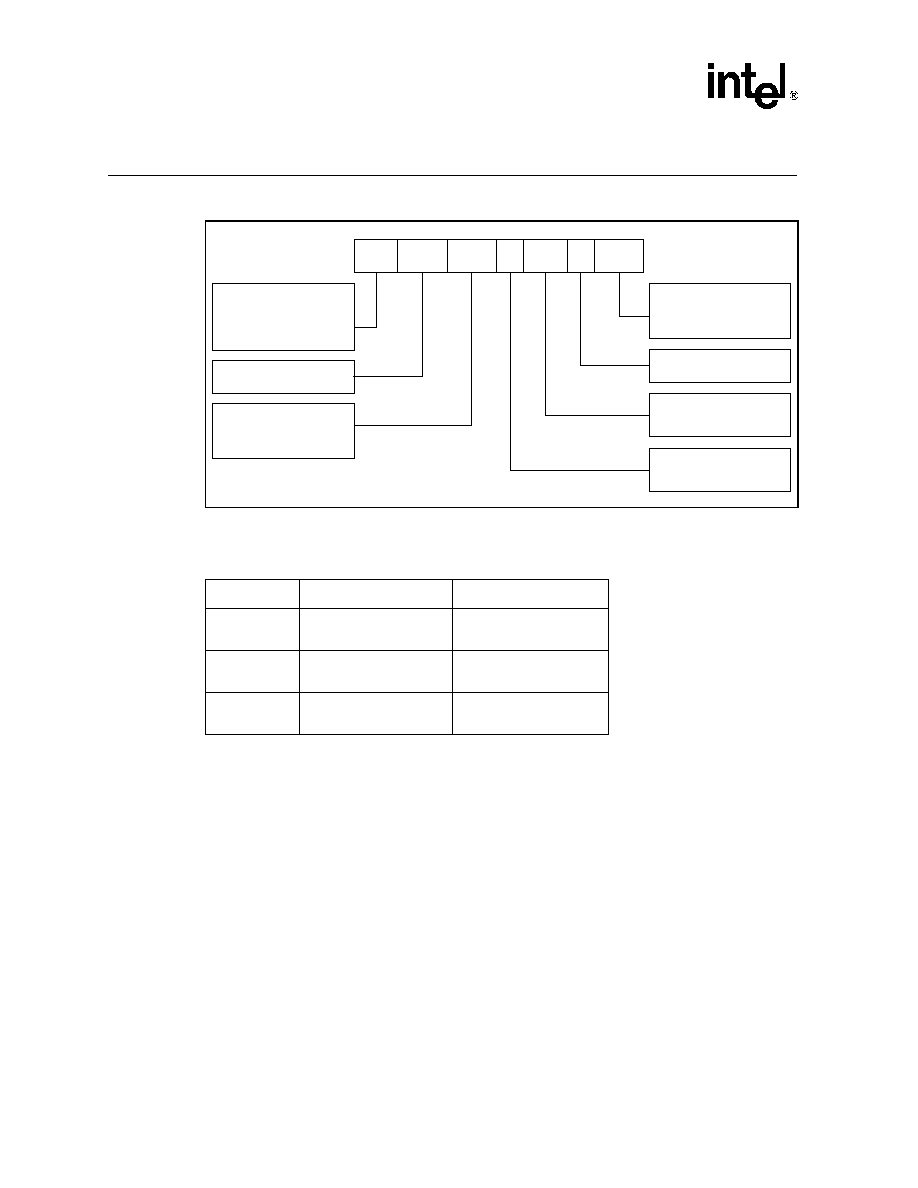
28F640K3, 28F640K18, 28F128K3, 28F128K18, 28F256K3, 28F256K18
78
Datasheet
Appendix F Order Information
RC 28F 128 K
Package Designator,
Extended Temperature
(-40C to +85C)
GE = 0.75 mm VF BGA
RC = Easy BGA
Product line designator
for all Intel
Æ
Flash products
Access Speed (ns)
64 Mbit = 110
128 Mbit = 115
256 Mbit = 120
Product Family
K = 3 Volt Synchronous Intel
StrataFlash
Æ
Memory
Process Identifier
C = 0.18um
115
Density
640 = 64 Mbit (8-MB x16)
128 = 128 Mbit (16-MB x16)
256 = 256 Mbit (32-MB x16)
18 C
Voltage Identifer (V
CC
/ V
CCQ
)
3 = 2.7 - 3.6V / 2.375 - 3.6V
18 = 2.7 - 3.6V / 1.65-1.95V
Table 33. Valid Combinations
Density
VF BGA
Easy BGA
64 Mbit
GE28F640K3C110
GE28F640K18C110
RC28F640K3C110
RC28F640K18C110
128 Mbit
GE28F128K3C115
GE28F128K18C115
RC28F128K3C115
RC28F128K18C115
256 Mbit
GE28F256K3C120
GE28F256K18C120
RC28F256K3C120
RC28F256K18C120