 | –≠–ª–µ–∫—Ç—Ä–æ–Ω–Ω—ã–π –∫–æ–º–ø–æ–Ω–µ–Ω—Ç: 386CXSA | –°–∫–∞—á–∞—Ç—å:  PDF PDF  ZIP ZIP |

Information in this document is provided solely to enable use of Intel products. Intel assumes no liability whatsoever, including infringe-
ment of any patent or copyright, for sale and use of Intel products except as provided in Intel's Terms and Conditions of Sale for such
products. Information contained herein supersedes previously published specifications on these devices from Intel.
© INTEL CORPORATION, 1994
September 1994
Order Number: 272418-003
Intel386TM CXSA
EMBEDDED MICROPROCESSOR
n
Static Intel386TM CPU Core
-- Low Power Consumption
-- Operating Power Supply
4.5V to 5.5V - 25 and 33 MHz
4.75V to 5.25V - 40 MHz
-- Operating Frequency
SA-40 = 40 MHz
SA-33 = 33 MHz
SA-25 = 25 MHz
n
Transparent Power-management System
Architecture
-- Intel System Management Mode
Architecture Extension for Truly
Compatible Systems
-- Power Management Transparent to
Operating Systems and Application
Programs
-- Programmable Power-management
Modes
n
Clock Freeze Mode Allows Clock
Stopping at Any Time
n
Full 32-bit Internal Architecture
-- 8-, 16-, 32-bit Data Types
-- 8 General Purpose 32-bit Registers
n
Runs Intel386 Architecture Software in a
Cost-effective, 16-bit Hardware
Environment
-- Runs Same Applications and
Operating Systems as the Intel386 SX
and Intel386 DX Processors
-- Object Code Compatible with 8086,
80186, 80286, and Intel386 Processors
n
High-performance 16-bit Data Bus
-- Two-clock Bus Cycles
-- Address Pipelining Allows Use of
Slower, Inexpensive Memories
n
Integrated Memory Management Unit
(MMU)
-- Virtual Memory Support
-- Optional On-chip Paging
-- 4 Levels of Hardware-enforced
Protection
-- MMU Fully Compatible with Those of
the 80286 and Intel386 DX Processors
n
Virtual 8086 Mode Allows Execution of
8086 Software in a Protected and Paged
System
n
Large, Uniform Address Space
-- 64 Megabyte Physical
-- 64 Terabyte Virtual
-- 4 Gigabyte Maximum Segment Size
n
Numerics Support with Intel387TM SX
and Intel387 SL Math Coprocessors
n
On-chip Debugging Support Including
Breakpoint Registers
n
Complete System Development Support
n
High-speed CHMOS Technology
n
100-pin Plastic Quad Flatpack Package
The Intel386TM CXSA embedded microprocessor is a 5-volt, 32-bit, fully static CPU with a 16-bit external data
bus, a 26-bit external address bus, and Intel's System Management Mode (SMM). The Intel386 CXSA CPU
brings the vast software library of the Intel386 architecture to embedded systems. It provides the performance
benefits of 32-bit programming with the cost savings associated with 16-bit hardware systems.
The Intel386 CXSA microprocessor is manufactured on Intel's 0.8-micron CHMOS V process. This process
provides high performance and low power consumption for power-sensitive applications. Figure 3 and Figure
4 illustrate the flexibility of low power devices with respect to temperature and frequency relationships.

Intel386TM CXSA EMBEDDED MICROPROCESSOR
2
Figure 1. Intel386TM CXSA Microprocessor Block Diagram
Decode
and
Sequencing
Control
ROM
Status
Flags
ALU
ALU
Control
Control
Prefetcher/
Limit
Checker
16-Byte
Code
Queue
Code
Stream
32
Segmentation Unit
Paging Unit
Bus Control
32
32
32
32
27
HOLD,
RESET
INTR, NMI
ERROR#
BUSY#,HLDA
SMI#, SMIACT#
BLE#, BHE#
A25:1, A20M#
M/IO#, D/C#
W/R#, LOCK#
ADS#, NA#
READY#
D15:0
Instruction
Prefetch
Control
Physical Address Bus
Adder
Page Cache
Control and
Attribute
PLA
Instruction
Decoder
3-Decoded
Instruction
Queue
Instruction
Predecode
MUX/
Trans-
ceivers
Pipeline/
Bus Size
Control
Address
Driver
Request
Prioritizer
3-Input
Adder
Descriptor
Register
Limit and
Attribute
PLA
Linear Address Bus
Displacement Bus
Barrel
Shifter/
Adder
Multiply/
Divide
Register
File
Protection
Test Unit
A2208-01
Internal Control Bus
32
Code Fetch/Page Table Fetch
Effective Address Bus
Effective Address Bus
Dedicated ALU Bus
Intel386TM CXSA EMBEDDED MICROPROCESSOR
3
1.0
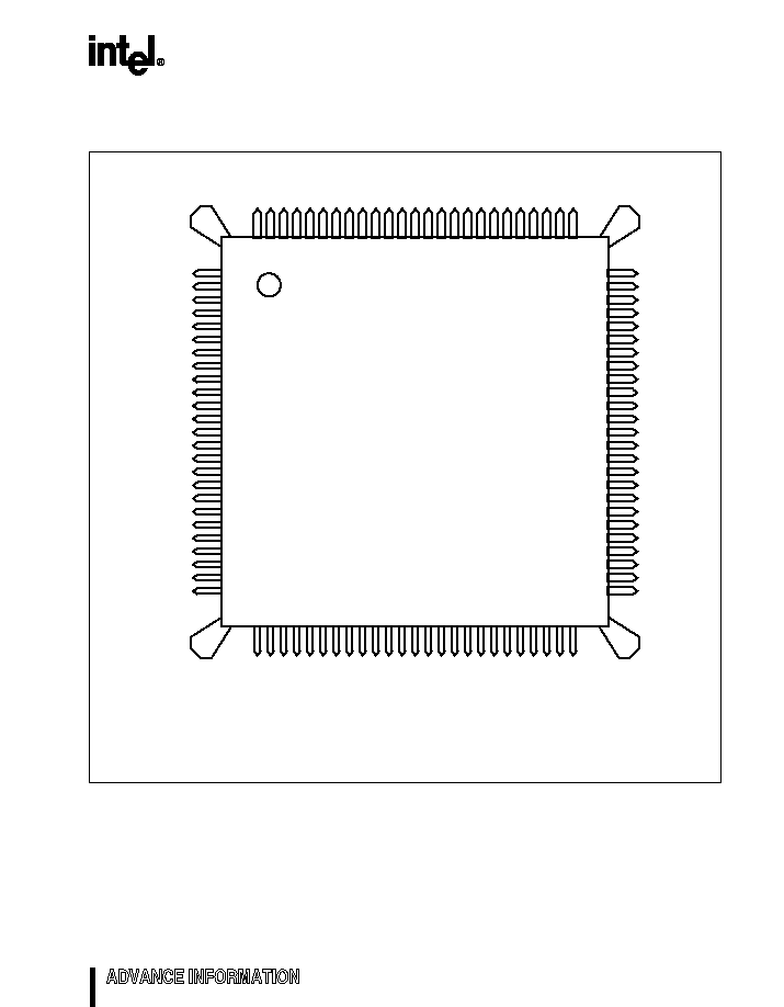
PIN ASSIGNMENT
Figure 2. Intel386TM CXSA Microprocessor Pin Assignment (PQFP)
NOTE:
NC = No Connection
1
2
3
4
5
6
7
8
9
10
11
12
13
14
15
16
17
18
19
20
21
22
23
24
25
75
74
73
72
71
70
69
68
67
66
65
64
63
62
61
60
59
58
57
56
55
54
53
52
51
A20
A19
A18
A17
Vcc
A16
Vcc
Vss
Vss
A15
A14
A13
Vss
A12
A11
A10
A9
A8
Vcc
A7
A6
A5
A4
A3
A2
100
99
98
97
96
95
94
93
92
91
90
89
88
87
86
85
84
83
82
81
80
79
78
77
76
26
27
28
29
30
31
32
33
34
35
36
37
38
39
40
41
42
43
44
45
46
47
48
49
50
D0
Vss
HLDA
HOLD
Vss
NA#
READY#
Vcc
Vcc
Vcc
Vss
Vss
Vss
Vss
CLK2
ADS#
BLE#
A1
BHE#
NC
Vcc
Vss
M/IO#
D/C#
W/R#
D1
D2
Vss
Vcc
D3
D4
D5
D6
D7
Vcc
D8
D9
D10
D11
D12
Vss
Vcc
D13
D14
D15
A23
A22
Vss
Vss
A21
LOCK#
NC
FLT#
NC
NC
NC
Vcc
RESET
BUSY#
Vss
ERROR#
PEREQ
NMI
Vcc
INTR
Vss
Vcc
SMIACT#
SMI#
A20M#
A24
A25
Vcc
Vss
Vss
TOP VIEW
A2207-01

Intel386TM CXSA EMBEDDED MICROPROCESSOR
4
Table 1. Pin Assignment
Pin
Symbol
Pin
Symbol
Pin
Symbol
Pin
Symbol
1
D0
26
LOCK#
51
A2
76
A21
2
V
SS
27
NC
52
A3
77
V
SS
3
HLDA
28
FLT#
53
A4
78
V
SS
4
HOLD
29
NC
54
A5
79
A22
5
V
SS
30
NC
55
A6
80
A23
6
NA#
31
NC
56
A7
81
D15
7
READY#
32
V
CC
57
V
CC
82
D14
8
V
CC
33
RESET
58
A8
83
D13
9
V
CC
34
BUSY#
59
A9
84
V
CC
10
V
CC
35
V
SS
60
A10
85
V
SS
11
V
SS
36
ERROR#
61
A11
86
D12
12
V
SS
37
PEREQ
62
A12
87
D11
13
V
SS
38
NMI
63
V
SS
88
D10
14
V
SS
39
V
CC
64
A13
89
D9
15
CLK2
40
INTR
65
A14
90
D8
16
ADS#
41
V
SS
66
A15
91
V
CC
17
BLE#
42
V
CC
67
V
SS
92
D7
18
A1
43
SMIACT#
68
V
SS
93
D6
19
BHE#
44
SMI#
69
V
CC
94
D5
20
NC
45
A20M#
70
A16
95
D4
21
V
CC
46
A24
71
V
CC
96
D3
22
V
SS
47
A25
72
A17
97
V
CC
23
M/IO#
48
V
CC
73
A18
98
V
SS
24
D/C#
49
V
SS
74
A19
99
D2
25
W/R#
50
V
SS
75
A20
100
D1

Intel386TM CXSA EMBEDDED MICROPROCESSOR
5
2.0
PIN DESCRIPTIONS
Table 2 lists the Intel386 CXSA microprocessor pin descriptions. The following definitions are used in the pin
descriptions:
#
The named signal is active low.
I
Input signal.
O
Output signal.
I/O Input and output signal.
P
Power pin.
G
Ground pin.
Table 2. Pin Descriptions
Symbol
Type
Pin
Name and Function
A20M#
(Note 1)
I
45
Address 20 Mask controls the A20 address signal. When
A20M# is low, the CPU masks off (forces low) the internal A20
physical address signal. This enables the CPU to run software
that was developed using the 8086 address "wraparound"
techniques. When A20M# is high, A20 is available on the
address bus. While the bus is floating, A20M# has no effect
on the A20 address signal. A20M# should be deasserted dur-
ing SMM if the SMM handler accesses more than 1 Mbyte of
memory.
A25:1
(Note 2)
O
47≠46, 80≠79,
76≠72, 70, 66-
64, 62≠58,
56≠51, 18
Address Bus outputs physical memory or port I/O addresses.
ADS#
O
16
Address Status indicates that the processor is driving a valid
bus-cycle definition and address onto its pins (W/R#, D/C#,
M/IO#, BHE#, BLE#, and A25:1).
BHE# O
19
Byte High Enable indicates that the processor is transferring
a high data byte.
BLE#
O
17
Byte Low Enable indicates that the processor is transferring
a low data byte.
BUSY#
I
34
Busy indicates that the math coprocessor is busy.
CLK2
I
15
CLK2 provides the fundamental timing for the device.
D/C#
O
24
Data/Control indicates whether the current bus cycle is a
data cycle (memory or I/O) or a control cycle (interrupt
acknowledge, halt, or code fetch). When D/C# is high, the bus
cycle is a data cycle; when D/C# is low, the bus cycle is a con-
trol cycle.
D15:0
I/O
81≠83, 86≠90,
92≠96, 99≠100,
1
Data Bus inputs data during memory read, I/O read, and
interrupt acknowledge cycles and outputs data during mem-
ory and I/O write cycles.
NOTES:
1. This pin supports the additional features of the Intel386 CXSA microprocessor; it is not present on the Intel386 SXSA microprocessor.
2. The A25:24 pins support the additional features of the Intel386 CXSA microprocessor; they are not present on the Intel386 SXSA micro-
processor.

Intel386TM CXSA EMBEDDED MICROPROCESSOR
6
ERROR#
I
36
Error indicates that the math coprocessor has an error condi-
tion.
FLT#
I
28
Float forces all bidirectional and output signals, including
HLDA, to a high-impedance state.
HLDA
O
3
Bus Hold Acknowledge indicates that the CPU has surren-
dered control of its local bus to another bus master.
HOLD
I
4
Bus Hold Request allows another bus master to request con-
trol of the local bus.
INTR
I
40
Interrupt Request is a maskable input that causes the CPU
to suspend execution of the current program and then exe-
cute an interrupt acknowledge cycle.
LOCK#
O
26
Bus Lock prevents other system bus masters from gaining
control of the system bus while it is active (low).
M/IO#
O
23
Memory/IO indicates whether the current bus cycle is a mem-
ory cycle or an input/output cycle. When M/IO# is high, the
bus cycle is a memory cycle; when M/IO# is low, the bus cycle
is an I/O cycle.
NA#
I
6
Next Address requests address pipelining.
NC
20, 27, 29≠31
No Connection should always be left unconnected. Connect-
ing a NC pin may cause the processor to malfunction or cause
your application to be incompatible with future steppings of
the device.
NMI
I
38
Nonmaskable Interrupt Request is a nonmaskable input
that causes the CPU to suspend execution of the current pro-
gram and execute an interrupt acknowledge function.
PEREQ
I
37
Processor Extension Request indicates that the math
coprocessor has data to transfer to the processor.
READY#
I
7
Bus Ready indicates that the current bus cycle is finished and
the external device is ready to accept more data from the pro-
cessor.
RESET
I
33
Reset suspends any operation in progress and places the
processor into a known reset state.
Table 2. Pin Descriptions (Continued)
Symbol
Type
Pin
Name and Function
NOTES:
1. This pin supports the additional features of the Intel386 CXSA microprocessor; it is not present on the Intel386 SXSA microprocessor.
2. The A25:24 pins support the additional features of the Intel386 CXSA microprocessor; they are not present on the Intel386 SXSA micro-
processor.

Intel386TM CXSA EMBEDDED MICROPROCESSOR
7
SMI#
(Note 1)
I
44
System Management Interrupt invokes System Manage-
ment Mode (SMM). SMI# is the highest priority interrupt. It is
latched on its falling edge and it forces the CPU into SMM
upon completion of the current instruction. SMI# is recognized
on an instruction boundary and at each iteration for repeat
string instructions. SMI# cannot interrupt LOCKed bus cycles
or a currently executing SMM. If the processor receives a sec-
ond SMI# while it is in SMM, it will latch the second SMI# on
the SMI# falling edge. However, the processor must exit SMM
by executing a Resume instruction (RSM) before it can ser-
vice the second SMI#.
SMIACT#
(Note 1)
O 43
System Management Interrupt Active indicates that the
processor is operating in System Management Mode (SMM).
It is asserted when the processor initiates an SMM sequence
and remains asserted (low) until the processor executes the
Resume instruction (RSM).
W/R#
O
25
Write/Read indicates whether the current bus cycle is a write
cycle or a read cycle. When W/R# is high, the bus cycle is a
write cycle; when W/R# is low, it is a read cycle.
V
CC
P
8≠10, 21, 32,
39, 42, 48, 57,
69, 71, 84, 91,
97
System Power provides the nominal DC supply input.
V
SS
G
2, 5, 11≠14, 22
35, 41, 49≠50,
63, 67≠68,
77≠78, 85, 98
System Ground provides the 0V connection from which all
inputs and outputs are measured.
Table 2. Pin Descriptions (Continued)
Symbol
Type
Pin
Name and Function
NOTES:
1. This pin supports the additional features of the Intel386 CXSA microprocessor; it is not present on the Intel386 SXSA microprocessor.
2. The A25:24 pins support the additional features of the Intel386 CXSA microprocessor; they are not present on the Intel386 SXSA micro-
processor.
Intel386TM CXSA EMBEDDED MICROPROCESSOR
8
3.0
DESIGN CONSIDERATIONS
This section describes the Intel386 CXSA micropro-
cessor instruction set, component and revision
identifier, and package thermal specifications.
3.1.
Instruction Set
The Intel386 CXSA microprocessor uses the same
instruction set as the Intel386 SX microprocessor
with the following exceptions.
The Intel386 CXSA microprocessor has one new
instruction (RSM). This Resume instruction causes
the processor to exit System Management Mode
(SMM). RSM requires 338 clocks for execution.
The Intel386 CXSA microprocessor requires more
clock cycles than the Intel386 SX microprocessor to
execute some instructions. Table 4 lists these
instructions and the Intel386 CXSA microprocessor
execution times. For the equivalent Intel386 SX
microprocessor execution times, refer to the
"Instruction Set Clock Count Summary" table in the
Intel386TM SX Microprocessor
data sheet (order
number 240187).
3.2.
Component and Revision
Identifier
To assist users, the microprocessor holds a
component identifier and revision identifier in its DX
register after reset. The upper 8 bits of DX hold the
component identifier, 23H. (The lower nibble, 3H,
identifies the Intel386 architecture, while the upper
nibble, 2H, identifies the second member of the
Intel386 microprocessor family.)
The lower 8 bits of DX hold the revision level
identifier. The revision identifier will, in general,
chronologically track those component steppings
that are intended to have certain improvements or
distinction from previous steppings. The revision
identifier will track that of the Intel386 CPU
whenever possible. However, the revision identifier
value is not guaranteed to change with every
stepping revision or to follow a completely uniform
numerical sequence, depending on the type or
intent of the revision or the manufacturing materials
required to be changed. Intel has sole discretion
over these characteristics of the component. The
initial revision identifier for the Intel386 CXSA
microprocessor is 09H.
3.3.
Package Thermal Specifications
The Intel386 CXSA microprocessor is specified for
operation with case temperature (T
CASE
) as
specified in the "DC SPECIFICATIONS" on
page 10. The case temperature can be measured
in any environment to determine whether the micro-
processor is within the specified operating range.
The case temperature should be measured at the
center of the top surface opposite the pins.
An increase in the ambient temperature (T
A
) causes
a proportional increase in the case temperature
(T
CASE
) and the junction temperature (T
J
). See
Figures 3 and Figures 4 for case and ambient
temperature relationships to frequency. A packaged
device produces thermal resistance between
junction and case temperatures (
JC
) and between
junction and ambient temperatures (
JA
). The
relationships between the temperature and thermal
resistance parameters are expressed by these
equations (P = power dissipated as heat = V
CC
◊
I
CC
):
1.
T
J
= T
CASE
+ P
◊
JC
2.
T
A
= T
J
≠ P
◊
JA
3.
T
CASE
= T
A
+ P
◊
[
JA
≠
JC
]
A safe operating temperature can be calculated
from equation 1 by using the maximum safe T
J
of
115∞ C, the maximum power drawn by the chip in
the specific design, and the
JC
value from Table 3.
The
J
A
value depends on the airflow (measured at
the top of the chip) provided by the system venti-
lation. The
J
A
values are given for reference only
and are not guaranteed.
Table 3. Thermal Resistances (0∞C/W)
JA
,
JC
Pkg
JC
JA
versus Airflow (ft/min)
0
100
200
100 PQFP
5.1
46.0
44.8
41.2

Intel386TM CXSA EMBEDDED MICROPROCESSOR
9
Table 4. Intel386TM CXSA Microprocessor Instruction Execution Times (in Clock Counts)
Instruction
Clock Count
Virtual 8086 Mode
(Note 1)
Real Address Mode
or Virtual 8086 Mode
Protected Virtual
Address Mode
(Note 3)
POPA
28
35
IN:
Fixed Port
Variable Port
27
28
14
15
7/29
8/29
OUT:
Fixed Port
Variable Port
27
28
14
15
7/29
9/29
INS
30
17
9/32
OUTS
31
18
10/33
REP INS
31+6n (Note 2)
17+6n (Note 2)
10+6n/32+6n (Note 2)
REP OUTS
30+8n (Note 2)
16+8n (Note 2)
10+8n/31+8n (Note 2)
HLT
7
7
MOV C0, reg
10
10
NOTES:
1. The clock count values in this column apply if I/O permission allows I/O to the port in virtual 8086 mode. If the I/O bit map denies permission,
exception fault 13 occurs; see clock counts for the INT 3 instruction in the "Instruction Set Clock Count Summary" table in the
Intel386TM SX
Microprocessor data sheet (order number 240187).
2. n = the number of times repeated.
3. When two clock counts are listed, the smaller value refers to a register operand and the larger value refers to a memory operand.
Intel386TM CXSA EMBEDDED MICROPROCESSOR
10
4.0
DC SPECIFICATIONS
ABSOLUTE MAXIMUM RATINGS*
Storage Temperature ................................. ≠65∞C to +150∞C
Case Temperature Under Bias .................. ≠65∞C to +112∞C
Supply Voltage with Respect to
V
SS
............... ≠0.5V to 6.5V
Voltage on Other Pins .......................... ≠0.5V to
V
CC
+ 0.5V
OPERATING CONDITIONS*
V
CC
(Digital Supply Voltage - 25 and 33 MHz) ... 4.5V to 5.5V
V
CC
(Digital Supply Voltage - 40 MHz) ........... 4.75V to 5.25V
T
CASE
minimum (Case Temperature Under Bias)
.........
0∞C
T
CASE
maximum
..........................................
see Figure 4
Operating Frequency ................................ 0 MHz to 40 MHz
NOTICE: This document contains information on
products in the sampling and initial production
phases of development. The specifications are sub-
ject to change without notice. Verify with your local
Intel Sales office that you have the latest data sheet
before finalizing a design.
*WARNING: Stressing the device beyond the "Absolute
Maximum Ratings" may cause permanent damage. These
are stress ratings only. Operation beyond the "Operating
Conditions" is not recommended and extended exposure
beyond the "Operating Conditions" may affect device
reliability.
Table 5. DC Characteristics
Symbol
Parameter
Min.
Max.
Unit
Test Condition
V
IL
Input
Low
Voltage
≠0.3
+0.8
V
V
IH
Input
High
Voltage
2.0
V
CC
+ 0.3
V
V
ILC
CLK2
Input
Low
Voltage
≠0.3
+0.8
V
V
IHC
CLK2 Input High Voltage
V
CC
≠ 0.8
V
CC
+ 0.3
V
V
OL
Output Low Voltage
0.45
V
I
OL
= 5 mA
V
OH
Output
High
Voltage
2.4
V
CC
≠ 0.5
V
V
I
OH
= ≠1 mA
I
OH
= ≠0.2 mA
I
LI
Input
Leakage
Current
(for all pins except PEREQ,
BUSY#, FLT#, ERROR#,
A20M#, SMI#)
±15
µA
0
V
IN
V
CC
I
IH
Input
Leakage
Current
(PEREQ)
150
µA
V
IH
= 2.4V (Note 1)
I
IL
Input
Leakage
Current
(BUSY#, FLT#, ERROR#,
A20M#, and SMI#)
≠120
µA
V
IL
= 0.45V (Note 2)
I
LO
Output Leakage Current
±15
µA
0.45V
V
OUT
V
CC
I
CC
Supply
Current
CLK2 = 80 MHz, CLK = 40
MHz
CLK2 = 66 MHz, CLK = 33
MHz
CLK2 = 50 MHz, CLK = 25
MHz
275
225
175
mA
mA
mA
(Notes 3, 4)
typical = 200 mA
typical = 175 mA
typical = 140 mA
I
CCF
Standby Current (Freeze Mode)
150
µA
typical = 10 µA (Notes 3, 4)
C
IN
Input
Capacitance
10
pF
F
C
= 1 MHz (Note 5)
NOTES:
1. PEREQ input has an internal weak pull-down resistor.
2. BUSY#, FLT#, SMI#, A20M# and ERROR# inputs each have an internal weak pull-up resistor.
3. I
CC
max measurement at worst-case frequency, V
CC
, and temperature with reset active.
4. I
CC
typical and I
CCF
typical are measured at nominal V
CC
and are not fully tested.
5. Not fully tested.

Intel386TM CXSA EMBEDDED MICROPROCESSOR
11
Figure 3. Ambient Temperature vs. Frequency at Zero Air Flow and T
J
= 115∞ C
C
OUT
Output or I/O Capacitance
12
pF
F
C
= 1 MHz (Note 5)
C
CLK
CLK2
Capacitance
20
pF
F
C
= 1 MHz (Note 5)
Table 5. DC Characteristics (Continued)
Symbol
Parameter
Min.
Max.
Unit
Test Condition
NOTES:
1. PEREQ input has an internal weak pull-down resistor.
2. BUSY#, FLT#, SMI#, A20M# and ERROR# inputs each have an internal weak pull-up resistor.
3. I
CC
max measurement at worst-case frequency, V
CC
, and temperature with reset active.
4. I
CC
typical and I
CCF
typical are measured at nominal V
CC
and are not fully tested.
5. Not fully tested.
A2586-01
100
75
50
25
T (∞C)
a
Operating Frequency (MHz)
12
16
20
25
33
40
90
85
80
70
58
45

Intel386TM CXSA EMBEDDED MICROPROCESSOR
12
Figure 4. Case Temperature vs. Frequency at T
J
= 115∞ C
A2587-01
115
105
T (∞C)
c
Operating Frequency (MHz)
12
16
20
25
33
40
110
112
111.5
111
110
108.5
107

Intel386TM CXSA EMBEDDED MICROPROCESSOR
13
5.0
AC SPECIFICATIONS
Table 6 lists output delays, input setup require-
ments, and input hold requirements. All AC specifi-
cations are relative to the CLK2 rising edge
crossing the 2.0V level.
Figure 5 shows the measurement points for AC
specifications. Inputs must be driven to the
indicated voltage levels when AC specifications are
measured. Output delays are specified with
minimum and maximum limits measured as shown.
The minimum delay times are hold times provided
to external circuitry. Input setup and hold times are
specified as minimums, defining the smallest
acceptable sampling window. Within the sampling
window, a synchronous input signal must be stable
for correct operation.
Outputs ADS#, W/R#, D/C#, MI/O#, LOCK#, BHE#,
BLE#, A25:1, SMIACT# and HLDA change only at
the beginning of phase one. D15:0 (write cycles)
change only at the beginning of phase two.
The READY#, HOLD, BUSY#, ERROR#, PEREQ,
FLT#, A20M# and D15:0 (read cycles) inputs are
sampled at the beginning of phase one. The NA#,
INTR, SMI# and NMI inputs are sampled at the
beginning of phase two.

Intel386TM CXSA EMBEDDED MICROPROCESSOR
14
Figure 5. Drive Levels and Measurement Points for AC Specifications
A
B
Tx
Valid
Output n+1
a
a
a
a
b
Min
Max
C
D
CLK2
OUTPUTS
(A25:1,BHE#
BLE#,ADS#,M/IO#
D/C#W/R#,LOCK#
HLDA, SMIACT#)
OUTPUTS
(D15:0)
INPUTS
(N/A#,INTR
NMI,SMI#)
INPUTS
(READY#,HOLD
FLT#,ERROR#
BUSY#,PEREQ
D15:0,A20M#)
LEGEND
a - 1.5V
b - 2.0V
A - Maximum Output Delay Spec
B - Minimum Output Delay Spec
C - Minimum Input Setup Spec
D - Minimum Input Hold Spec
PH1
PH2
3.0V
0V
Valid
Output n
A
B
Valid
Output n+1
a
a
Min
Max
Valid
Output n
Valid
Input
a
a
C
D
3.0V
0V
Valid
Input
A2206-02

Intel386TM CXSA EMBEDDED MICROPROCESSOR
15
Table 6. AC Characteristics
Symbol
Parameter
40 MHz
33 MHz
25 MHz
Test Condition
Min.
(ns)
Max.
(ns)
Min.
(ns)
Max.
(ns)
Min.
(ns)
Max.
(ns)
Operating Frequency
0
40
0
33
0
25
MHz (Note 1)
t1
CLK2 Period
12.5
15
20
t2a
CLK2 High Time
4.5
6.25
7
(Note 2)
t2b
CLK2 High Time
3.5
4
4
(Note 2)
t3a
CLK2 Low Time
4.5
6.25
7
(Note 2)
t3b
CLK2 Low Time
3.5
4.5
5
(Note 2)
t4
CLK2 Fall Time
4
4
7
(Note 2)
t5
CLK2 Rise Time
4
4
7
(Note 2)
t6
A25:1 Valid Delay
4
13
4
15
4
17
C
L
= 50 pF
t7
A25:1 Float Delay
4
20
4
20
4
30
(Note 3)
t8
BHE#, BLE#, LOCK#
Valid Delay
4
13
4
15
4
17
C
L
= 50 pF
t8a
SMIACT# Valid
Delay
4
13
4
15
4
17
C
L
= 50 pF
t9
BHE#, BLE#, LOCK#
Float Delay
4
20
4
20
4
30
(Note 3)
t10
W/R#, M/IO#, D/C#,
ADS# Valid Delay
4
13
4
15
4
17
C
L
= 50 pF
t11
W/R#, M/IO#, D/C#,
ADS# Float Delay
4
20
4
20
4
30
(Note 3)
t12
D15:0 Write Data
Valid Delay
7
18
7
23
7
23
C
L
= 50 pF
(Note 5)
t12a
D15:0 Write Data
Hold Time
2
2
2
C
L
= 50 pF
t13
D15:0 Write Data
Float delay
4
17
4
17
4
22
(Note 3)
t14
HLDA Valid Delay
4
17
4
20
4
22
C
L
= 50 pF
t15
NA# Setup Time
5
5
5
t16
NA# Hold Time
2
2
3
t19
READY#, A20M#
Setup Time
7
7
9
NOTES:
1. Tested at maximum operating frequency and guaranteed by design characterization at lower operating frequencies.
2. These are not tested. They are guaranteed by characterization.
3. Float condition occurs when maximum output current becomes less than I
LO
in magnitude. Float delay is not fully tested.
4. These inputs may be asynchronous to CLK2. The setup and hold specifications are given for testing purposes to ensure recognition within
a specific CLK2 period.
5. Minimum time not 100% tested.

Intel386TM CXSA EMBEDDED MICROPROCESSOR
16
t20
READY#, A20M#
Hold Time
4
4
4
t21
D15:0 Read Setup
Time
4
5
7
t22
D15:0 Read Hold
Time
3
3
5
t23
HOLD Setup Time
4
9
9
t24
HOLD Hold Time
2
2
3
t25
RESET Setup Time
4
5
8
t26
RESET Hold Time
2
2
3
t27
NMI, INTR Setup
Time
5
5
6
(Note 4)
t27a
SMI# Setup Time
5
5
6
(Note 4)
t28
NMI, INTR Hold
Time
5
5
6
(Note 4)
t28a
SMI# Hold Time
5
5
6
(Note 4)
t29
PEREQ, ERROR#,
BUSY#, FLT# Setup
Time
5
5
6
(Note 4)
t30
PEREQ, ERROR#,
BUSY#, FLT# Hold
Time
4
4
5
(Note 4)
Table 6. AC Characteristics (Continued)
Symbol
Parameter
40 MHz
33 MHz
25 MHz
Test Condition
Min.
(ns)
Max.
(ns)
Min.
(ns)
Max.
(ns)
Min.
(ns)
Max.
(ns)
NOTES:
1. Tested at maximum operating frequency and guaranteed by design characterization at lower operating frequencies.
2. These are not tested. They are guaranteed by characterization.
3. Float condition occurs when maximum output current becomes less than I
LO
in magnitude. Float delay is not fully tested.
4. These inputs may be asynchronous to CLK2. The setup and hold specifications are given for testing purposes to ensure recognition within
a specific CLK2 period.
5. Minimum time not 100% tested.

Intel386TM CXSA EMBEDDED MICROPROCESSOR
17
Figure 6. AC Test Loads
Figure 7. CLK2 Waveform
A2200-0A
CPU Output
C
L
CLK2
t
4
A
B
C
A = Vcc ≠ 0.8
B = 2.0V
C = 0.8V
t
3b
t
3a
t
1
t
2a
t
2b
t
5
A2201-01

Intel386TM CXSA EMBEDDED MICROPROCESSOR
18
Figure 8. AC Timing Waveforms -- Input Setup and Hold Timing
A2202-01
CLK2
TX
TX
TX
READY#
A20M#
HOLD
D15:0
(Input)
BUSY#
ERROR#
PEREQ
FLT#
NA#
INTR
NMI
SMI#
PH2
PH1
PH2
PH1
t19
t20
t23
t24
t21
t22
t29
t30
t15
t16
t27
t28
t27a
t28a

Intel386TM CXSA EMBEDDED MICROPROCESSOR
19
Figure 9. AC Timing Waveforms -- Output Valid Delay Timing
CLK2
TX
TX
TX
BHE#, BLE#
LOCK#
SMIACT#
W/R#, M/IO#
D/C#, ADS#
A25:1
D15:0
(Output)
PH2
PH1
PH2
PH1
Min
Valid n+1
Valid n
Max
Min
Valid n+1
Valid n
Max
Min
Valid n+1
Valid n
Max
Min
Valid n+1
Max
Valid n
HLDA
t8, t8a
t10
t6
t12,t12a
A2203-01

Intel386TM CXSA EMBEDDED MICROPROCESSOR
20
Figure 10. AC Timing Waveforms -- Output Float Delay and HLDA Valid Delay Timing
CLK2
TI or T1
BHE#, BLE#
LOCK#
W/R#, M/IO#
D/C#, ADS#
A25:1
D15:0
PH2
PH1
PH2
PH1
Min
Max
HLDA
PH2
Th
Min
Max
(High Z)
Min
Max
Min
Max
(High Z)
Min
Max
Min
Max
(High Z)
Min
Max
Min
Max
(High Z)
t13 Also applies to data float when write
cycle is followed by read or idle.
Min
Max
Min
Max
t8
t10
t6
t11
t7
t9
t13
t14
t14
t12
A2204-01

Intel386TM CXSA EMBEDDED MICROPROCESSOR
21
Figure 11. AC Timing Waveforms -- RESET Setup and Hold Timing and Internal Phase
6.0
REVISION HISTORY
This -003 data sheet contains the following changes from the -002 version.
∑ Changed V
CC
at 40 MHz to 4.75V to 5.25V (pages 1 and 10).
∑ Renamed "Powerdown Mode" to "Clock Freeze Mode" on page 1.
∑ Added clarifications to Figure 1.
∑ Corrected pin numbering for A25:1 in Table 2.
∑ Changed first sentence in Section 3.3 from "...on page 12" to "...on page 10."
∑ Changed note 2 on page 10 to reflect A20M#
∑ Changed first sentence on page 13 from "Table 7 lists..." to "Table 6 lists..."
∑ Added INTR and A20M# to Figure 8 and removed BS8#.
CLK2
RESET
PH2
PH1
PH2 or PH1
PH2 or PH1
Reset
Initialization Sequence
t26
t25
A2205-0A