 | –≠–ª–µ–∫—Ç—Ä–æ–Ω–Ω—ã–π –∫–æ–º–ø–æ–Ω–µ–Ω—Ç: 440MX-100 | –°–∫–∞—á–∞—Ç—å:  PDF PDF  ZIP ZIP |

Order Number- 245292-001
82443MX100 PCIset
Datasheet
ß
Processor Host Bus Support
Optimized for the IntelÆ mobile
PentiumÆ II and the mobile
CeleronTM processors at 100 MHz
or 66 MHz
GTL+ Bus Driver Technology
ß
Integrated DRAM Support
--
8 MB to 256 MB using 16-Mb,
64-Mb, and 128-Mb Technology
--
Standard and Registered
SDRAM (Synchronous) DRAM
Support (x-1-1-1 access at 100
MHz or 66 MHz)
Enhanced Open Page Arbitration
SDRAM Paging Scheme
ß
PCI Bus Interface
PCI Rev. 2.3, 3.3-V, 33-MHz
Interface Compliant
ß
Integrated IDE Controller
One Channel Support for "Ultra
DMA/33" Synchronous DMA
Mode
ß
System Peripheral Support
Enhanced DMA Controller
Support for Dual Cascaded
82C37 Controllers
Interrupt Controller based on two
82C59 for up to 15 Interrupts
System Timer based on 82C54
Real Time Clock with 256-Bytes
Battery backed RAM
ß
X-bus Support for SIO, KBCX, and
Flash
ß
USB
AC'97 Link Controller
ß
AC'97 Audio Modem CODEC
Interface Support
USB 1.1 Port for Serial Transfers
at 12 or 1.5 Mbits/sec
Supports UHCI Design Guide
ß
SMBus Support
ß
Power Management Logic
Support for Power-On-Suspend,
Suspend-To-SDRAM, and
Suspend-To-Disk
Support for Thermal Alarm
Full Support for ACPI
Specification Revision 1.0
ß
31 GPIO Pins
ß
Thermal Design Power
2.1W for 100 MHz
1.6W for 66 MHz
ß
492 uBGA Package
The Intel 82443MX100 PCIset integrates the traditional "North Bridge" and "South Bridge" into
one device, which reduces power and board space for Intel mobile Pentium II processor-based
designs and mobile Celeron processor-based designs.
The Intel 82443MX100 PCIset may contain design defects or errors know as errata,
which may cause the product to deviate from published specifications. Current
characterized errata are available upon request.

ii
Datasheet
Information in this document is provided in connection with Intel products. No license, express or implied, by estoppel or
otherwise, to any intellectual property rights is granted by this document. Except as provided in Intel's Terms and Conditions of
Sale for such products, Intel assumes no liability whatsoever, and Intel disclaims any express or implied warranty, relating to
sale and/or use of Intel products including liability or warranties relating to fitness for a particular purpose, merchantability, or
infringement of any patent, copyright or other intellectual property right. Intel products are not intended for use in medical, life
saving, or life sustaining applications.
Intel retains the right to make changes to specifications and product descriptions at any time, without notice.
The mobile CeleronTM processor, mobile PentiumÆ II processor, and 82443MX100 controller products may contain design
defects or errors known as errata which may cause the product to deviate from published specifications. Current characterized
errata are available on request.
The Intel 82443MX100 PCIset Datasheet is provided "AS IS" WITH NO WARRANTIES WHATSOEVER, INCLUDING ANY
WARRANTY OF MERCHANTABILITY, NONINFRINGEMENT, FITNESS FOR ANY PARTICULAR PURPOSE, OR ANY
WARRANTY OTHERWISE ARISING OUT OF ANY PROPOSAL, SPECIFICATION OR SAMPLE.
Intel disclaims all liability, including liability for infringement of any proprietary rights, relating to use of information in this
specification. No license, express or implied, by estoppel or otherwise, to any intellectual property rights is granted herein.
I2C is a two-wire communications bus/protocol developed by Philips. SMBus is a subset of the I2C bus/protocol and was
developed by Intel. Implementations of the I2C bus/protocol or the SMBus bus/protocol may require licenses from various
entities, including Philips Electronics N.V. and North American Philips Corporation.
Copies of documents which have an ordering number and are referenced in this document, or other Intel literature, may be
obtained from:
Intel Corporation
P.O. Box 7641
Mt. Prospect IL 60056-7641
or call 1-800-879-4683
*Other brands and names are the property of their respective owners.
Copyright © Intel Corporation, 1999.

Intel
Æ
82443MX100 PCIset
Datasheet
i
CONTENTS
1.0
Introduction .................................................................................................................. 1
1.1
References ........................................................................................................ 1
1.2
440MX Feature Summary .................................................................................. 2
1.3
440MX Features................................................................................................. 3
2.0
Architecture Overview.................................................................................................. 6
3.0
Signal Description and Pin States ............................................................................... 7
3.1
Pin List............................................................................................................... 7
3.1.1
Signal Description.................................................................................. 8
3.1.2
Power and Ground Pins....................................................................... 19
3.2
GPIO Definition ................................................................................................ 20
3.3
Power Rail Overview ........................................................................................ 22
3.4
Power-up State Initial Value ............................................................................. 23
3.5
Power-On-Reset Pin Values............................................................................. 24
3.6
Power-up/Reset Strap Options ......................................................................... 30
3.7
CPU Reset....................................................................................................... 31
4.0
Power Planes .............................................................................................................. 33
4.1
Overview.......................................................................................................... 33
4.2
RTC Power Plane ............................................................................................ 33
4.3
Resume Power Plane....................................................................................... 33
5.0
System Address Map.................................................................................................. 35
5.1
Addressable Memory Support .......................................................................... 35
5.2
Memory Map.................................................................................................... 35
5.2.1
Compatibility Area ............................................................................... 37
5.2.1.1
DOS Area (00000h-9FFFh; 0 - 640 KB) .............................. 38
5.2.1.2
Video Buffer Area (A0000h-BFFFFh; 640 - 768 KB)............ 38
5.2.1.3
Expansion Area (C0000h-DFFFFh; 768 - 896 KB) .............. 38
5.2.1.4
Extended System BIOS Area (E0000h-EFFFFh; 896 - 960
KB)..................................................................................... 38
5.2.1.5
System BIOS Area (F0000h-FFFFFh; 960 KB - 1 MB) ........ 38
5.2.2
Extended Memory Area ....................................................................... 39
5.2.2.1
Main DRAM Address Range (0010_0000h to Top of Main
Memory)............................................................................. 39
5.2.2.2
Extended SMRAM Address Range (Top of Main Memory -
TSEG_SZ to Top of Main Memory)..................................... 39
5.2.2.3
PCI Memory Address Range (Top of Main Memory to 4 GB) ..
.......................................................................................... 39
5.2.2.4
High BIOS Area (FFC0_0000h - FFFF_FFFFh) .................. 39
5.3
System Management Mode (SMM) Memory Range.......................................... 40
5.4
Memory Shadowing.......................................................................................... 40
5.5
Decode Rules and Cross-Bridge Address Mapping .......................................... 40
5.5.1
PCI Interface Memory Decode Rules ................................................... 40
5.5.2
Legacy VGA Range ............................................................................. 40
5.6
I/O Address Space ........................................................................................... 41

Intel
Æ
82443MX100 PCIset
ii
Datasheet
5.6.1
Fixed I/O Address Ranges ................................................................... 41
5.6.2
Variable I/O Decode Ranges................................................................ 45
6.0
Functional Description ............................................................................................... 48
6.1
Mobile Celeron Processor and Mobile Pentium
II
Processor Host Interface ...... 48
6.1.1
Overview ............................................................................................. 48
6.1.2
Host Bus Device Support..................................................................... 48
6.1.3
Special Cycles ..................................................................................... 49
6.1.4
Symmetric Multiprocessor (SMP) Configuration ................................... 50
6.1.5
In-order Queue Pipelining .................................................................... 50
6.1.6
Frame Buffer Memory Support (USWC)............................................... 50
6.1.7
CPU Sideband Interface ...................................................................... 51
6.1.7.1
A20M#................................................................................ 51
6.1.7.2
FERR#/IGNNE# (Co-processor Error) ................................ 51
6.1.7.3
INIT# .................................................................................. 52
6.1.7.4
Interrupt Signals ................................................................. 52
6.1.7.5
NMI .................................................................................... 52
6.1.7.6
SMI# .................................................................................. 52
6.1.7.7
STPCLK# ........................................................................... 53
6.2
Memory Interface ............................................................................................. 53
6.2.1
DRAM Interface ................................................................................... 53
6.2.1.1
DRAM Interface Overview .................................................. 53
6.2.2
DRAM Organization and Configuration ................................................ 53
6.2.2.1
Configuration Mechanism for DIMMs .................................. 55
6.2.2.1.1
Memory Detection and Initialization.................. 55
6.2.2.1.2
SMBus Configuration ....................................... 56
6.2.2.1.3
Accessing the Serial Presence Detect Ports..... 56
6.2.2.1.4
DRAM Register Programming.......................... 56
6.2.3
SDRAM Cycle Encoding ...................................................................... 57
6.2.4
DRAM Address Translation and Decoding ........................................... 62
6.2.5
SDRAMC Register Programming ......................................................... 63
6.2.6
SDRAM Paging Policy ......................................................................... 64
6.2.6.1
Overview ............................................................................ 64
6.2.6.2
Open Page Arbitration Policies ........................................... 64
6.2.6.3
Selective Auto Precharge Policy ......................................... 64
6.2.7
DRAM Power Throttling ....................................................................... 64
6.2.7.1
Overview ............................................................................ 64
6.2.7.2
Conceptual Description of Power Throttling......................... 64
6.2.7.2.1
During Monitoring Regime ............................... 64
6.2.7.2.2
During Throttling Regime ................................. 65
6.2.7.2.3
Read and Write Throttling Regimes.................. 65
6.2.7.2.4
The Relation Between Read and Write Throttling .
........................................................................ 66
6.2.7.3
SDRAM Power Throttling Setting Sequence ....................... 66
6.2.8
SDRAM Performance Description ........................................................ 66
6.2.9
SDRAM Optimizations ......................................................................... 66
6.2.9.1
Dual and Quad Bank Support ............................................. 66
6.3
System Memory Management.......................................................................... 67
6.3.1
SMRAM Range Overview .................................................................... 67

Intel
Æ
82443MX100 PCIset
Datasheet
iii
6.3.2
Compatible SMRAM (C_SMRAM)........................................................ 67
6.3.3
Extended SMRAM (E_SMRAM)........................................................... 68
6.4
AC'97 Audio and Modem Controller.................................................................. 71
6.4.1
AC'97 Audio Controller ........................................................................ 71
6.4.2
AC'97 Modem Controller..................................................................... 71
6.4.3
AC'97 Overview................................................................................... 72
6.4.4
System Initialization ............................................................................. 73
6.4.5
Clocking .............................................................................................. 73
6.4.6
Digital Interface.................................................................................... 73
6.4.6.1
Multi-Point ACLink.............................................................. 73
6.4.6.1.1
Primary Codec................................................. 74
6.4.6.1.2
Secondary Codec ............................................ 74
6.4.6.2
AC-link Digital Serial Interface Protocol............................... 74
6.5
PCI Interface.................................................................................................... 76
6.5.1
PCI Interface Overview ........................................................................ 76
6.5.2
North Bridge/Cluster Functionality........................................................ 77
6.5.2.1
North Bridge/Cluster as a PCI Target.................................. 77
6.5.2.2
North Bridge/Cluster as a PCI Initiator ................................ 78
6.5.2.3
Delayed Transactions ......................................................... 79
6.5.3
South Bridge/Cluster Functionality ....................................................... 80
6.5.3.1
South Bridge/Cluster as a PCI Target ................................. 80
6.5.3.2
South Bridge/Cluster as a PCI Initiator................................ 81
6.6
DMA Controller ................................................................................................ 82
6.6.1
Register Description ............................................................................ 82
6.6.2
Functional Description ......................................................................... 82
6.6.2.1
DMA Transfer Modes.......................................................... 83
6.6.2.1.1
Single Transfer Mode....................................... 84
6.6.2.1.2
Block Transfer Mode........................................ 84
6.6.2.1.3
Demand Transfer Mode ................................... 84
6.6.2.1.4
Cascade Mode................................................. 84
6.6.2.2
DMA Transfer Types........................................................... 84
6.6.2.2.1
Read Transfers................................................ 84
6.6.2.2.2
Write Transfers ................................................ 85
6.6.2.2.3
Verify Transfer ................................................. 85
6.6.2.3
DMA Timings...................................................................... 85
6.6.2.3.1
DMA Buffer for Bompatible Transfers............... 85
6.6.2.3.2
DREQ And DACK# Latency Control................. 85
6.6.2.4
X-bus/DMA Arbitration ........................................................ 85
6.6.2.4.1
Channel Priority ............................................... 86
6.6.2.4.1.1 Fixed Priority.......................................86
6.6.2.4.1.2 Rotating Priority...................................87
6.6.2.4.2
Arbitration During Non-Maskable Interrupts...... 88
6.6.2.5
Register Functionality ......................................................... 88
6.6.2.5.1
Address Compatibility Mode............................. 88
6.6.2.5.2
Summary of DMA Transfer Sizes ..................... 88
6.6.2.5.3
Address Shifting When Programmed for 16-Bit ...
I/O Count by Words ......................................... 89
6.6.2.5.4
Autoinitialize .................................................... 89
6.6.2.6
Software Commands .......................................................... 89
6.6.2.6.1
Clear Byte Pointer Flip-Flop ............................. 89

Intel
Æ
82443MX100 PCIset
iv
Datasheet
6.6.2.6.2
DMA Master Clear ........................................... 90
6.6.2.6.3
Clear Mask Register ........................................ 90
6.6.2.7
Terminal Count Summary................................................... 90
6.6.2.8
X-bus Refresh Cycles ......................................................... 90
6.7
PCI DMA.......................................................................................................... 91
6.7.1
Overview ............................................................................................. 91
6.7.1.1
PC/PCI DMA ...................................................................... 91
6.7.1.2
Distributed DMA ................................................................. 91
6.7.2
Configuration ....................................................................................... 91
6.7.3
PC/PCI ................................................................................................ 92
6.7.3.1
Overview ............................................................................ 92
6.7.3.2
Additional Configuration...................................................... 92
6.7.3.3
PC/PCI Expansion Protocol ................................................ 92
6.7.3.4
PC/PCI Expansion Cycles .................................................. 93
6.7.4
Distributed DMA .................................................................................. 94
6.7.4.1
Overview ............................................................................ 94
6.7.4.2
Additional Configuration...................................................... 95
6.7.4.3
Read/Write Cycle Protocols ................................................ 95
6.7.4.4
Calculating the I/O Address ................................................ 98
6.7.4.4.1
Single Channel Mask Register ......................... 99
6.7.4.4.2
Clear Mask Register ...................................... 100
6.7.4.5
Power Management Implications ...................................... 100
6.7.4.6
Other Clarifications ........................................................... 100
6.8
Timer ............................................................................................................. 100
6.8.1
Counter/Timers.................................................................................. 100
6.8.1.1
Counter 0, System Timer.................................................. 101
6.8.1.2
Counter 1, Refresh Request Signal................................... 101
6.8.1.3
Counter 2, Speaker Tone.................................................. 101
6.8.2
Interval Timer Address Map ............................................................... 101
6.8.3
Programming the Interval Timer......................................................... 102
6.8.3.1
Write Operations............................................................... 103
6.8.3.2
Interval Timer Control Word Format.................................. 103
6.8.3.2.1
Read Operations............................................ 103
6.8.3.2.2
Counter I/O Port Read ................................... 103
6.8.3.3
Counter Latch Command.................................................. 104
6.8.3.3.1
Read Back Command.................................... 104
6.9
RTC ............................................................................................................... 105
6.9.1
RTC Overview ................................................................................... 105
6.9.2
RTC Registers and RAM ................................................................... 106
6.9.3
RTC Update Cycle............................................................................. 106
6.9.4
RTC Interrupts ................................................................................... 106
6.9.5
Lockable RAM Ranges ...................................................................... 106
6.9.6
RTC External Connections................................................................. 107
6.9.6.1
RTC Crystal...................................................................... 107
6.9.6.2
RTC Battery ..................................................................... 107
6.9.7
Century Rollover................................................................................ 107
6.10
Interrupt Controller ......................................................................................... 107
6.10.1 Interrupt Controller Functional Description ......................................... 107

Intel
Æ
82443MX100 PCIset
Datasheet
v
6.10.1.1
Interrupt Sequence ........................................................... 109
6.10.1.2
Interrupt Acknowledge Cycle ............................................ 110
6.10.1.3
Programming the Interrupt Controller ................................ 111
6.10.1.3.1 Initialization Command Words (ICWs)............ 111
6.10.1.3.2 Operation Command Words (OCWs) ............. 113
6.10.1.4
End-of-Interrupt Operation ................................................ 114
6.10.1.4.1 End of Interrupt (EOI)..................................... 114
6.10.1.4.2 Automatic End of Interrupt (AEOI) Mode ........ 114
6.10.1.4.3 Fully Nested Mode......................................... 114
6.10.1.4.4 The Special Fully Nested Mode...................... 115
6.10.1.4.5 Automatic Rotation (Equal Priority Devices) ... 115
6.10.1.4.6 Specific Rotation (Specific Priority) ................ 116
6.10.1.4.7 Poll Command ............................................... 116
6.10.1.4.8 Cascade Mode............................................... 117
6.10.1.4.9 Edge and Level Triggered Mode .................... 117
6.10.1.5
Register Functionality ....................................................... 117
6.10.1.6
Interrupt Masks................................................................. 117
6.10.1.6.1 Masking on an Individual Interrupt Request Basis
...................................................................... 118
6.10.1.6.2 Special Mask Mode ....................................... 118
6.10.1.7
Reading the Interrupt Controller Status ............................. 118
6.10.1.8
Interrupt Steering.............................................................. 119
6.10.2 Serial IRQ Scheme ............................................................................ 120
6.10.2.1
Overview .......................................................................... 121
6.10.2.2
Protocol............................................................................ 121
6.10.2.2.1 Quiet (Active) Mode ....................................... 121
6.10.2.2.2 Continuous (Idle) Mode.................................. 121
6.10.2.2.3 Data Frame ................................................... 121
6.10.2.2.4 Stop Frame.................................................... 122
6.10.2.3
SMI# Via SERIRQ ............................................................ 122
6.10.2.4
SERIRQ ORing with ISA IRQ............................................ 123
6.11
USB Host Controller....................................................................................... 123
6.12
IDE Interface.................................................................................................. 124
6.12.1 ATA Register Block Decode............................................................... 124
6.12.2 PIO IDE Transactions ........................................................................ 126
6.12.3 PIO IDE Timing Modes ...................................................................... 126
6.12.4 Enhanced Timing Modes ................................................................... 127
6.12.4.1
PIORDY Masking ............................................................. 128
6.12.4.2
PIO 32-Bit IDE Data Port Accesses .................................. 128
6.12.4.3
PIO IDE Data Port Prefetching and Posting ...................... 129
6.12.5 Bus Master Function.......................................................................... 129
6.12.5.1
Physical Region Descriptor Format................................... 129
6.12.5.2
Operation ......................................................................... 130
6.12.6 "Ultra DMA/33" Synchronous DMA Operation .................................... 131
6.12.6.1
Signal Descriptions........................................................... 131
6.12.6.2
Operation ......................................................................... 132
6.12.6.3
CRC Calculation............................................................... 132
6.12.6.4
Reference ........................................................................ 133
6.13
X-bus ............................................................................................................. 133

Intel
Æ
82443MX100 PCIset
vi
Datasheet
6.13.1 Target I/O Interface............................................................................ 133
6.13.2 X-bus Clock (SYSCLK) Generation.................................................... 134
6.13.3 Wait State and Shortened Cycle Generation ...................................... 134
6.13.4 I/O Recovery ..................................................................................... 134
6.14
System Management Bus (SMBus) ................................................................ 135
6.14.1 SMBus Host Interface........................................................................ 135
6.14.2 SMBus Slave Interface ...................................................................... 137
6.15
GPIO ............................................................................................................. 137
6.15.1 Configuration ..................................................................................... 137
6.16
System Clocking ............................................................................................ 138
7.0
Pin-out and Package Information ............................................................................ 140
7.1
440MX Pin-out ............................................................................................... 140
7.2
440MX Package Dimensions.......................................................................... 141

Intel
Æ
82443MX100 PCIset
Datasheet
vii
Figures
Figure 1. 440MX Platform Block Diagram........................................................................6
Figure 2. Platform Power Rails......................................................................................23
Figure 3. Memory Address Map ....................................................................................36
Figure 4. PCI Configuration Space Block Diagram ........................................................47
Figure 5. Coprocessor Error Timing Diagram ................................................................52
Figure 6. DIMM Configuration with FET Switches..........................................................55
Figure 7. SMRAM Mapping...........................................................................................70
Figure 8. AC'97 Controller Connection to its Companion Codec ....................................72
Figure 9. 440MX-based AC'97 Audio System................................................................72
Figure 10. AC'97 Standard Bi-directional Audio Frame..................................................76
Figure 11. 440MX PCI Bus Topology ............................................................................76
Figure 12. Internal DMA Controller................................................................................83
Figure 13. X-Bus Arbiter with DMA in Fixed Priority (Two-way Rotation)........................87
Figure 14. X-Bus Arbiter with DMA in Rotating Priority ..................................................87
Figure 15. DMA Serial Channel Passing Protocol..........................................................92
Figure 16. Interrupt Controller Block Diagram.............................................................. 108
Figure 17. Initialization Sequence for the 440MX ICW Modes of Operation ................. 113
Figure 18. Automatic Rotation Mode Example............................................................. 115
Figure 19. Polled Mode............................................................................................... 116
Figure 20. Section of Interrupt Steering Logic
(Without Serial IRQ).............................. 120
Figure 21. USB System Conceptual View ................................................................... 124
Figure 22. Enhanced IDE Timing Mode Components .................................................. 126
Figure 23. Inserting Wait States by Deasserting PIORDY............................................ 127
Figure 24. Physical Region Descriptor Table Entry...................................................... 130
Figure 25. ISA 8-bit I/O Cycles.................................................................................... 134
Figure 26. 440MX SMBus Interfaces........................................................................... 136
Figure 27. System Clocking ........................................................................................ 138
Figure 28. 440MX Pinout (Top Side View)................................................................... 140
Figure 29. 440MX Pinout (Pin Side View).................................................................... 141
Figure 30. 440MX BGA Package Dimensions (Top and Side View)............................. 142
Figure 31. 440MX BGA Package Dimensions (Bottom View) ...................................... 143

Intel
Æ
82443MX100 PCIset
viii
Datasheet
Tables
Table 1. Main Feature Set ..............................................................................................2
Table 2. Host Interface Signal Description.......................................................................8
Table 3. Memory I/F Signal Description.........................................................................10
Table 4. IDE Signal Description ....................................................................................11
Table 5. Other System/Test Signal Description .............................................................11
Table 6. PCI I/F Signal Description ...............................................................................12
Table 7. AC'97 Signal Description.................................................................................13
Table 8. Interrupt Signal Description .............................................................................14
Table 9. RTC Signal Description ...................................................................................14
Table 10. Clocks, Reset, PLLs, and Miscellaneous Signal Description ..........................14
Table 11. USB Signal Description .................................................................................14
Table 12. SMBus Signal Description .............................................................................15
Table 13. Power Management Signal Description .........................................................15
Table 14. GPIO Signal Description................................................................................16
Table 15. X-bus Signal Description ...............................................................................17
Table 16. Core Power Pins ...........................................................................................19
Table 17. Host I/F Power Pins.......................................................................................20
Table 18. RTC Power Pins............................................................................................20
Table 19. USB Power Pins............................................................................................20
Table 20. Resume Power Pins......................................................................................20
Table 21. VREF Power Pins .........................................................................................20
Table 22. GPIO Pins Programmed Through Config. Dev.7, Fn. 0 ..................................21
Table 23. System Resume with GPIO Signals Programmed as Functional Pins ............22
Table 24. Power-On-Reset Values by Signal Group ......................................................25
Table 25. DRAM Interface Signals ................................................................................29
Table 26. Miscellaneous Signals...................................................................................30
Table 27. Power-up Options During Reset ....................................................................31
Table 28. Mobile Celeron Processor/Mobile Pentium
II
Processor Frequency Ratios ....32
Table 29. Power Planes................................................................................................33
Table 30. RTC Well Signals ..........................................................................................33
Table 31. Resume Well Signals ....................................................................................34
Table 32. Memory Segment Attributes ..........................................................................37
Table 33. Compatibility Memory Area............................................................................38
Table 34. Fixed I/O Ranges Decoded by the 440MX .....................................................42
Table 35. Variable I/O Decode Ranges (Available I/O Space is 0 ≠ 64 KB)....................46
Table 36. Host Bus Transactions Supported .................................................................48
Table 37. Host Bus Responses Supported ....................................................................49
Table 38. Special Cycle Transactions ...........................................................................50
Table 39. Events Causing INIT# Active .........................................................................52
Table 40. Sample Of Possible Options for Six Row/3-DIMM Configurations...................54
Table 41. Data Bytes on DIMM Used for Programming DRAM Registers.......................57
Table 42. Command Truth Table ..................................................................................58
Table 43. DQM Truth Table ..........................................................................................58
Table 44. Operative Command Table............................................................................59
Table 45. MA Muxing vs. DRAM Address Split..............................................................63

Intel
Æ
82443MX100 PCIset
Datasheet
ix
Table 46. Programmable SDRAM Timing Parameters...................................................63
Table 47. Available Memory for SMRAM when Extended SMRAM Enabled ..................68
Table 48. Extended SMRAM DRAM Memory Regions ..................................................68
Table 49. SMRAM Range Decode ................................................................................70
Table 50. SMRAM Decode Control ...............................................................................71
Table 51. AC'97 Audio Pin Description..........................................................................73
Table 52. Supported Data Streams ...............................................................................75
Table 53. PCI Commands Supported by the North Bridge/Cluster when Acting as a PCI
Target...........................................................................................................77
Table 54. PCI Commands Supported by North Bridge/Cluster when Acting as a PCI
Initiator .........................................................................................................78
Table 55. PCI Commands Supported by the South Bridge/Cluster when Acting as a PCI
Target...........................................................................................................81
Table 56. PCI Commands Supported by the South Bridge/Cluster When Acting as a PCI
Initiator .........................................................................................................82
Table 57. Rotating Priority Example ..............................................................................88
Table 58. DMA Transfer Size........................................................................................89
Table 59. Address Shifting in 16-bit I/O DMA Transfers.................................................89
Table 60. Terminal Count Summary..............................................................................90
Table 61. DMA Cycle vs. I/O Address ...........................................................................94
Table 62. PCI Data Bus vs. DMA I/O Port Size .............................................................94
Table 63. DMA I/O Cycle Width vs. BE[3:0]#.................................................................94
Table 64. 8237 Registers and DDMA Function..............................................................96
Table 65. Mapping the 8237 Register to DDMA Peripheral............................................99
Table 66. Interval Timer Functions .............................................................................. 101
Table 67. Interval Timer Counters I/O Address Map .................................................... 102
Table 68. Counter Operating Modes ........................................................................... 102
Table 69. Interrupt Controller Register I/O Port Address Map ...................................... 109
Table 70. Typical Interrupt Functions .......................................................................... 109
Table 71. Content of Interrupt Vector Byte for 80x86 System Mode............................. 111
Table 72. Suggested Default Values for ICW Registers............................................... 112
Table 73. SIRQ Frames .............................................................................................. 122
Table 74. IDE Legacy I/O Ports: Command Block Registers (CS1x# Chip Select) ....... 125
Table 75. IDE Legacy I/O Port Definition: Control Block Registers (CS3x# Chip Select)
................................................................................................................... 125
Table 76. Command Strobe Width for IDE Transaction Types ..................................... 127
Table 77. IDETIMx Timing Modes for Drives 0 and 1................................................... 128
Table 78. Ultra DMA/33 Control Signal Redefinition .................................................... 131
Table 79. System Clocking ......................................................................................... 139
Table 80. 440MX Package Dimensions....................................................................... 144
Table 81. Alphabetical BGA Pin List............................................................................ 145
Table 82. GPIO Pin List .............................................................................................. 150

Intel
Æ
82443MX100 PCIset
x
Datasheet
Revision History
Date
Revision
Detail
October 1999
1.0
Initial Release

Intel
Æ
82443MX100 PCIset
Datasheet
1
1.0
Introduction
This document provides specifications for the Intel 82443MX100 PCIset and is intended for
architects, engineers, product planners, and marketing groups who develop technologies, products,
or positioning for the notebook PC market segment.
The 440MX is a single-component mobile chipset that is optimized for Intel mobile Celeron
processors and mobile Pentium II processors for new value and mini-notebook platforms and
reduces the number of mobile chipset components without requiring any major programming
model changes. It accomplishes this by integrating the 443BX North Bridge chipset (without
AGP) and the PIIX4E South Bridge chipset while adding a two-channel, digital AC'97 link
feature. This single-component mobile chipset is specifically designed to reduce system cost,
space, and power. The 440MX is packaged in 492 mBGA (the same package as the 443BX).
1.1
References
IntelÆ 82443MX PCIset Electrical and Thermal Specification, Rev. 3.1 (Order number)
GTL+ I/O Specification (Order number)
Design for Testability
82C54 Datasheet (Order number)
Serialized IRQ Support for PCI Systems, Rev 6.0 (Order number)
Universal Host Controller Interface (UHCI) Design Guide, Rev 1.1 (Order number 297650-002)
AT Attachment Specification (Order number)
ATA Synchronous DMA Transfer Protocol (Proposal), Rev 0.40, Quantum Corp.
System Management Bus Specification, Rev 1.0
PCI 3.3 Signaling Environment DC and AC Specifications
AC'97 Rev 2.0 Specification (draft Rev. 0.96)
PCI Local Bus Specification, Revision 2.2.

Intel
Æ
82443MX100 PCIset
2
Datasheet
1.2
440MX Feature Summary
Table 1 summarizes the main feature set of the 440MX.
Table 1. Main Feature Set
Features
440MX
Processor Interface
Processor/Host bus support
One mobile Celeron processor/Pentium
II
processor at
100 MHz or 66 MHz
Integrated DRAM Controller
Capacity
8-256 MB
DIMMs
2 DIMMs (4 rows memory)
Data path size
64-bit without ECC
Type supported
SDRAM, 100 MHz, or 66 MHz
PCI Bus Interface
Revision
Rev. 2.2
Voltage
3.3-V (5.0-V tolerant buffers)
PCI bus masters
4
PCI interrupts
4
PC-PCI channels
1
Miscellaneous Bus
Audio: AC'97
2 channels
IDE
1 channel
I/O Components
Super I/O (FDC, PP, SP, IR), optional RTC
External (on X-bus only)
Interface support for KBC, Flash, and other slow
devices
X-bus (8-bit)
Power Management Functions
ACPI 1.0 compliant power management
Yes
Legacy Power Management support
Yes
System Management Support
SMBus
Yes
Wired For Management (WFM)
Yes
Miscellaneous
General Purpose Input/Output
31 GPIOs
Programmable Chip Selects
2 (muxed w/GPIO) for X-bus option
USB
2 ports/1 HCI

Intel
Æ
82443MX100 PCIset
Datasheet
3
1.3
440MX Features
∑
Processor/Host bus support
Optimized for mobile Celeron processors and Pentium II processors at 100-MHz or 66-
MHz host bus frequency
Supports 32-bit mobile Celeron processor and Pentium II processor bus addressing (no
support for processor host bus 36-bit address extension)
4 or 1 deep in-order queue; 4 or 1 deep request queue
Supports uni-processor systems only
In-order transaction and dynamic deferred transaction support
GTL+ bus driver technology (gated GTL+ receivers for reduced power)
∑
Integrated DRAM controller
8 MB to 256 MB using 16-Mb, 64-Mb, 128-Mb generation
Supports up to two double-sided DIMMs (four rows memory)
64-bit data interface without ECC
100-MHz or 66-MHz memory clock
Standard and registered SDRAM (Synchronous) DRAM support (x-1-1-1 access)
Command issue rate of one per clock
Supports ONLY 3.3-V DIMM DRAM configurations
Support for 16-Mbit, 64-Mbit, 128-Mbit DRAM devices
Support for symmetrical and asymmetrical DRAM addressing
Support for x8, x16, and x32 DRAM device width
Refresh mechanism
ß
Supports CAS-before-RAS
ß
Self Refresh during C3, POS, and Suspend mode (STR)
Enhanced Open Page Arbitration SDRAM paging scheme
Support for DIMM serial Presence Detect scheme via SMBus interface
Support for DRAM power throttling
∑
PCI Bus interface
PCI Rev. 2.2, 3.3-V, 33-MHz interface compliant
Asynchronous coupling to the host bus/core frequency
PCI parity generation support
CPU-to-PCI write assembly of full/partial line writes
Combines back-to-back sequential CPU-to-PCI memory writes into PCI burst writes
Data streaming support from PCI to DRAM (~120 MB/s for writes, ~100 MB/s for reads)
Delayed transaction support for PCI reads which cannot be serviced immediately
Supports concurrent CPU, PCI transactions to main memory
Integrated PCI arbiter with multi-transaction arbitration mechanism
Four PCI bus masters support for combination of Graphic, LAN, CardBus, Audio,
Modem
Overall arbitration scheme and concurrency
Distributed arbitration model for optimum concurrency support
Concurrent operations of CPU, PCI supported via dedicated arbitration and data buffering
logic
∑
PCI arbiter

Intel
Æ
82443MX100 PCIset
4
Datasheet
∑
CPU bus arbiter
∑
DRAM arbitration for managing multiple request queues
∑
Internal DRAM controller arbitration between data requests and Refresh requests
Overall data buffering
Distributed data buffering model for optimum concurrency
DRAM write buffer with read-around-write capability
Dedicated CPU-DRAM, PCI-DRAM read buffers
CPU-PCI deferred transaction buffering (bi-directional for reads and writes)
Delayed transaction read buffering for PCI path
∑
System peripherals
Interrupt controller
Fifteen interrupts with dual cascaded 8259
Serial interrupt input
System timer, speaker tone generator
DMA controller supports the following:
ß
Dual cascaded 8237
ß
DDMA
ß
One channel PC/PCI
Real Time Clock
ß
ACPI-compliant one-month alarm
ß
256-byte battery-backed RAM
∑
AC'97 link controller (2 channels)
Interface to AC'97 Audio CODEC
Interface to modem CODEC
∑
GPIO pins (31)
∑
One channel bus master IDE support ATA33
∑
X-bus support
SIO, KBC, and Flash are X-bus based
∑
SMBus
Host interface and slave interface
∑
Power management functions
ACPI 1.0 compliant power management
ACPI arbiter disable
PCI CLOCKRUN# and PME# support
Static Clock Gating for AC'97 and USB
Processor system bus power management
Stop Grant and Halt special cycle translation from the host to the PCI bus
Support for system Suspend/Resume via SUSCLK/SUS_STAT# (for example, DRAM
and Power-On-Suspend)
SDRAM Self-Refresh power-down support via CKE pin in Suspend mode
Independent, internal dynamic clock gating reduces the 440MX's average power
dissipation
Static Stop Clock support
Power-On-Suspend mode
Suspend-To-DRAM

Intel
Æ
82443MX100 PCIset
Datasheet
5
Suspend-To-Disk
∑
System management
SMI# generation
SMRAM space remapping to A0000h (128 KB)
Optional extended SMRAM space above 128 MB, additional 128K/256K/512K/1 MB
TSEG from Top of Memory, cacheable (cacheability controlled by the processor)
∑
Signals/Packaging/Power
416 signals
492 mBGA
3.3-V core and mixed 3.3V with 5.0-V tolerant and GTL I/O Buffers
2.1W (at 100 MHz) and 1.6-W (at 66 MHz) TDP (typical) power dissipation with low-
power features enabled

Intel
Æ
82443MX100 PCIset
6
Datasheet
2.0
Architecture Overview
The 440MX is a single-component chipset that integrates the North Bridge and the South Bridge
and an additional AC'97 digital link (2 channels) into one chip. It replaces the ISA interface with
an 8-bit X-bus that supports KBC, SIO, and Flash memory. Figure 1 illustrates a block diagram of
the 440MX platform.
Figure 1. 440MX Platform Block Diagram
SIO
System Memory
(SDRAM)
DIMM#1
Graphic
Controller
CRT
LCD Panel
Clock Gen.
IDE Drive
(2)
AC'97 Codec
FDC
Intel
Mobile Celeron
TM
Processor /
Pentium
TM
II Processor
Keyboard
& PS/2
SP
PP
IR
Power Management
GPIO
SMBus
PCI 2.2
(3.3V, 32 bit,
33 MHz)
CardBus
Controller
System Memory
(SDRAM)
DIMM#0
66/100 MHz
3.3V
3.3V, 2
chn.
USB
(2 ports)
66/100 MHz, GTL Processor i/f
8-bit
X- bus
IDE Controller
(1 chn.)
AC'97
Link (2
chn.)
GPIO
USB
(1 HCI)
Central
Unit
&
Memory
Controller
SM Controller
(1 chn.)
Power
Management
Control
Bus Controller
Flash
North Bridge/
Cluster
South Bridge/
Cluster

Intel
Æ
82443MX100 PCIset
Datasheet
7
3.0
Signal Description and Pin States
3.1
Pin List
This section provides a detailed description of the 440MX signals. The signals are arranged in
functional groups according to their associated interface. Table 2 through Table 15
provide pin
descriptions for each signal. The state of each 440MX signal during Reset is provided in the
Section 3.4. Some signals, for example HCLKIN and CPU Sideband signals, are voltage
dependent on the CPU clock interface. For mobile Celeron processors, it is 2.5V.
Note that the processor address and data bus signals are logically inverted. In other words, the
actual values are inverted of what appears on the processor bus. All processor control signals
follow normal convention. A "0" indicates an active level (low voltage) if the signal is followed
by the # symbol and a "1" indicates an active level (high voltage) if the signal has no # suffix.
The "#" symbol at the end of a signal name indicates that the active, or asserted state occurs when
the signal is at a low voltage level. When "#" does not follow the signal name the signal is
asserted at the high voltage level.
The following notations are used to describe the signal type:
I
Input pin
O
Output pin
OD
Open-drain Output pin. This pin requires a pullup to the VCC of the processor core.
I/OD
Input / Open-drain Output pin. This pin requires a pullup to the VCC of the processor
core.
I/O
Bi-directional Input/Output pin
The signal description also includes the type of buffer used for the particular signal:
GTL+ Open-drain GTL+ interface signal. Refer to the GTL+ I/O Specification for complete
details.
PCI
PCI bus interface signals. These signals are compliant with the PCI 5.0-V Signaling
Environment DC and AC Specifications.
CMOS The CMOS buffers are Low Voltage TTL compatible signals. These are 3.3V only.

Intel
Æ
82443MX100 PCIset
8
Datasheet
3.1.1
Signal Description
Table 2. Host Interface Signal Description
Signal
Type
Description
A20GATE
I
Address 20 Gate. This input from the keyboard controller is logically combined
with a bit in Port 92h which is then output via the A20M# signal. A20GATE saves
the external OR gate needed with various other chipsets.
A20M#
OD
Address 20 Mask. A20M# goes active by either setting the appropriate bit in the
Port 92h Register, or by the A20GATE input signal.
ADS#
I/O
Address Strobe. The processor bus owner asserts ADS# to indicate the first of
two cycles of a request phase.
BNR#
I/O
Block Next Request. Used to block the current request bus owner from issuing
a new request. This signal is used to dynamically control the processor bus
pipeline depth.
BPRI#
I/O
Priority Agent Bus Request. The 440MX is the only Priority Agent on the
processor bus. The 440MX asserts this signal to obtain the ownership of the
address bus. This signal has priority over symmetric bus requests and will cause
the current symmetric owner to stop issuing new transactions unless the HLOCK#
signal was asserted.
BREQ0#
I/O
Symmetric Agent Bus Request. BREQ0# is asserted during CPURST# to
configure the symmetric bus agents and is negated two host clocks after
CPURST# is negated.
CPURST#
I/O
CPU Reset. The CPURST# pin is an output from the 440MX. The 440MX
generates this signal based on the PCIRST# signal (generated internally from the
South Bridge/Cluster) and the SUS_STAT# pin. CPURST# allows the processor
to begin execution in a known state.
DBSY#
I/O
Data Bus Busy. Used by the data bus owner to hold the data bus for transfers
requiring more than one cycle.
DEFER#
I/O
Defer. The 440MX generates a deferred response as defined by the 440MX's
dynamic defer policy. The 440MX also uses the DEFER# signal to indicate a
processor retry response.
DRDY#
I/O
Data Ready. Asserted for each cycle that data is transferred.
FERR#
I
Numeric Coprocessor Error. This signal is tied to the coprocessor error signal
on the processor. If FERR# is asserted, the 440MX generates an internal IRQ13
to its interrupt controller unit. It is also used to gate the IGNNE# signal to ensure
that IGNNE# is not asserted to the processor unless FERR# is active.
HA[31:3]#
I/O
Address Bus. HA[31:3]# connects to the processor address bus. During
processor cycles the HA[31:3]# are inputs. Note that the address bus is inverted
on the processor bus.
HD[63:0]#
I/O
Host Data. These signals are connected to the processor data bus. Note that
the data signals are inverted on the processor bus.
HIT#
I/O
Hit. Indicates that a caching agent holds an unmodified version of the requested
line. Also driven in conjunction with HITM# by the target to extend the snoop
window.
HITM#
I/O
Hit Modified. Indicates that a caching agent holds a modified version of the
requested line and that this agent assumes responsibility for providing the line.
Also, driven in conjunction with HIT# to extend the snoop window.
HLOCK#
I/O
Host Lock. All processor cycles sampled with the assertion of HLOCK# and
ADS#, until the negation of HLOCK#, must be atomic. For example, no PCI
snoopable access to DRAM is allowed when HLOCK# is asserted by the
processor.
HREQ(4:0)#
I/O
Request Command. Asserted during both clocks of a request phase. In the first
clock, the signals define the transaction type to a level of detail that is sufficient to

Intel
Æ
82443MX100 PCIset
Datasheet
9
Signal
Type
Description
begin a snoop request. In the second clock, the signals carry additional
information to define the complete transaction type. The transactions supported
by the 440MX Host Bridge are defined in Section 6.1.
HTRDY#
I/O
Host Target Ready. Indicates that the target of the processor transaction is
ready to enter the data transfer phase.
IGNNE#
OD
Ignore Numeric Error. This signal is connected to the ignore error pin on the
processor. IGNNE# is only used if the 440MX coprocessor error reporting function
is enabled in the XBCSA Register (bit 5=1). If FERR# is active, indicating a
coprocessor error, a write to the Coprocessor Error Register (F0h) causes the
IGNNE# to be asserted. IGNNE# remains asserted until FERR# is negated. If
FERR# is not asserted when the Coprocessor Error Register is written, the
IGNNE# signal is not asserted.
INIT#
OD
Initialization. INIT# is asserted in response to any one of the following conditions:
∑
When the System Reset bit in the Reset Control Register is reset to 0 and the
Reset CPU bit toggles from 0 to 1, the 440MX initiates a soft reset by
asserting INIT#.
∑
If a Shut Down Special cycle is decoded on the PCI Bus.
∑
If the RCIN# signal is asserted.
∑
If a write occurs to Port 92h, bit 0.
When asserted, INIT# remains asserted for approximately 64 PCI clocks before
being negated.
Mobile Celeron processor/Pentium
II
Processor:
During Reset: High
After Reset: High During POS: High
INTR
OD
CPU Interrupt. INTR is driven by the 440MX to signal the CPU that an interrupt
request is pending and needs to be serviced. It is asynchronous with respect to
SYSCLK or PCICLK and is always an output. The interrupt controller must be
programmed following PCIRST# to ensure that INTR is at a known state.
During Reset: Low
After Reset: Low During POS: Low
NMI
OD
Non-Maskable Interrupt. NMI is used to force a non-maskable interrupt to the
processor. The 440MX can generate an NMI when either SERR# or IOCHK# is
asserted. The processor detects an NMI on a rising edge. NMI is reset by setting
the corresponding NMI source enable/disable bit in the NMI Status and Control
Register.
RCIN#
I
Keyboard Controller Reset processor. This pin from the keyboard controller
saves the external OR gate needed. This is called RESET processor, because it
uses the KBC terminology. However, the signal is mainly used to generate INIT#.
RS(2:0)#
I/O
Response. Indicates type of response according to the following:
RS[2:0]
Response Type
000
Idle state
001
Retry response
010
Deferred response
011
Reserved (Not driven by the 440MX)
100
Hard failure (Not driven by the 440MX)
101
No data response
110
Implicit writeback
111
Normal data response
SMI#
OD
System Management Interrupt. SMI# is an active low output synchronous to
PCICLK that is asserted by the 440MX in response to one of many enabled
hardware or software events.
Note: The 440MX allows synchronous SMI events to generate SMI# even after
STPCLK# has occurred.
STPCLK#
OD
Stop Clock Request. STPCLK# is an active low synchronous output
synchronous to PCICLK that is asserted by the 440MX in response to one of
many hardware or software events. When the processor samples STPCLK#

Intel
Æ
82443MX100 PCIset
10
Datasheet
Signal
Type
Description
asserted, it responds by stopping its internal clock.
Table 3. Memory I/F Signal Description
Signal
Type
Description
CKE(3:0)#
O
Clock Enable (SDRAM). Clock Enable is used to signal a self-refresh or power-
down command to an SDRAM array when entering system Suspend. CKE is also
used to dynamically power down inactive SDRAM rows.
CS(3:0)#
O
Chip Select (SDRAM). For memory rows configured with SDRAM these pins
select the particular SDRAM components during the active state.
DQM(7:0)
O
Input/Output Data Mask (SDRAM). These pins act as synchronized output
enables during read cycles and as a byte enables during write cycles. The read
cycles require Tdqz clock latency before the functions are performed. In the case
of write cycles, byte-masking functions are performed during the same clock when
write data is driven (for example, 0-clock latency).
MA(13,12#,11#
,
10, (9:0)#)
O
Memory Address (SDRAM). MA(13,12#:11#,10,(9:0)#) signals provide the
multiplexed row and column address to DRAM. Each Memory address line has a
programmable buffer strength to optimize for different signal loading conditions.
MD(63:0)
I/O
Memory Data (SDRAM). These signals interface to the DRAM data bus.
SCAS#
O
SDRAM Column Address Strobe (SDRAM). The SCAS# signal generates
SDRAM commands encoded on SRAS#/SCAS#/WE# signals.
SRAS#
O
SDRAM Row Address Strobe (SDRAM). The SRAS# signal generates SDRAM
commands encoded on SRAS#/SCAS#/WE# signals.
WE#
O
Write Enable Signal (SDRAM). WE# is asserted during writes to DRAM. The
WE# lines have a programmable buffer strength that can be optimized for
different signal loading conditions.

Intel
Æ
82443MX100 PCIset
Datasheet
11
Table 4. IDE Signal Description
Signal
Type
Description
PDA[2:0]
O
IDE Device Address. These output signals are connected to the corresponding
signals on the IDE connectors. They are used to indicate which byte in either the
ATA command block or control block is being addressed.
PDCS1#
O
IDE Device Chip Selects for 100 Range. For ATA Command Register block.
This output signal is connected to the corresponding signal on the IDE connector.
PDCS3#
O
IDE Device Chip Select for 300 Range. For ATA Control Register block. This
output signal is connected to the corresponding signal on the IDE connector.
PDD[15:0]
I/O
IDE Device Data. These signals directly drive the corresponding signals on the
IDE connector.
PDDAK#
O
IDE Device DMA Acknowledge. This signal directly drives the DAK# signal on
the IDE connectors. It is asserted by the 440MX to indicate to IDE DMA slave
devices that a given data transfer cycle (assertion of PDIOR# or PDIOW#) is a
DMA data transfer cycle. This signal is used in conjunction with the PCI bus
master IDE function and is not associated with any AT-compatible DMA channel.
PDDRQ
I
IDE Device DMA Request. This input signal is directly driven from the DREQ
signal on the IDE connector. It is asserted by the IDE device to request a data
transfer. This signal is used in conjunction with the PCI bus master IDE function
and is not associated with any AT-compatible DMA channel.
PDIOR#
(PDWSTB /
PRDMARDY#)
O
Disk I/O Read (PIO and Non-Ultra33 DMA). This is the command to the IDE
device that it may drive data onto the PDD lines. Data is latched by the 440MX
on the deassertion edge of PDIOR#. The IDE device is selected either by the
ATA Register file chip selects (PDCS1#, PDCS3#) and the PDA lines, or the IDE
DMA acknowledge (PDDAK#).
Disk Write Strobe (Ultra33 DMA Writes to Disk). This is the data write strobe for
writes to disk. When writing to disk, the 440MX drives valid data on rising and
falling edges of PDWSTB.
Disk DMA Ready (Ultra33 DMA Reads from Disk). This is the DMA ready for
reads from disk. When reading from disk, the 440MX deasserts PRDMARDY# to
pause burst data transfers.
PDIOW#
(PDSTOP)
O
Disk I/O Write (PIO and Non-Ultra33 DMA). This is the command to the IDE
device that it may latch data from the PDD lines. The IDE device latches data on
the deassertion edge of PDIOW#. The IDE device is selected either by the ATA
Register file chip selects (PDCS1#, PDCS3#) and the PDA lines, or the IDE DMA
acknowledge (PDDAK#).
Disk Stop (Ultra33 DMA). The 440MX asserts this signal to terminate a burst.
PIORDY
I
I/O Channel Ready (PIO). This signal keeps the strobe active (PDIOR# on
reads, PDIOW# on writes) longer than the minimum width. It adds wait states to
PIO transfers.
Disk Read Strobe (Ultra33 DMA Reads from Disk). When reading from disk, the
440MX latches data on rising and falling edges of this signal.
Disk DMA Ready (Ultra33 DMA Writes to Disk). When writing to disk, this signal
is deasserted by the disk to pause burst data transfers.
Table 5. Other System/Test Signal Description
Signal
Type
Description
SPKR /
GPIO(14)
O / I/O Speaker. The SPKR signal is the output of counter 2 and is internally "ANDed"
with Port 61h bit 1 to provide Speaker Data Enable. This signal drives an external
speaker driver device. Upon PCIRST#, its output state is 0. This signal is muxed
with GPIO(14). Refer to Section 3.2 for the pin count.
TEST#
I
Intel Reserved signal. This signal must be strapped to an external pull-up resistor.

Intel
Æ
82443MX100 PCIset
12
Datasheet
Table 6. PCI I/F Signal Description
Signal
Type
Description
AD[31:0]
I/O
PCI Address/Data. AD[31:0] is a multiplexed address and data bus. During the
first clock of a transaction, AD[31:0] contain a physical byte address (32 bits).
During subsequent clocks, AD[31:0] contain data.
C/BE[3:0]#
I/O
Bus Command and Byte Enables. The command and byte enable signals are
multiplexed on the same PCI pins. During the address phase of a transaction,
C/BE[3:0]# define the bus command. During the data phase C/BE[3:0]# are used
as Byte Enables.
C/BE[3:0]#
Command Type
0 0 0 0
Interrupt Acknowledge
0 0 0 1
Special Cycle
0 0 1 0
I/O Read
0 0 1 1
I/O Write
0 1 1 0
Memory Read
0 1 1 1
Memory Write
1 0 1 0
Configuration Read
1 0 1 1
Configuration Write
1 1 0 0
Memory Read Multiple
1 1 1 0
Memory Read Line
1 1 1 1
Memory Write and Invalidate
All command encodings not shown here are Reserved. The 440MX does not use
reserved values, and does not respond if a PCI master generates a cycle using
one of the reserved values.
CLKRUN#
I/OD
PCI Clock Run. CLKRUN# uses a protocol between the 440MX and various
peripherals for dynamic starting and stopping of the PCI clock.
DEVSEL#
I/O
Device Select. The 440MX asserts DEVSEL# to claim a PCI transaction. As an
output, the 440MX asserts DEVSEL# when it claims a PCI cycle. As an input,
DEVSEL# indicates the response to a the 440MX-initiated transaction on the PCI
bus. DEVSEL# is three-stated from the leading edge of PCIRST# and remains
three-stated by the 440MX until driven as a target.
FRAME#
I/O
Cycle Frame. FRAME# is driven by the current Initiator to indicate the beginning
and duration of an access. While FRAME# is asserted data transfers continue.
When FRAME# is negated the transaction is in the final data phase. FRAME# is an
input to the 440MX when it is the target. FRAME# is an output when the 440MX is
the initiator and remains three-stated by the 440MX until driven as an initiator.
GNTA# /
GPIO(3)
O / IO
PC/PCI DMA Acknowledge. See Section 6.7 for a description.
If the PC/PCI request is not needed, these can be used as general-purpose inputs.
IRDY#
I/O
Initiator Ready. IRDY# indicates the 440MX's ability, as an Initiator, to complete
the current data phase of the transaction. It is used in conjunction with TRDY#. A
data phase is completed on any clock when both IRDY# and TRDY# are sampled
asserted. During a write, IRDY# indicates the 440MX has valid data present on
AD[31:0]. During a read, it indicates the 440MX is prepared to latch data. IRDY#
is an input to the 440MX when the 440MX is the Target and an output when the
440MX is an Initiator. IRDY# remains three-stated by the 440MX until driven as an
initiator.
PAR
I/O
Calculated Parity. PAR is "even" parity and is calculated on 36 bits -- AD[31:0]
plus C/BE[3:0]#. "Even" parity means that the number of "1"s within the 36 bits
plus PAR is counted and the sum is always even. PAR is always calculated on 36
bits regardless of the valid byte enables. PAR is generated for address and data
phases and is only guaranteed to be valid one PCI clock after the corresponding
address or data phase. PAR is driven and three-stated identically to the AD[31:0]
lines except that PAR is delayed by exactly one PCI clock. PAR is an output
during the address phase (delayed one clock) for all 440MX-initiated transactions.
It is also an output during the data phase (delayed one clock) when the 440MX is
the Initiator of a PCI write transaction, and when it is the Target of a read
transaction.
PCIRST#
O
PCI Reset. The 440MX asserts PCIRST# to reset devices that reside on the PCI

Intel
Æ
82443MX100 PCIset
Datasheet
13
Signal
Type
Description
bus. The 440MX asserts PCIRST# during power-up and when a hard Reset
sequence is initiated through the RC (CF9h) Register. PCIRST# is driven inactive
a minimum of 1 ms after PWROK is driven active. PCIRST# is driven for a
minimum of 1 ms when initiated through the RC Register. PCIRST# is asserted
after PWROK is deasserted in the STR state.
PGNT[3]# /
GPIO(30)
PGNT[2:0]#
I/O
PCI Grants. 4 channels of bus master on the PCI bus.
PGNT[3]# is multiplexed with GPIO.
PIRQ(A-B)#,
PIRQ(C-D)# /
GPIO(22:23)
I/OD
PCI Interrupt Requests. The PIRQx# signals can be routed to interrupts 3, 4, 5,
6, 7, 9, 10, 11, 12, 14 or 15 as described in Section 6.10.1.8. Each PIRQx# line
has a separate Route Control Register.
PIRQC# and PIRQD# are multiplexed with GPIO.
PLOCK#
I/O
PCI Lock. Indicates an exclusive bus operation and may require multiple
transactions to complete. The 440MX asserts PLOCK# when it is doing non-
exclusive transactions on PCI. PLOCK# is ignored when PCI masters are granted
the bus.
PME# /
GPIO(0)
I / I/O
PCI Power Management Event. Driven by PCI peripherals to wake the system
from low-power states S1-S5. Now included in the PCI specification.
PREQ[3]# /
GPIO(29)
PREQ[2:0]#
I/O
PCI Requests. 4 channels of bus master on the PCI bus.
REQA# /
GPIO(2)
I
PC/PCI DMA Request. See Section 6.7 for a description.
If the PC/PCI request is not needed, this signal can be used as a GPIO.
SERR#
I/OD
System Error. SERR# can be pulsed active by any PCI device that detects a
system error condition. Upon sampling SERR# active, the 440MX can be
programmed to generate an NMI, SMI#, or interrupt. Some internal conditions can
also cause the 440MX to drive SERR# active.
STOP#
I/O
Stop. STOP# indicates that the 440MX, as a Target, is requesting an initiator to
stop the current transaction. As an Initiator, STOP# causes the 440MX to stop the
current transaction. STOP# is an output when the 440MX is a Target and an input
when the 440MX is an Initiator. STOP# is three-stated from the leading edge of
PCIRST#. STOP# remains three-stated until driven by the 440MX as a slave.
TRDY#
I/O
Target Ready. TRDY# indicates the 440MX's ability to complete the current data
phase of the transaction. TRDY# is used in conjunction with IRDY#. A data phase
is completed when both TRDY# and IRDY# are sampled asserted. During a read,
TRDY# indicates that the 440MX, as a Target, has placed valid data on AD[31:0].
During a write, it indicates the 440MX, as a Target is prepared to latch data.
TRDY# is an input to the 440MX when the 440MX is the Initiator and an output
when the 440MX is a Target. TRDY# is three-stated from the leading edge of
PCIRST#. TRDY# remains three-stated by the 440MX until driven as a target.
Table 7. AC'97 Signal Description
Signal
Type
Description
AC_BIT_CLK
I
AC'97 Bit Clock. 12.288-MHz serial data clock
AC_RST#
O
AC'97 Reset. Master H/W Reset
AC_SDATA_
IN(0)
I
AC'97 Serial Data In. Serial TDM data input
AC_SDATA_
IN(1)
I
AC'97 Serial Data In. Serial TDM data input
AC_SDATA_
OUT
O
AC'97 Serial Data Out. Serial TDM data output
AC_SYNC
O
AC'97 Sync. 48-KHz fixed rate sample sync

Intel
Æ
82443MX100 PCIset
14
Datasheet
Table 8. Interrupt Signal Description
Signal
Type
Description
IRQ(14)
I
Interrupt Request 14. This interrupt input is connected to the IDE drive.
SERIRQ /
GPIO(7)
I/OD
Serial Interrupt Request. This pin conveys the serial interrupt protocol. This
signal is muxed with GPIO(7).
Table 9. RTC Signal Description
Signal
Type
Description
RTCX1
Specia
l
32-KHz crystal. Connected to the 32.768-KHz crystal. If no external crystal is
used, then RTCX1 can be driven with the desired clock rate.
RTCX2
Specia
l
32-KHz crystal. Connected to the 32.768-KHz crystal. If no external crystal is
used, then RTCX2 should remain floating.
Table 10. Clocks, Reset, PLLs, and Miscellaneous Signal Description
Signal
Type
Description
CLK48
I
48-MHz Clock. This signal runs the USB controller.
DCLK
I
SDRAM Clock. Feedback reference from the external zero-delay SDRAM clock
buffer. The 440MX uses this clock when accessing an SDRAM array.
DCLKO
O
SDRAM Clock Out. 100-MHz or 66-MHz SDRAM clock reference generated
internally by the 440MX onboard PLL. It feeds an external buffer that produces
multiple copies for the DIMMs.
HCLKIN
I
Host Clock In. This pin receives a buffered host clock. This clock is used by all of
the 440MX's logic that resides is in the Host clock domain.
This clock is used by an internal PLL to generate clock references for 100-MHz or
66-MHz operations.
During POS/STR HCLKIN must be low.
This is the same or identical clock that goes to
processor
.
OSC
I
Oscillator Clock. Used for 8254 timers. Runs at 14.31818 MHz.
PCICLK
I
PCI Clock. This is a buffered PCI clock reference that is synchronously derived by
an external clock synthesizer component from the host clock. This clock is used by
all of the 440MX's logic that resides in the PCI clock domain.
During POS/STR PCLKIN must be low.
Table 11. USB Signal Description
Signal
Type
Description
OC[1:0]#
I
Overcurrent Indicators. These signals set corresponding bits in the USB
controller to indicate that an overcurrent condition has occurred.
USBPRT[0]+,
USBPRT[0]-
I/O
Universal Serial Bus Port 0 Differential. Bus Data/Address/Command Bus.
USBPRT[1]+,
USBPRT[1]-
I/O
Universal Serial Bus Port 1 Differential. Bus Data/Address/Command Bus.

Intel
Æ
82443MX100 PCIset
Datasheet
15
Table 12. SMBus Signal Description
Signal
Type
Description
SMBCLK
I/OD
SMBus Clock. SMBus Clock Pin. External pullup required.
SMBDATA
I/OD
SMBus Data. SMBus Data Pin. External pullup required.
Table 13. Power Management Signal Description
Signal
Type
Description
BATLOW# /
GPIO(11)
I / I/O
Battery Low. This signal is on the Resume plane. If the Battery Low function is
not needed, then this signal is used as a general-purpose I/O pin.
CPUSTP#
O
Stop CPU Clock. This signal is an output to the external clock generator to turn
off the processor and memory clocks. This is done prior to entering the C3 state,
as well as the S1 and S2 states.
EXSMI# /
GPIO(24)
I / I/O
External System Management Interrupt. EXSMI# is a falling edge-triggered
input to the 440MX indicating that an external device is requesting the system to
enter SMM mode. When enabled, a falling edge on EXSMI# results in the assertion
of SMI# to the processor. EXSMI# is an asynchronous input to the 440MX.
However, when the setup and hold times are met it is only required to be asserted
for one PCICLK. Once deasserted it must remain deasserted for at least four
PCICLKs to allow the edge detect logic to PCIRST#. An external pullup should be
placed on this signal if it is not used; otherwise it is not always guaranteed to be
driven.
EXSMI# can cause an SERR# (if enabled).
This signal resides on the RESUME plane.
If EXSMI# is not used, this signal can be used as a GPIO.
LID / GPIO(10)
I / I/O
Lid. Input from the lid button/switch. This signal can be used to generate wake
events or interrupts. This signal is muxed with GPIO(10).
PCISTP#
O
Stop PCI Clock. This signal is an output to the external clock generator to turn off
the PCI clock.
PWRBTN#
I
Power Button. This signal causes the SMI# or SCI to request that the system
enter a Sleep state. If already in a Sleep state, it causes a wake event. If
PWRBTN# is pressed for four seconds, it causes an unconditional transition
(power button override) to the S5 state with only the PWRBTN# available as a
wake event. An override occurs even if the system is in the S1-S4 states.
PWROK
I
Power OK. When asserted, PWROK is an indication to the 440MX that STR
(Suspend-to-RAM) power plane and PCICLK has been stable for at least 1 ms.
PWROK can be driven asynchronously. When PWROK is negated, the 440MX
asserts PCIRST# and RSTDRV. It also resets the processor.
RI# / GPIO(12)
I / I/O
Ring Indicate. When asserted, this signal indicates that a telephone ringing signal
has been received by the modem and that the 440MX should wake up the system
to accept data from the call. This signal is muxed with GPIO(12).
RSMRST#
I
Resume Well Reset. Used for resetting the Resume well. If using a PS'98 power
supply, then no external RC circuit is required. Otherwise, a 1 ms delay is needed.
SUS_STAT#
O
Suspend Status. This signal is asserted by the 440MX to indicate that the system
will be entering a low-power state soon. It can be used by peripherals as an
indication that they should isolate their outputs that may be going to powered-off
planes.
SUSA#
O
Power plane control. Shuts off power to all non-critical systems when in the S1
(Power-On Suspend) or S2 (Power-On-Suspend with full Reset) state. This signal
goes low to turn off the power.
SUSB#
O
Power plane control. Shuts off power to all non-critical systems when in the S3
(Suspend-to-RAM) state. This signal goes low to turn off the power.

Intel
Æ
82443MX100 PCIset
16
Datasheet
Signal
Type
Description
SUSC#
O
Power plane control. Shuts power to all non-critical systems when in the S4
(Suspend-to-Disk) or S5 (Soft Off) states. This signal goes low to turn off the
power.
SUSCLK
O
Suspend Clock. 32.768 KHz. This output signal from the Real Time Clock
generator circuit is used as the Refresh clock for the 440MX. This signal is always
running, except in the Suspend-to-Disk or Soft-Off states.
During Reset: Running
After Reset: Running
During POS, STR: Running
THRM# /
GPIO(8)
I / I/O
Thermal Alarm. Active low signal generated by external hardware to start the
Hardware clock throttling mode. This signal can also generate an SMI# or an SCI.
This signal is muxed with GPIO(8).
Table 14. GPIO Signal Description
Signal
Default
Type
Description
GPIO[0,1,2,4,5,
6,7,8,9,10,11,
12,13,15,17,18,
20,21,22,23,24,
27,29,30]
Input
General Purpose I/O. Handled by system processor.
Some of the 31 GPIO
signals are muxed with other functions. (See Section 3.1.2 for the GPIO definition.)
3.3V only or 3.3/5V (3.3V drive with 5V tolerant). See Table 24 for details.
GPIO[3,14,16,
19,25,26,28]
Output General Purpose I/O. Handled by system processor.
Some of the 31 GPIO
signals are muxed with other functions. (See Section 3.1.2 for the GPIO definition.)
3.3V only or 3.3/5.0V (3.3-V drive with 5.0V tolerant). See Table 24 for details.
NOTE:
This table specifies the default direction of the pins selected as GPIOs (GPIO_DIR Register Dev #7, Function 3, and
Power Management I/O Space).

Intel
Æ
82443MX100 PCIset
Datasheet
17
Table 15. X-bus Signal Description
Signal
Type
Description
BIOSCS#
O
ROM BIOS Chip Select. This chip select is driven active during read or write
accesses to enabled BIOS memory ranges.
DACK(3)# /
GPIO(28)
I/O
DMA Acknowledge. The DACK output lines indicate that a request for DMA
service has been granted by the 440MX. These lines should be used to decode
the DMA slave device with the IOR# or IOW# line to indicate selection. Upon
PCIRST#, these lines are set inactive (high). DACK3# is muxed with GPIO(28).
DACK(2:0)#
O
DMA Acknowledge. The DACK output lines indicate that a request for DMA
service has been granted by the 440MX. These lines should be used to decode
the DMA slave device with the IOR# or IOW# line to indicate selection. Upon
PCIRST#, these lines are set inactive (high).
DREQ(3) /
GPIO(27)
I/O
DMA Request. The DREQ lines are used to request DMA service from the
440MX's DMA controller. All inactive to active edges of DREQ are assumed to be
asynchronous. The request must remain active until the appropriate DACKx#
signal is asserted.
DREQ3 is muxed with GPIO(27).
DREQ(2:0)
I
DMA Request. The DREQ lines are used to request DMA service from the
440MX's DMA controller. All inactive to active edges of DREQ are assumed to be
asynchronous. The request must remain active until the appropriate DACKx#
signal is asserted.
IOCHRDY
I/O
I/O Channel Ready. Resources on the X-bus deassert IOCHRDY to indicate that
additional time (wait states) is required to complete the cycle. This signal is
normally high on the X-bus.
IOR#
I/O
I/O Read. IOR# is the command to an X-bus I/O slave device that the slave may
drive data on to the X-bus data bus (SD[15:0]). The I/O slave device must hold the
data valid until after IOR# is negated. IOR# is driven high upon PCIRST#.
During Reset:
High-Z
After Reset:
High
During POS:
High
IOW#
I/O
I/O Write. IOW# is the command to an X-bus I/O slave device that the slave may
latch data from the X-bus data bus (SD[7:0]). IOW# is driven high upon PCIRST#.
During Reset:
High-Z
After Reset:
High
During POS:
High
IRQ12
(Mouse IRQ)
I
Interrupt Request 12/ Mouse Interrupt. This pin provides a mouse interrupt
function.
Config Dev #7, offset 4e :bit 4 in the X-bus Chip Select Register
determines the functionality of IRQ12. When bit 4=0, the standard interrupt function
is provided and this pin can be tied to the X-bus connector. When bit 4=1, the
mouse interrupt function is provided and this pin can be tied to the IRQ12 output of
the keyboard controller.
When the mouse interrupt function is selected, a low-to-high transition on this
signal is latched by the 440MX and an INT is generated to the processor as IRQ12.
An internal IRQ12 interrupt will continue to be generated until a Reset or an I/O
read access to address 60h (falling edge of IOR#) is detected. After Reset, this pin
provides the standard IRQ12 function (as an input).
IRQ8# /
GPIO(6)
I / I/O
IRQ8# is always an active low edge-triggered interrupt input (i.e., this interrupt
cannot be modified by software). Upon PCIRST#, IRQ8# is placed in active-low
edge-sensitive mode. This signal is muxed with GPIO(6).
During Reset:
High-Z
After Reset:
High-Z
During Power down:
High-Z
IRQ[3:7]
I
Interrupt Requests [3:7]. The IRQ signals provide both system board
components and X-bus I/O devices with a mechanism for asynchronously
interrupting the processor. The assertion mode of these inputs depends on the

Intel
Æ
82443MX100 PCIset
18
Datasheet
Signal
Type
Description
programming of the two ELCR Registers. When an ELCR bit is programmed to a
0, a low-to-high transition on the corresponding IRQ line is recognized as an
interrupt request. This "edge-triggered" mode is the 440MX default. When an
ELCR bit is programmed to a 1, a high level on the corresponding IRQ line is
recognized as an interrupt request. This mode is "level-triggered" mode.
IRQ1
(KBC IRQ)
I
Keyboard Interrupt. This is the interrupt from the keyboard controller. An internal
flip-flop is placed between the pin and the 8259 to be compatible with keyboard
controllers which only pulse IRQ1 to signal an interrupt. A low-to-high transition on
IRQ1 can be latched by the 440MX. Reads to port 60h clear the internal flip flop, at
which time the flip-flop is armed for another low-to-high transition.
KBCCS# /
GPIO(26)
O / I/O Keyboard Chip Select. KBCCS# is asserted during I/O Read or Write accesses to
KBC. This signal is muxed with GPIO(26).
MCCS# /
GPIO(25)
O / I/O Microcontroller Chip Select. Dedicated chip select for an external microcontroller.
The I/O registers for the microcontroller are hard coded to I/O locations 62h and
66h.
During Reset:
High
After Reset:
High
During POS:
High
This signal is muxed with GPIO(25).
MEMR#
I/O
Memory Read. MEMR# is the command to a memory slave that it may drive data
onto the X-bus data bus.
During Reset:
High-Z
After Reset:
High
During POS:
High
MEMW#
I/O
Memory Write. MEMW# is the command to a memory slave that it may latch data
from the X-bus data bus.
During Reset:
High-Z
After Reset:
High
During POS:
High
PCS(1)# /
GPIO(16)
PCS(0)# /
GPIO(19)
O / I/O Programmable Chip Selects. This active low chip select is asserted for ISA I/O
cycles that hit the range programmed into the Device Monitors[9,10] Function 3,
PM I/O space. It is assumed that the peripheral selected via this pin resides on the
X-bus.
NOTE: PCS(1:0)# pins are included in the GPIO section (Section 3.1.2).
RSTDRV
O
Reset Drive. The 440MX asserts RSTDRV to reset devices that reside on the X-
bus. The 440MX asserts this signal during a hard Reset and during power-up.
RSTDRV is asserted during power-up and deasserted after PWROK is driven
active. RSTDRV is also driven active for a minimum of 1 ms if a hard Reset has
been programmed in the RC Register.
During Reset:
High
After Reset:
Low
During POS:
Low
SA[18:0]
I/O
System Address Bus. These address lines define the selection with the
granularity of one byte within the 512KB section of memory. For I/O accesses, only
SA(15:0) are used. The 440MX always owns the X-bus during slave and legacy
DMA cycles. SA[18:0] are at an unknown state upon PCIRST#.
During a DMA I/O cycle, the address Bus will be driven to 00h to prevent
other I/O devices from falsely decoding the cycle.
During Reset:
High-Z
After Reset:
Undefined
During POS:
Last Address
SD[7:0]
I/O
System Data Bus. SD[7:0] provide the 8-bit data path for devices residing on the
X-bus. The 440MX three-states SD[7:0] during PCIRST#.
SYSCLK
O
X-Bus System Clock. SYSCLK is the reference clock for the X-bus. It drives the

Intel
Æ
82443MX100 PCIset
Datasheet
19
Signal
Type
Description
X-bus directly. The SYSCLK is generated by dividing PCICLK by four.
During Reset:
Running
After Reset:
Running
During POS:
Low
NOTE: This clock is needed for external IR.
TC
O
Terminal Count. The 440MX asserts TC to DMA slaves as a terminal count
indicator. The 440MX asserts TC after a new address has been output, if the byte
count expires with that transfer.
When all the DMA channels are not in use, TC is negated (low). Upon PCIRST#,
TC is inactive.
During Reset:
High
After Reset:
Low
During POS:
High
ZEROWS#
I
Zero Wait States. An ISA slave asserts ZEROWS# after its address and
command signals have been decoded to indicate that the current cycle can be
shortened. A 16-bit ISA memory cycle can be reduced to two SYSCLKs. An 8-bit
memory or I/O cycle can be reduced to three SYSCLKs. ZEROWS# has no effect
during 16-bit I/O cycles.
If IOCHRDY is negated and ZEROWS# is asserted during the same clock, then
ZEROWS# is ignored and wait states are added as a function of IOCHRDY.
NOTES:
1.
X-bus signals are 5.0V tolerant.
2.
Since the 440MX does not support the Secondary IDE Channel, IRQ15 is no longer available. However, SERIRQ and PCI
interrupts can be steered to generate Interrupt 15 to the Interrupt controller.
3.1.2
Power and Ground Pins
Table 16. Core Power Pins
Name
Description
VCC
3.3V for Core. This power is shut off during some low-power states.
VSS
VSS Core.

Intel
Æ
82443MX100 PCIset
20
Datasheet
Table 17. Host I/F Power Pins
Name
Description
GTLREF
GTL+ Buffer Voltage Reference input for the mobile Celeron processor or
Pentium II processor I/F.
VTT[B:A]
GTL+ termination voltage used for early clamps.
Table 18. RTC Power Pins
Name
Description
VCCRTC
Power for RTC Well. 2.0V-3.3V. This power is not expected to be shut off unless
the RTC battery is removed or drained, or unless an external RTC is used.
Table 19. USB Power Pins
Name
Description
VCCUSB
Power for USB Logic. 3.3V. This power will not be shut off in low-power states
except for Mechanical Off.
VSSUSB
Ground for USB.
NOTE:
VCCSUS and VCCUSB should both be on simultaneously.
Table 20. Resume Power Pins
Name
Description
VCCSUS
3.3V for Resume Well. This power is not expected to be shut off unless the system
is unplugged or the main battery is completely drained for a mobile system.
NOTE:
Note: VCCSUS and VCCUSB should both be on simultaneously.
Table 21. VREF Power Pins
Name
Description
REFVCC
Reference for 5V tolerance on inputs. This power is shut off in some low-power
states.
3.2
GPIO Definition
The 440MX includes 31 GPIOs, twelve of which are located in the Resume Well. The GPIOs
located in the resume well have their reset control changed from PCIRST# to RSMRST#, and as a
result retain their programming from S3-S5. They retain their values throughout and after Suspend
and are not reset to their default values. The Well column in Table 22 lists all GPIOs in the resume
well that are affected by this change.

Intel
Æ
82443MX100 PCIset
Datasheet
21
Table 22. GPIO Pins Programmed Through Config. Dev.7, Fn. 0
GPIO Pins
Well
Input
Output/OD
Device Activity
Monitor
Default
Function,
Value
GPIO(0)*
Resume
PME#
PME#, 1
GPIO(1)*
Resume
GPI(1)
GPIO(1)
GPIO(2)
REQA#
GPIO(2)
GPIO(3)
GNTA#
GPIO(3)
GPIO(4)*
Resume
Generic 0
Generic 0
GPIO(5)
PIDE1
PIDE1
GPIO(6)
Resume
IRQ8#
(See GPIO pin default
priority #6)
GPIO(6)
GPIO(7)
SERIRQ
SERIRQ
GPIO(7)
GPIO(8)
Core
THRM#
THRM#, 1
GPIO(9)*
Resume
GPIO(10)*
Resume
LID
LID, 0
GPIO(11)*
Resume
BATLOW#
BATLOW#, 1
GPIO(12)*
Resume
RI#
RI#, 1
GPIO(13)
AUDIO
AUDIO
GPIO(14)
SPKR
FDD
SPKR, 0
GPIO(15)
SERIAL A
SERIALA
GPIO(16)
PCS1#
SERIAL B
PCS1#, 1
GPIO(17)*
Resume
LPT
LPT
GPIO(18)*
Resume
GENERIC 1
GENERIC 1
GPIO(19)
PCS0#
GFX
PCS0#, 1
GPIO(20)*
Resume
CARDBUS 0
CARDBUS 0
GPIO(21)
ZEROWS#
CARDBUS 1
ZEROWS#, 1
GPIO(22)
PIRQC#
PIRQC#
PIRQC#, 1
GPIO(23)
PIRQD#
PIRQD#
PIRQD#, 1
GPIO(24)*
Resume
EXSMI#
EXSMI#
EXSMI#, 1
GPIO(25)
MCCS#
MCCS#, 1
GPIO(26)
KBCCS#
KBCCS#, 1
GPIO(27)
DREQ3
DREQ3,0
GPIO(28)
DACK3#
DACK3#, 1
GPIO(29)
PREQ3#
GPIO(30)
PGNT3#
NOTES:
1.
GPIO(x)* is capable of waking from Sleep states.
2.
GPIO[0, 4, 9, 17, 18, 20] are capable of generating SCI and SMI like GPIO(1). These new GPIOs can generate resume
events.
3.
The following GPIO registers: GPO_REG, GPIO_DIR and GPIO_CNTRL (Device #7, Function 3, PM I/O Space) are in
the Resume well and are reset by RSMRST# (unlike those which are not in the resume well and which are reset by

Intel
Æ
82443MX100 PCIset
22
Datasheet
PCIRST#), and as a result retain their programming from S3-S5. They retain their values throughout and after Suspend
and are not reset to their default values.
The GPIO pin default priority is as follows:
1.
All GPIO pins controlled by GPIO_CNTRL (Muxed GPIO Control Register, Device #7,
Function 3, Power Management System I/O space) always default to functional pins. These
pins can be used as GPIOs if the corresponding bit in the Muxed GPIO Control Register is 0.
To use as a GPI or GPO the corresponding GPIO_DIR bit must be set to the appropriate
value.
2.
The following four GPIO pins controlled by the GSCR Register (General Signal and
Functional Configuration Register - Device #7, Function 0) default to GPI/GPO:
∑
REQA#
∑
GNTA#
∑
SERIRQ
∑
IRQ8#
3.
Priority between GPIO Control Registers (for example, Muxed GPIO Control and GSCR
Registers) and the GPIO Direction Register (GPIO_DIR Register) is defined as follows:
When a functional signal is selected via these GPIO Control Registers the values programmed
in the GPIO_DIR Register are ignored.
4.
For the GPIO(14) pin with three functions (SPKR, FDD Device Monitor, GPIO), the priority
is as follows: It will be used as SPKR if GPIO_CNTRL Register (Muxed GPIO Control
Register, Device #7, Function 3, PM I/O space) bit 1 is programmed as 1. If the Muxed GPIO
Control Register is programmed as 0, then it is used as a an FDD Device monitor when the
GPI_EN_DEV5 (Muxed GPIO Control Register, Device #7, Function 3) bit is set. If both the
Muxed GPIO Control Register bit 1 and GPI_EN_DEV5 are set to 0, then the pin is used as a
GPIO (GPIO_DIR Register programs it for either input or output).
5.
The signals listed in Table 23 do not resume the system when used as GPIOs. They resume
the system when programmed as functional pins (for example, PME#, LID, BATLOW#,
EXSMI#, or RI#).
6.
GPIO(6)/IRQ8# is in the resume well but will not wake the system from the S3/S4/S5 states.
Table 23. System Resume with GPIO Signals Programmed as Functional Pins
GPIO
Functional Pin
GPIO(0)
PME#
GPIO(10)
LID
GPIO(11)
BATLOW#
GPIO(12)
RI#
GPIO(24)
EXSMI#
3.3
Power Rail Overview
Figure 2 illustrates the power rails of the entire 440MX platform.

Intel
Æ
82443MX100 PCIset
Datasheet
23
Figure 2. Platform Power Rails
82440MX
System Memory
(SDRAM)
DIMM#1
Graphic
Controller
CRT
LCD Panel
Clock Gen.
CKM66
IDE Drive
(2)
AC'97 Codec
Mobile Celeron
TM
Processor /
Pentium
TM
II Processor
Power Management
GPIO
SMBus
PCI (3.3V/5V)
CardBus
Controller
System Memory
(SDRAM)
DIMM#0
66/100
MHz, (3.3V)
3.3V
USB
(2 ports)
66/100 MHz, GTL Processor I/F
(incl. Reset)
HCLKIN
(2.5V)
PCLKIN (3.3V)
IOCLK
3.3V
3.3V
3.3V/5V
3.3V
3.3V/5V
3.3V/5V
CPU Side Band Signals
(2.5V)
X-bus (8-bit)
3.3/5V
3.4
Power-up State Initial Value
The signal states immediately after Reset (PCIRST#) and during POS/STR (Power-On-Suspend
and Suspend-To-RAM states) are defined using the following headings:
RE
State during Reset
SR
State immediately following Reset (PCIRST#)
SP
State during POS/STR
ISO
Signal is isolated during POS/STR

Intel
Æ
82443MX100 PCIset
24
Datasheet
The signal states are defined using the following nomenclature:
Z
Three-stated
L
Driven low
H
Driven High
DR
Driven to active logic state
U
Undefined
3.5
Power-On-Reset Pin Values
Table 24 lists the input/output pin values before and after Reset, POS, STR, STD, and Mechanical
Off. The pu/pd column indicates whether an internal or an external pull-up or pull-down resistor
is required. Internal pull-up/pull-down resistors are used to set default strapping values. The
internal resistors are disabled after PCIRST# goes inactive.

Intel
Æ
82443MX100 PCIset
Datasheet
25
Table 24. Power-On-Reset Values by Signal Group
Signal
Group
Signal
Power
Plane
Buffer
Type
External
Pu/Pd
During
Reset
After
Reset
During
POS
During
STR
During
STD
Mech.
OFF
Host
A20GATE
Main
3.3/5V No
Input
Input
Input
Hi-Z
Pwrdn
Pwrdn
Interface
Signals(1)
A20M#
Main
OD
Pu
Note(7)
Hi-Z
Last or
A20GATE
Hi-Z
Pwrdn
Pwrdn
ADS# (4)
Main
GTL+
Hi-Z
Hi-Z
Hi-Z
Hi-Z
Pwrdn
Pwrdn
BNR# (4)
Main
GTL+
Hi-Z
Hi-Z
Hi-Z
Hi-Z
Pwrdn
Pwrdn
BPRI# (4)
Main
GTL+
Hi-Z
Hi-Z
Hi-Z
Hi-Z
Pwrdn
Pwrdn
BREQ0# (6)
Main
GTL+
Hi-
Z/Low
Hi-
Z/Low
Hi-Z
Hi-Z
Pwrdn
Pwrdn
CPURST# (2)
Main
GTL+
Pd
Low
Hi-Z
Hi-Z
Hi-Z
Pwrdn
Pwrdn
DBSY# (4)
Main
GTL+
Hi-Z
Hi-Z
Hi-Z
Hi-Z
Pwrdn
Pwrdn
DEFER# (4)
Main
GTL+
Hi-Z
Hi-Z
Hi-Z
Hi-Z
Pwrdn
Pwrdn
DRDY# (4)
Main
GTL+
Hi-Z
Hi-Z
Hi-Z
Hi-Z
Pwrdn
Pwrdn
FERR#
Main
2.5/3V No
Input
Input
Input
Input
Pwrdn
Pwrdn
HA[31:3]# (3)
Main
GTL+
Hi-Z
Hi-Z
Hi-Z
Hi-Z
Pwrdn
Pwrdn
HD[63:0]# (4)
Main
GTL+
Hi-Z
Hi-Z
Hi-Z
Hi-Z
Pwrdn
Pwrdn
HITM# (4)
Main
GTL+
Hi-Z
Hi-Z
Hi-Z
Hi-Z
Pwrdn
Pwrdn
HLOCK# (4),(5)
Main
GTL+
Hi-Z
Hi-Z
Hi-Z
Hi-Z
Pwrdn
Pwrdn
HREQ[4:0]# (4)
Main
GTL+
Hi-Z
Hi-Z
Hi-Z
Hi-Z
Pwrdn
Pwrdn
HTRDY# (4)
Main
GTL+
Hi-Z
Hi-Z
Hi-Z
Hi-Z
Pwrdn
Pwrdn
IGNNE#
Main
OD
Pu
Note(7)
Hi-Z
Hi-Z
Hi-Z
Pwrdn
Pwrdn
INIT#
Main
OD
Pu
Hi-Z
Hi-Z
Hi-Z
Hi-Z
Pwrdn
Pwrdn
INTR
Main
OD
Pu
Note(7)
Low
Low
Low
Pwrdn
Pwrdn
NMI
Main
OD
Pu
Note(7)
Low
Low
Low
Pwrdn
Pwrdn
RCIN#
Main
3.3/5V No
Input
Input
Input
Hi-Z
Pwrdn
Pwrdn
RS[2:0]# (4)
Main
GTL+
Hi-Z
Hi-Z
Hi-Z
Hi-Z
Pwrdn
Pwrdn
SMI#
Main
OD
Pu
Hi-Z
Hi-Z
Hi-Z
Hi-Z
Pwrdn
Pwrdn
STPCLK#
Main
OD
Pu
Hi-Z
Hi-Z
Low
Hi-Z
Pwrdn
Pwrdn
IDE
Interface
PDA[2:0]
Main
3.3/5V No
Low
Un-
defined
Low
Hi-Z
Pwrdn
Pwrdn
Signals
PDCS1#
Main
3.3/5V No
High
High
High
Hi-Z
Pwrdn
Pwrdn
PDCS3#
Main
3.3/5V No
High
High
High
Hi-Z
Pwrdn
Pwrdn
PDD[15: 0]
Main
3.3/5V No
Hi-Z
Input
Hi-Z
Hi-Z
Pwrdn
Pwrdn
PDDAK#
Main
3.3/5V No
High
High
High
Hi-Z
Pwrdn
Pwrdn
PDDRQ
Main
3.3/5V Pd
Input
Input
Input
Hi-Z
Pwrdn
Pwrdn
PDIOR#/
PDWSTB/
PRDMARDY#
Main
3.3/5V No
High
High
High
Hi-Z
Pwrdn
Pwrdn
PDIOW#/
PDSTOP
Main
3.3/5V No
High
High
High
Hi-Z
Pwrdn
Pwrdn
PIORDY/
Main
3.3/5V Pu
Input
Input
Input
Hi-Z
Pwrdn
Pwrdn

Intel
Æ
82443MX100 PCIset
26
Datasheet
Signal
Group
Signal
Power
Plane
Buffer
Type
External
Pu/Pd
During
Reset
After
Reset
During
POS
During
STR
During
STD
Mech.
OFF
PDRSTB/
PWDMARDY#
Test
Signals
SPKR /
GPIO[14]
Main
3.3V
No
Low
Low
Last
Hi-Z
Pwrdn
Pwrdn
TEST#
Resume
3.3V
Pu
Input
Input
Input
Input
Input
Pwrdn
PCI Bus
AD[31:0]
Main
3.3/5V No
Low
Driven
Low
Low
Pwrdn
Pwrdn
Interface
C/BE[3:0]#
Main
3.3/5V No
Low
Driven
Low
Low
Pwrdn
Pwrdn
Signals
CLKRUN#
Main
3.3V
Pu
Low
Low
Low
Low
Pwrdn
Pwrdn
DEVSEL#
Main
3.3/5V Pu
Hi-Z
Hi-Z
Hi-Z
Hi-Z
Pwrdn
Pwrdn
FRAME#
Main
3.3/5V Pu
Hi-Z
Hi-Z
Hi-Z
Hi-Z
Pwrdn
Pwrdn
GNTA# /
GPIO(3)
Main
3.3/5V No
High/
GPIO
State
High/
GPIO
State
High/
GPIO
State
Hi-Z
Pwrdn
Pwrdn
IRDY#
Main
3.3/5V Pu
Hi-Z
Hi-Z
Hi-Z
Hi-Z
Pwrdn
Pwrdn
PAR
Main
3.3/5V No
Low
Driven
Low
Low
Pwrdn
Pwrdn
PCIRST#
Main
3.3/5V No
Low
High
High
Low
Pwrdn
Pwrdn
PGNT[3]# /
GPIO(30)
PGNT[2:0]#
Main
3.3/5V Pu
Hi-Z
High
Hi-Z
Hi-Z
Pwrdn
Pwrdn
PIRQ[A-B]#
Main
3.3/5V Pu
Hi-Z
Hi-Z
Hi-Z
Hi-Z
Pwrdn
Pwrdn
PIRQ[C-D]# /
GPIO(22,23)
Main
3.3/5V Pu
Hi-Z
Hi-Z
Hi-Z
Hi-Z
Pwrdn
Pwrdn
PLOCK#
3.3/5V Pu
Hi-Z
Hi-Z
Hi-Z
Hi-Z
Pwrdn
Pwrdn
PME# /
GPIO(0)
Resume
3.3V
Hi-Z
Hi-Z
Driven
Driven
Driven
Pwrdn
PREQ[3]# /
GPIO(29)
PREQ[2:0]#
Main
3.3/5V Pu
Hi-Z
Hi-Z
Hi-Z
Hi-Z
Pwrdn
Pwrdn
REQA# /
GPIO(2)
Main
3.3/5V No
Input
Input
Input
Hi-Z
Pwrdn
Pwrdn
SERR#
Main
3.3/5V Pu
Hi-Z
Hi-Z
Hi-Z
Hi-Z
Pwrdn
Pwrdn
STOP#
Main
3.3/5V Pu
Hi-Z
Hi-Z
Hi-Z
Hi-Z
Pwrdn
Pwrdn
TRDY#
Main
3.3/5V Pu
Hi-Z
Hi-Z
Hi-Z
Hi-Z
Pwrdn
Pwrdn
AC'97 (9) AC_BIT_CLK
Main
3.3V
None
Running Running Low
Hi-Z
Pwrdn
Pwrdn
Signals
AC_RST#
Resume
3.3V
No
Low
Low
High
Low
Low
Pwrdn
AC_SDATA_
IN[1:0]
Resume
3.3V
None
Input
Input
Driven
Low
Low
Pwrdn
AC_SDATA_
OUT
Main
3.3V
None
Low
Low
Low
Hi-Z
Pwrdn
Pwrdn
AC_SYNC
Main
3.3V
None
Low
Low
Low
Low
Pwrdn
Pwrdn
Interrupt
Signal
SERIRQ/
GPIO[7]
Main
3.3/5V Pu
GPIO
State
GPIO
State
Hi-Z/
GPIO
State
Hi-Z
Pwrdn
Pwrdn
RTC
Signals
RTCX[2:1]
RTC
3.3V
No
Special
Special
Special
Special
Special
Special
Clocks/
Reset/
CLK48
Main
3.3/5V No
Input
Input
Input
ISO
Pwrdn
Pwrdn
PLL/
OSC
Main
3.3/5V No
Input
Input
Input
ISO
Pwrdn
Pwrdn

Intel
Æ
82443MX100 PCIset
Datasheet
27
Signal
Group
Signal
Power
Plane
Buffer
Type
External
Pu/Pd
During
Reset
After
Reset
During
POS
During
STR
During
STD
Mech.
OFF
Misc.
Signals
PCICLK
Main
3.3/5V No
Running Running Low
Low
Pwrdn
Pwrdn
USB
Signals
USBPRT0[+:-]
USB/
Resume
3.3V
Pd
Hi-Z
Hi-Z
Hi-Z
Hi-Z
Hi-Z
Pwrdn
USBPRT1[+:-]
USB/
Resume
3.3V
Pd
Hi-Z
Hi-Z
Hi-Z
Hi-Z
Hi-Z
Pwrdn
OC[1:0]#
Resume
3.3V
Pu
Input
Input
Input
Input
Input
Pwrdn
SMBus
SMBCLK
Resume
3.3V
Pu
Hi-Z
Hi-Z
Hi-Z
Hi-Z
Hi-Z
Pwrdn
Signals
SMBDATA
Resume
3.3V
Pu
Hi-Z
Hi-Z
Hi-Z
Hi-Z
Hi-Z
Pwrdn
Power
Mgmt
Signals
BATLOW# /
GPIO[11]
Resume
3.3V
No(10)
Input
Input
Input/
GPIO
State
Input/
GPIO
State
Input /
GPIO
State
Pwrdn
CPUSTP#
Main
3.3/5V No
High
High
Low
ISO
Pwrdn
Pwrdn
EXSMI#/
GPIO[24]
Resume
3.3V
No(10)
Input
Input
Input/
GPIO
State
Input/
GPIO
State
Input/
GPIO
State
Pwrdn
LID /
GPIO[10]
Resume
3.3V
No(10)
Input
Input
Input/
GPIO
State
Input/
GPIO
State
Input/
GPIO
State
Pwrdn
PCISTP#
Main
3.3/5V No
High
High
Low
ISO
Pwrdn
Pwrdn
PWRBTN#
Resume
3.3V
No
Input
Input
Input
Input
Input
Pwrdn
PWROK
RTC
3.3V
No
Input
Input
Input
Input
Input
Input
RI# /
GPIO[12]
Resume
3.3V
No(10)
Input
Input
Input/
GPIO
State
Input/
GPIO
State
Input/
GPIO
State
Pwrdn
RSMRST#
RTC
3.3V
No
Input
Input
Input
Input
Input
Input
SUS_STAT#
Resume
3.3V
No
Low
High
Low
Low
Low
Pwrdn
SUSA#
Resume
3.3V
No
High
High
Low
Low
Low
Pwrdn
SUSB#
Resume
3.3V
No
High
High
High
Low
Low
Pwrdn
SUSC#
Resume
3.3V
No
High
High
High
High
Low
Pwrdn
SUSCLK
Resume
3.3V
No
Running Running Running
Running Low
Pwrdn
THRM# /
GPIO[8]
Main
3.3V
No(10)
Input
Input
Input/
GPIO
State
Hi-Z
Pwrdn
Pwrdn
ISA /
BIOSCS#
Main
3.3/5V No
High
High
High
Hi-Z
Pwrdn
Pwrdn
EIO /
X-bus
Signals
DACK[3]# /
GPIO(28)
DACK[2:0]#
Main
3.3/5V No
High
High
High
Hi-Z
Pwrdn
Pwrdn
DREQ[3] /
GPIO(27)
DREQ[2:0]
Main
3.3/5V Pd
Input
Input
Input
Hi-Z
Pwrdn
Pwrdn
IOCHRDY
Main
3.3/5V Pu
Hi-Z
Hi-Z
Hi-Z
Hi-Z
Pwrdn
Pwrdn
IOR#
Main
3.3/5V Pu
Hi-Z
Hi-Z
High
Hi-Z
Pwrdn
Pwrdn
IOW#
Main
3.3/5V Pu
Hi-Z
Hi-Z
High
Hi-Z
Pwrdn
Pwrdn
IRQ[1] / IRQ[3:7]
/
IRQ[12]
Main
3.3/5V Pu
Input
Input
Input
Hi-Z
Pwrdn
Pwrdn
IRQ8#/
GPIO[6]
Resume
3.3V
Pu
Input
Input/
GPIO
Input/
GPIO
Input/
GPIO
Input/
GPIO
Pwrdn

Intel
Æ
82443MX100 PCIset
28
Datasheet
Signal
Group
Signal
Power
Plane
Buffer
Type
External
Pu/Pd
During
Reset
After
Reset
During
POS
During
STR
During
STD
Mech.
OFF
state
State
state
state
KBCCS# /
GPIO(26)
Main
3.3/5V No
High
High
High
Hi-Z
Pwrdn
Pwrdn
MCCS# /
GPIO(25)
Main
3.3V
No
High
High
High
Hi-Z
Pwrdn
Pwrdn
MEMR#
Main
3.3/5V Pu
Hi-Z
Hi-Z
High
Hi-Z
Pwrdn
Pwrdn
MEMW#
Main
3.3/5V Pu
Hi-Z
Hi-Z
High
Hi-Z
Pwrdn
Pwrdn
PCS[1:0]# /
GPIO(16,19)
Main
3.3/5V No
High
High
Last
Hi-Z
Pwrdn
Pwrdn
RSTDRV
Main
3.3/5V Pu
High
Low
Low
Hi-Z
Pwrdn
Pwrdn
SA[18:0]
Main
3.3/5V No
Un-
defined
Un-
defined
Last
Hi-Z
Pwrdn
Pwrdn
SD[7:0]
Main
3.3/5V Pu
Hi-Z
Un-
defined
Last
Hi-Z
Pwrdn
Pwrdn
SYSCLK
Main
3.3/5V No
Running Running Low
Hi-Z
Pwrdn
Pwrdn
TC
Main
3.3/5V No
High
Low
Low
Hi-Z
Pwrdn
Pwrdn
ZEROWS# /
GPIO(21)
Main
3.3/5V Pu
Input
Input
Input
Hi-Z
Pwrdn
Pwrdn
General
Purpose
GPIO[1,4,9,17,
18,20]
Resume
3.3V
No(10)
Input/
Output
Input/
Output
GPIO
State
GPIO
State
GPIO
State
Pwrdn
Input /
Output
Signals
GPIO[2,3,5,7,
13,14,15,16,
19,21,22,23,
25,26,27,28,
29,30]
Main
3.3/5V No(10)
Input/
Output
Input/
Output
GPIO
State
Hi-Z
Pwrdn
Pwrdn
NOTES:
1.
All host interface signals have their clamps disabled in Suspend, include GTL+ termination, and are isolated during
POS/STR.
2.
CPURST# is always active when PCIRST# is asserted. For cold Reset and Resume from STR, CPURST# is deasserted
1 ms after PCIRST# deassertion. For Resume from POS (of which CPURST# option is enabled), CPURST# is deasserted
1 ms after SUS_STAT# deassertion.
3.
When PCIRST# is asserted, the enable signal to the buffer is deasserted. Therefore, the output is floated in the next
clock. HA[7]# and HA[15]# buffers are enabled when CPURST# is active and the strap values from the MA lines are
driven out. These two signals are driven until 4 clocks after CPURST# deassertion.
4.
The enables to these buffers are deasserted combinatorially from PCIRST#. Therefore, the buffer is floated in the next
clock.
5.
This signal is not driven since it is an input only (functionally).
6.
BREQ0# is driven `L' two clocks before CPURST# deassertion and remains `L' for two clocks after CPURST# deassertion.
It is otherwise never driven by the 440MX. During Suspend, BREQ0#, as the rest of host bus signals, is not driven and
the input buffer is isolated.
7.
During Reset, A20M#, IGNNE#, NMI, and INTR values are set by the 440MX (for bus fraction ratio).
8.
Upon RSMRST#, Resume Well GPIOs revert back to their functional state. Upon PCIRST#, Resume Well GPIOs
maintain their previous pin state.
9.
All AC Link signals have internal pullups/pulldowns.
10. Any unused input should be pulled inactive.

Intel
Æ
82443MX100 PCIset
Datasheet
29
Table 25. DRAM Interface Signals
Name
Reset/
Cold
Reset
After
Reset
Entering
POS/STR
State During
POS/STR
(optional
Reset)
STD/
Mech. Off
Internal
pu/pd
Clamp
Disabled
in Suspend
Notes
CKE[3:0]
H
H
CKE
L
Pwrdn
--
No clamps
CKE used for
Self Ref cmd
when enter SP.
CKE remains `L'
during SP.
CS[3:0]#
Un-
define
d
H
Self Ref
H
Pwrdn
--
No clamps
CKE used for
Self Ref cmd
when enter SP.
DQM[7:0] H
H
H
H
Pwrdn
--
No clamps
MA[10]
Z
DR
DR
DR
Pwrdn
50k pu
No clamps
Used for straps,
Z during Reset
and Suspend.
MA[11]#
Z
DR
DR
DR
Pwrdn
50k pu
No clamps
Used for straps,
Z during Reset
and Suspend.
MA[13],
MA[12]#,
MA[9:0]#
Z
DR
DR
DR
Pwrdn
50k pd
No clamps
Used for straps,
Z during Reset
and Suspend.
MD[63:0]
Un-
define
d
DR
DR
DR
Pwrdn
--
Yes
SCAS#
H
H
L
L
Pwrdn
--
No clamps
SCAS# is used
for Self Ref cmd
when enter SP.
SRAS#
H
H
L
L
Pwrdn
--
No clamps
SRAS# is used
for Self Ref cmd
when enter SP.
WE#
H
H
H
H
Pwrdn
--
No clamps

Intel
Æ
82443MX100 PCIset
30
Datasheet
Table 26. Miscellaneous Signals
Name
During
Cold
Reset
Before
Reset
After
Reset
State During
POS/STR
Isolate to `H' in
Suspend
Pu/pd
Notes
DCLK
(input)
Pulldown
enabled
--
--
--
--
During Suspend:
Driven by ext clk buffer in
Normal config, this buffer is not
powered down in SP, thus
resistor is disabled.
To avoid floating, a pulldown is
used.
Also connected during cold
Reset.
DCLKO
(output)
DR
DR
DR
L or H
--
--
Ext clk buffer remains powered
during STR and Normal config.
There is no clk buffer in MMO
config.
HCLKIN
(input)
Pulldown
enabled
--
--
--
Int pd
100K
Weak pulldown keeps clk low in
STR (when synth. May be
powered down) while leaks very
little current in POS. Resistor is
disabled in Normal operation.
Also connected during cold
Reset.
PCICLK
(input)
Pulldown
enabled
--
--
--
--
Int pd
100K
Weak pulldown keeps clk low in
STR (when synth. May be
powered down) while leaks very
little current in POS. Resistor is
disabled in Normal operation.
Also connected during cold
Reset.
PCIRST
#
Pulldown
enabled
Pulldow
nenable
d
--
--
--
Int pd
100K
Internal pulldown is connected
during Suspend and cold Reset.
NOTE:
All miscellaneous signals are CMOS buffers.
5.0-V Tolerance: Although the 440MX never drives an output above 3.3V, many of the I/O
buffers and input buffers can tolerate external signals driven up to 5.0V. The following signals
must be 5.0-V tolerant:
∑
All PCI inputs and I/Os
∑
Al IDE inputs and I/Os
∑
SERIRQ
∑
IRQ14
Signals located in the Resume well are 3.3-V tolerant only.
3.6
Power-up/Reset Strap Options
Table 27 lists all power-up options that are loaded into the 440MX during system Reset. The
440MX is required to float all signals connected to straps during system Reset (PCIRST# active)
and keep them floated for a minimum of four host clocks after the end of a Reset sequence. The
first column lists the signal that is sampled to obtain the strapping option. The second column
shows the register into which the strapping option is loaded. The third column describes the
functionality that the strapping selects. Note that all signals used to select power-up strap options

Intel
Æ
82443MX100 PCIset
Datasheet
31
are connected to either internal pull-down or pull-up resistors of approximately 50K ohms. That
selects a default mode on the signal during Reset. To enable different modes, external pullups or
pulldowns of approximately 10K ohms can be connected to particular signals. These pull-up or
pull-down resistors should be connected to the 3.3-V power supply. The GTL+ signals are
connected to the VTT through the normal pullups. Processor bus straps controlled by the 440MX
(for example, A7# and A15#) are driven active at least six clocks prior to the active-to-inactive
edge of CPURST# and driven inactive four clocks after the active-to-inactive edge of the
CPURST#.
Table 27. Power-up Options During Reset
Signal
Register
Name/Bit
Description
HA[15]#
None
Quick Start Select. The value on HA[15]# sampled at the rising edge of
CPURST# reflects whether the Quick Start Stop Clock mode is enabled in the
processor.
HA[7]#
None
In-order Queue Depth Status. The value on HA[7]# sampled at the rising edge
of CPURST# reflects whether the IOQD is set to 1 or the maximum allowable by
the processor bus. If the maximum processor bus In-order Queue depth is
selected, the 440MX will throttle it to 4 by asserting BNR# appropriately as per the
processor bus protocol.
MA12#
NBXCFG[13] Host Frequency Select: If MA12# is strapped "0," the host bus frequency is 66
MHz. If MA12# is strapped "1," the host bus frequency is 100 MHz. MA12# is
internally pulled-down to provide a default host bus frequency of 66 MHz.
MA11#
NBXCFG[2]
In-Order Queue Depth Enable. If MA11# is strapped to `0' during the rising edge
of PCIRST#, then the 440MX will drive HA[7]# low during the CPURST#
deassertion. This forces the processor bus to be configured for non-pipelined
operation. If MA11# is strapped to "1" (default), then the 440MX does not drive
HA[7]# low during Reset, and if HA[7]# is sampled in default non-driven state (for
example, pulled up as far as GTL+ termination is concerned) then the maximum
allowable queue depth by the processor bus protocol is selected (for example, 8).
Note that in this case external logic supplied by the OEM can be used to drive
HA[7]# and select the proper mode. If the maximum theoretical queue depth (i.e.,
8) is selected by keeping HA[7]# deasserted during Reset, the 440MX uses the
BNR# mechanism to throttle the processor bus to a maximum of four pipelined
transactions.
MA[11]# IOQD
0
1
1
max.
MA10
PMCR[3]
Quick Start Select. The value on this pin at Reset determines which stop clock
mode is used. If MA10 = 1 during the rising edge of PCIRST#, then the 440MX
drives HA[15]# low during CPURST# deassertion. This configures the processor
for Quick Start mode.
Note: The default mode should be the active state of the signal used for strapping.
This sets the processor for Quick Start mode and the 440MX drives HA[15]# low
during CPURST# deassertion. This signal is internally tied to a 50-Kohm pullup.
MA8#
None
HOST_HFV (High Frequency VCO). An internal pulldown (a minimum of 50 K
)
is used to select HOST_HFV to a "0" as a default, indicating the Host PLL is set to
the slower VCO speed.
An external pullup may be used if a later decision is made to select the fast Host
PLL speed.
3.7
CPU Reset
The 440MX integrates the external logic previously required by the 443BX for determining the
processor bus fraction and frequency multiplier. During a Power-On-Reset, the pull-up/pull-down

Intel
Æ
82443MX100 PCIset
32
Datasheet
status on the four pins MA[13], [9, 7, 1]# are used to internally drive A20M#, IGNNE#, NMI, and
INTR for speed strapping to the processor. After Power-On-Reset, the A20M#, IGNNE#, NMI,
and INTR are restored to normal functionality.
The pin assignment to the MA is shown as follows:
∑
MA[13]
- NMI
∑
MA[9]#
-INTR
∑
MA[7]#
-IGNNE#
∑
MA[1]#
-A20M#
Table 28 shows the mobile Celeron processor and the mobile Pentium II processor frequency
ratios for these pin assignments.
Table 28. Mobile Celeron Processor/Mobile Pentium
II
Processor Frequency Ratios
Core/Bus Ratio
NMI
INTR
IGNNE#
A20M#
2/11 (366 MHz)
L
H
H
H
1/5 (333 MHz)
L
L
H
H
2/9 (300 MHz)
L
H
L
H
1/4 (266 MHz)
L
L
L
H
2/7 (233 MHz)
L
H
H
L
Safe Ratio (Default)
L
L
L
L
NOTE:
MA[13], [9, 7, 1]# signals have internal pulldowns to select the default, safe front-side-bus ratio which is processor
dependant. The 440MX enables these internal pulldowns on the MA[13], [9, 7, 1]# pins only during Reset.
Note:
The 440MX does not drive strapping signals during a Reset sequence. Proper strapping must be
used to define logical values for these signals. An external resistor can override the default value
provided by the internal pull-up or pull-down resistor.

Intel
Æ
82443MX100 PCIset
Datasheet
33
4.0
Power Planes
4.1
Overview
Table 29 provides an overview of the four main power planes for the 440MX.
Table 29. Power Planes
Plane
Voltage
I/O, Core
This plane is powered by the main battery. Assumed to be 3.3V. When the system is
in the S4, S5 or G3 state, this plane is assumed to be shut. In S3, this plane is still
powered.
Resume
This plane is powered by either the main battery or the AC power.
RTC
This plane is powered by the RTC battery. When other power is available (from the main
battery), external diode coupling provides power to reduce RTC battery drainage. This
plane is assumed to operate from 3.3V down to 2.0V.
4.2
RTC Power Plane
Table 30 lists the RTC power plane signals. These signals must be powered to maintain the system
in the Soft Off state.
Table 30. RTC Well Signals
Signal
Usage
PWROK
Input indicates that the STR power plane is OK. Used to isolate the RTC
and RESUME wells from the MAIN well.
RSMRST#
Input indicates that the Resume well should reset and that the RTC well
should isolate from the Resume Well.
RTCX1, X2
Connections to the 32.768-KHz Crystal.
4.3
Resume Power Plane
Table 31 lists the signals that reside in the Resume well. These signals must be powered to
maintain the system in all states, except the Mechanical Off state.

Intel
Æ
82443MX100 PCIset
34
Datasheet
Table 31. Resume Well Signals
Signal
Usage
AC_RST#
AC_SDATA_IN
(1:0)
BATLOW#
If BATLOW# is enabled on GPIO(12)
EXSMI#
If EXSMI# is enabled (via Muxed GPIO Register of Configuration Device 7, Function 0)
GPIO[0,1,4,6,9,10,
11,12,17,18,20, 24]
IRQ8#
GPIO(6)
LID
If LID is enabled on GPIO(10)
OC[1:0]#
PME#
If PME# is enabled on GPIO(0)
PWRBTN#
RI#
If RI# is enabled on GPIO(12)
SMBCLK
SMBDATA
SUS_STAT#
SUSA#
SUSB#
SUSC#
SUSCLK
TEST#
USBPRT[1:0]+,
USBPRT[1:0]-

Intel
Æ
82443MX100 PCIset
Datasheet
35
5.0
System Address Map
5.1
Addressable Memory Support
A mobile Celeron processor system based on the 440MX supports 4 GB of addressable memory
space and 64K+3 bytes of addressable I/O space. (The mobile Celeron processor bus I/O
addressability is 64K+3 bytes.) The programmable memory address space under the 1-MB region
which is divided into regions can be individually controlled with programmable attributes such as
Disable, Read/Write, Write Only, or Read Only. Attribute programming is described in the
Programmable Attribute Map Registers in PCI configuration space. This section focuses on how
the memory space is partitioned and how these separate memory regions are used. The I/O
address space is explained at the end of this section.
Although the Pentium II processor family supports addressing of memory ranges larger than 4 GB,
it is assumed that software running on the 440MX system will never address physical memory
above 4 GB (see Figure 3).
5.2
Memory Map
Note:
The internal PCI bus between the North Bridge/Cluster and the South Bridge/Cluster is PCI bus
number 0. All cycles from the North Bridge/Cluster or external PCI bus that appear on the internal
PCI bus are either positively or subtractively decoded by the South Bridge/Cluster, depending on
the mode selected. All cycles from the South Bridge/Cluster or external PCI bus that appear on the
internal PCI bus are positively decoded by the North Bridge/Cluster and claimed only if there is an
address match. Cycles between the North and South Bridge/Cluster are also broadcast to the
external PCI bus. Thus the external PCI bus, which interfaces to other PCI devices, is logically
the same bus as the internal PCI bus, for example PCI bus #0.
Table 32 summarizes the memory address space supported. The WE and RE attributes refer to
Write Enable and Read Enable.

Intel
Æ
82443MX100 PCIset
36
Datasheet
Figure 3. Memory Address Map
Upper BIOS
Area (64KB)
Lower BIOS
Arrea (64KB)
2xpansion Card
BIOS & Buffer
Area (128KB)
Optional Fixed
Memory Hole
(128KB)
DOS Area
(512KB)
Standard
Video
Memory (SMM
Memory) 128KB
0FFFFFh
0F0000h
0EFFFFh
0E0000h
0DFFFFh
0C0000h
0BFFFFh
09FFFFh
080000h
07FFFFh
000000h
0A0000h
1MB
960KB
896KB
768KB
640KB
512KB
PCI
Memory
Range
Optional
Ext. PCI
Mem. Hole
DOS
Compatibility
Memory
4G
256M
(max. TOM)
16M
15M
1M
640K
512K
0
82440MX Chipset
Memory Address
82440MX Memory Map
Main
DRAM
Range
Optionally
for AGP in BX

Intel
Æ
82443MX100 PCIset
Datasheet
37
Table 32. Memory Segment Attributes
Memory Range
(Addresses in Hex)
Attributes
Target
Dependency/Comments
00000000 - 0007FFFF
None
Always mapped to main memory
0 to 512K -- DOS Region
00080000 - 0009FFFF
None
Configurable as external PCI
memory or main memory
512K to 640K -- DOS Region
000A0000 - 000BFFFF
None
Mapped to external PCI memory in
Normal mode; mapped to main
memory in SMM mode
Video Buffer in Normal mode;
SMM space in SMM mode.
000C0000 - 000DFFFF
WE/RE
External PCI memory
For PCI add-in card add-on
BIOS.
000E0000 - 000EFFFF
WE/RE
ROM BIOS
WE/RE attributes in PAM
Registers control whether this
range is directed to Main Memory
(only), or gets forwarded to ROM
BIOS.
000F0000 - 000FFFFF
WE/RE
ROM BIOS
WE/RE attributes in PAM
Registers control whether this
range is directed to Main Memory
(only), or gets forwarded to ROM
BIOS.
00100000 - TOM
(Top of Memory)
None
Main memory
TOM is set by TOM Registers,
and is a maximum of 256 MB.
(TOM + 1) - FEBFFFFF
None
External PCI memory
FEC00000 - FECFFFFF
None
Reserved
In other systems, this range may
be used for I/O APICs.
FED00000 - FFBFFFFF
WE/RE
External PCI memory
FFC00000 - FFFEFFFF
WE/RE
ROM BIOS or PCI memory
Destination based on enable bits
in ROM BIOS Decode Enable
Register at offset E3h, device 7,
function 0.
FFFF0000 - FFFFFFFF
WE/RE
ROM BIOS
Enable for this range in ROM
BIOS Decode Enable Register at
offset E3h, device 7, function 0 is
hardwired to 1. This range is
always targeted to ROM BIOS.
5.2.1
Compatibility Area
Table 33 shows how the compatibility memory area from 0-1 MB (0000 0000h - 0010 0000h) is
divided into address regions.

Intel
Æ
82443MX100 PCIset
38
Datasheet
Table 33. Compatibility Memory Area
Address Range
Memory Area
0 - 512 KB
DOS Area
512 - 640 KB
DOS Area / Optional Fixed Memory Hole
640 - 768 KB
Video Buffer Area
768 - 896 KB in 16KB sections (total of 8 sections)
Expansion Area
896 - 960 KB in 16KB sections (total of 4 sections)
Extended System BIOS Area
960 KB - 1 MB Memory (BIOS Area)
System BIOS Area
There are 16 memory segments in the compatibility area. Thirteen of the memory ranges can be
enabled or disabled independently for both read and write cycles. One segment (512K-640K) can
be mapped to either main DRAM or PCI. This section describes the various memory regions.
5.2.1.1
DOS Area (00000h-9FFFh; 0 - 640 KB)
The DOS area is 640 KB in size and it is further divided into two parts. The 512-KB area at 0 to
7FFFFh is always mapped to the main memory, while the 128-KB address range from 080000 to
09FFFFh can be mapped to external PCI or to main DRAM. By default this range is mapped to
main memory and can be declared as a main memory hole (accesses forwarded to external PCI)
via the FDHC Configuration Register.
5.2.1.2
Video Buffer Area (A0000h-BFFFFh; 640 - 768 KB)
The 128-Kbyte graphics adapter memory region is mapped to a legacy video device on external
PCI (typically a VGA controller). The attribute bits do not control this area. Processor-initiated
cycles in this region are always forwarded to external PCI for termination. This region is also the
default region for SMM space.
The SMRAM Control Register controls how SMM accesses to this space are handled.
5.2.1.3
Expansion Area (C0000h-DFFFFh; 768 - 896 KB)
This 128-Kbyte expansion region is divided into eight 16-Kbyte segments. Each segment can be
assigned one of four Read/Write states in main memory: read-only, write-only, read/write, or
disabled. Typically, these blocks reside on the external PCI memory and are therefore given
attribute "disabled" in main memory. Memory that is disabled is not remapped.
5.2.1.4
Extended System BIOS Area (E0000h-EFFFFh; 896 - 960 KB)
This 64-Kbyte area is divided into four 16-Kbyte segments. Each segment can be assigned
independent read and write attributes so that reads and writes can be independently mapped to
main DRAM or to the ROM BIOS. Typically, this area is used for RAM or ROM. Memory
segments that are disabled are not remapped elsewhere.
5.2.1.5
System BIOS Area (F0000h-FFFFFh; 960 KB - 1 MB)
This area is a single 64-Kbyte segment. This segment can be assigned read and write attributes. It
is by default (after Reset) Read/Write disabled in main memory so that cycles are forwarded to the

Intel
Æ
82443MX100 PCIset
Datasheet
39
X-bus (ROM BIOS). By manipulating the Read/Write attributes, the X-bus-based BIOS can
"shadowed" into main DRAM. When disabled, this segment is not remapped.
5.2.2
Extended Memory Area
This memory area covers the 0010 0000h (1 MB) to FFFF FFFFh (4 GB-1) address range and is
divided into the following regions:
∑
Main DRAM memory from 1 MB to the Top of main Memory; maximum TOM is 128/256
MB, using 16-Mb, 64-Mb, 128-Mb DRAM technology.
∑
PCI memory space from the Top of main Memory to 4 GB, which includes the following two
specific ranges:
High BIOS area from 4 GB
2 MB to 4 GB
5.2.2.1
Main DRAM Address Range (0010_0000h to Top of Main Memory)
The address range from 1 MB to the top of main memory is mapped to the main DRAM address
range. All accesses to addresses within this range will be forwarded to the main DRAM memory
unless a hole in this range is created using the fixed hole as controlled by the FDHC Register.
Accesses within this hole are forwarded to the external PCI bus.
The range of physical DRAM memory disabled by opening the hole is not remapped to the Top of
Memory.
5.2.2.2
Extended SMRAM Address Range (Top of Main Memory - TSEG_SZ to Top of Main
Memory)
An extended SMRAM space of up to 1 MB can be defined in the address range just below the top
of memory. The size of the SMRAM space is determined by the TSEG_SZ value in the
ESMRAMC Register. When the extended SMRAM space is enabled, non-SMM processor
accesses and all PCI-initiated accesses in this range are terminated on the external PCI bus. When
SMM is enabled the amount of memory available to the system is equal to the amount of physical
DRAM minus the value indicated by the TSEG_SZ bits.
5.2.2.3
PCI Memory Address Range (Top of Main Memory to 4 GB)
The address range from the top of main DRAM to 4 GB (top of physical memory space) is
normally mapped to the external PCI bus, with some exceptions mapped to the X-bus.
The two sub-ranges within the PCI Memory address range are defined as the High BIOS Address
Range.
5.2.2.4
High BIOS Area (FFC0_0000h - FFFF_FFFFh)
The top 4 MB of the Extended Memory Region is reserved for System BIOS (High BIOS),
extended BIOS for PCI devices, and the A20 alias of the system BIOS. The processor begins
execution from the High BIOS after Reset. Except for the top 512 KB, which is always mapped to
the X-bus, this region can be mapped to either the X-bus or the external PCI bus. The upper
subset of this region aliases to the 256-KB area just below 16 MB. The actual address space

Intel
Æ
82443MX100 PCIset
40
Datasheet
required for the BIOS is less than 4 MB, but the minimum processor MTRR range for this region
is 2 MB, so the full 2 MB must be considered.
5.3
System Management Mode (SMM) Memory Range
Main memory can be used as System Management RAM (SMRAM) by enabling the System
Management Mode. Two SMRAM options are supported: Compatible SMRAM (C_SMRAM)
and Extended SMRAM (E_SMRAM). System Management RAM (SMRAM) space provides a
memory area that is available for the SMI handlers and code and data storage. This memory
resource is normally hidden from the system OS so that the processor has immediate access to this
memory space upon entry to SMM. Only the processor can access SMM space.
Three options for SMRAM locations are provided:
∑
Below 1-MB option that supports compatible SMI handlers.
∑
Above 1-MB option that allows new SMI handlers to execute with write-back cacheable
SMRAM.
∑
Optional larger write-back cacheable T_SEG area, from 128 KB to 1 MB in size, above 1
Mbyte. This area is located just below the top of main memory.
Both of the above 1-Mbyte solutions require changes to compatible SMRAM handler code to
properly execute above 1 Mbyte.
5.4
Memory Shadowing
Any block of memory that can be designated as read-only or write-only can be "shadowed" into
main memory. Typically this is done to allow ROM code to execute more rapidly out of main
DRAM. To achieve this, ROM is designated read-only during the copy process while at the same
time DRAM is designated write-only. After copying, the DRAM is designated read-only so that
ROM is shadowed. Processor bus transactions are routed accordingly.
5.5
Decode Rules and Cross-Bridge Address Mapping
The address map described above, with the exception of SMRAM, applies globally to accesses
arriving on either the host bus or the external PCI bus. Accesses initiated from any of the other
peripheral buses other than the host bus and the external PCI bus (e.g., USB, IDE) are only
allowed to access main memory, and it must not attempt to access any other memory space on or
behind the 440MX.
5.5.1
PCI Interface Memory Decode Rules
All memory read and write accesses are accepted from the external PCI bus that are targeted to
main DRAM. PCI accesses that fall elsewhere within the PCI memory range will not be claimed.
This implies that external PCI devices cannot access the BIOS memory on the X-bus.
5.5.2
Legacy VGA Range
The legacy VGA memory range A0000h-BFFFFh is always mapped to the external PCI bus in
Normal mode. (In SMM, it is mapped to main memory.)

Intel
Æ
82443MX100 PCIset
Datasheet
41
5.6
I/O Address Space
For all processor-initiated I/O accesses, cycles are internally terminated, or bus cycles are
generated on the internal PCI bus. The cycles generated on the internal PCI bus can be one of two
types:
∑
PCI configuration cycles
∑
PCI I/O cycles
For the purpose of converting I/O cycles to PCI configuration cycles, two internal registers are
used. These registers are located in the processor I/O space, the Configuration Address Register
(CONFIG_ADDRESS) and the Configuration Data Register (CONFIG_DATA). These registers
are used to implement the PCI configuration space access mechanism as described in the PCI
configuration section. If the PCI Configuration Register accessed via the I/O space is internal to
the 440MX North Bridge/Cluster, the cycle will not be generated on the internal PCI bus.) If the
PCI Configuration Register accessed is not internal to the 440MX North Bridge/Cluster, the cycle
will be generated on the internal PCI bus and also broadcast to the external PCI bus.
Cycles other than those to be converted to the PCI configuration cycles are sent to the internal PCI
bus, broadcasted as I/O cycles to the external PCI bus, and positively or subtractively decoded by
the 440MX South Bridge/Cluster for I/O regions residing in or behind the 440MX South
Bridge/Cluster.
The processor allows 64K+3 bytes of I/O addressable space to be addressed. Processor I/O
addresses are propagated without any translation onto the destination bus except for I/O to I/O-to-
configuration space conversions. This provides addressability for 64K+3 byte locations. Note that
the upper three locations can be accessed only during I/O address wrap-around when the processor
bus A16# address signal is asserted. A16# is asserted on the processor bus whenever an I/O access
is made to the 4-byte range starting from address 0FFFDh, 0FFFEh, or 0FFFFh. A16# is also
asserted when an I/O access is made to the 2-byte range starting from address 0FFFFh.
I/O write cycles are not posted. The I/O map is divided into fixed and variable ranges. Fixed
ranges cannot be moved, but in some cases can be disabled. Variable ranges can be moved and
can also be disabled.
5.6.1
Fixed I/O Address Ranges
Table 34 shows the Fixed I/O decode ranges positively decoded by the 440MX South
Bridge/Cluster. If a PCI master targets fixed I/O ranges, they are positively decoded at Medium
speed.
Address ranges that are not listed or are marked Reserved are NOT positively decoded (unless
assigned to one of the variable ranges) but may be subtractively decoded if the subtractive decode
mode is enabled.

Intel
Æ
82443MX100 PCIset
42
Datasheet
Table 34. Fixed I/O Ranges Decoded by the 440MX
I/O
Address
Alias
Register Name/Function
Bus
Master
Access
Forwarded
to ISA/EIO?
Default
Value
Reg.
Type
000h
010h
DMA Base/Current Address (Ch0)
CPU/PCI Never
XXXXh
R/W
001h
011h
DMA Base/Current Byte/Word
(Ch0)
CPU/PCI Never
XXXXh
R/W
002h
012h
DMA Base/Current Address (Ch1)
CPU/PCI Never
XXXXh
R/W
003h
013h
DMA Base/Current Byte/Word
(Ch1)
CPU/PCI Never
XXXXh
R/W
004h
014h
DMA Base/Current Address (Ch2)
CPU/PCI Never
XXXXh
R/W
005h
015h
DMA Base/Current Byte/Word
(Ch2)
CPU/PCI Never
XXXXh
R/W
006h
016h
DMA Base/Current Address (Ch3)
CPU/PCI Never
XXXXh
R/W
007h
017h
DMA Base/Current Byte/Word
(Ch3)
CPU/PCI Never
XXXXh
R/W
008h
018h
DMA Command Register (Ch 0-3)
CPU/PCI Never
00h
WO
008h
018h
DMA Status Register (Ch 0-3)
CPU/PCI Never
00h
RO
009h
019h
DMA Request Register (Ch 0-3)
CPU/PCI Never
000000X
X
WO
00Ah
01Ah
Mask Register - Write Single Mask
(Ch 0-3)
CPU/PCI Never
000001X
X
WO
00Bh
01Bh
DMA Channel Mode Register (Ch
0-3)
CPU/PCI Never
000000X
X
WO
00Ch
01Ch
DMA Clear Byte Pointer (Ch 0-3)
CPU/PCI Never
XXh
WO
00Dh
01Dh
DMA Master Clear Register. (Ch 0-
3)
CPU/PCI Never
XXh
WO
00Eh
01Eh
DMA Clear Mask Register (Ch 0-3) CPU/PCI Never
XXh
WO
00Fh
01Fh
Write All Mask (Ch 0-3)
CPU/PCI Never
01h
R/W
020h
024, 028, 02C,
030, 034, 038,
03C
INT1 Control Register
CPU/PCI Never
R/W
021h
025, 029, 02D,
031, 035, 039,
03D
INT1 Mask Registers
CPU/PCI Never
R/W
040h
050h
Timer/Counter 1 - Counter 0 Count CPU/PCI Never
R/W
041h
051h
Timer/Counter 1 - Counter 1 Count CPU/PCI Never
R/W
042h
052h
Timer/Counter 1 - Counter 2 Count CPU/PCI Never
R/W
043h
053h
Timer/Counter 1 - Cmnd Mode
CPU/PCI Never
W/O
060h
062h
KBC Input Buffer
CPU/PCI If enabled
WO
060h
062h
KBC Output Buffer
CPU/PCI If enabled
RO
060h
062h
Reset X-Bus IRQ12 and IRQ1
CPU/PCI Never
N/A
RO
061h
063, 065, 067h NMI Status and Control Register
CPU/PCI Never
00h
R/W
62h, 66h
--
Microcontroller Chip Select
CPU/PCI If enabled
R/W
064h
--
KBC Status Register
CPU/PCI If enabled
WO

Intel
Æ
82443MX100 PCIset
Datasheet
43
I/O
Address
Alias
Register Name/Function
Bus
Master
Access
Forwarded
to ISA/EIO?
Default
Value
Reg.
Type
064h
--
KBC Command Register
CPU/PCI If enabled
RO
070h
072, 074, 076h NMI Mask (bit 7)
CPU/PCI If RTC
disabled and
not on PCI
WO
070h
072, 074, 076h RTC Index Register
(Not aliased to 072h if extended
RAM enabled)
CPU/PCI If RTC
disabled and
not on PCI
R/W
071h
073, 075, 077h RTC Data Register
(Not aliased to 73h if extended
RAM enabled)
CPU/PCI If RTC
disabled and
not on PCI
R/W
072h
--
RTC Extended Index Register
CPU/PCI If enabled
R/W
073h
--
RTC Extended Data Register
CPU/PCI If enabled
R/W
080h
090h
DMA1 Page Register (RESERVED) CPU/PCI Writes
forwarded
Alias writes
forwarded if
enabled
R/W
081h
091h
DMA1 Memory Low Page (Ch2)
CPU/PCI Never
XXh
R/W
082h
--
DMA1 Memory Low Page (Ch3)
CPU/PCI Never
XXh
R/W
083h
093h
DMA1 Memory Low Page (Ch1)
CPU/PCI Never
XXh
R/W
084h
094h
DMA1 Page Register (RESERVED) CPU/PCI Writes
forwarded
Alias writes
forwarded if
enabled
R/W
085h
095h
DMA1 Page Register (RESERVED) CPU/PCI Writes
forwarded
Alias writes
forwarded if
enabled
R/W
086h
096h
DMA1 Page Register (RESERVED) CPU/PCI Writes
forwarded
Alias writes
forwarded if
enabled
R/W
087h
097h
DMA1 Memory Low Page Register
(Ch0)
CPU/PCI Never
XXh
R/W
088h
098h
DMA1 Page Register (RESERVED) CPU/PCI Writes
forwarded
Alias writes
forwarded if
enabled
R/W
089h
099h
DMA1 Memory Low Page (Ch6)
CPU/PCI Never
XXh
R/W
08Ah
09Ah
DMA1 Memory Low Page (Ch7)
CPU/PCI Never
XXh
R/W
08Bh
09Bh
DMA1 Memory Low Page (Ch5)
CPU/PCI Never
XXh
R/W
08Ch
09Ch
DMA1 Page Register (RESERVED) CPU/PCI Writes
forwarded
R/W

Intel
Æ
82443MX100 PCIset
44
Datasheet
I/O
Address
Alias
Register Name/Function
Bus
Master
Access
Forwarded
to ISA/EIO?
Default
Value
Reg.
Type
Alias writes
forwarded if
enabled
08Dh
09Dh
DMA1 Page Register (RESERVED) CPU/PCI Writes
forwarded
R/W
08Eh
09Eh
DMA1 Page Register (RESERVED) CPU/PCI Writes
forwarded
Alias writes
forwarded if
enabled
R/W
08Fh
09Fh
DMA1 Low Page Register Refresh CPU/PCI Never
R/W
92h
--
Fast A20 and Init Register
CPU/PCI Never
00h
R/W
0A0h
0A4, 0A8,
0AC, 0B0,
0B4, 0B8,
0BCh
INT2 Control Register
CPU/PCI Never
R/W
0A1h
0A5, 0A9,
0AD, 0B1,
0B5, 0B9,
0BDh
INT2 1 Mask Registers
CPU/PCI Never
R/W
0B2h
--
Advanced Power Management
Control Port
CPU/PCI Never
00h
R/W
0B3h
--
Advanced Power Management
Status Port
CPU/PCI Never
00h
R/W
0C0h
0C1h
DMA2 Base/Current Address (Ch4) CPU/PCI Never
XXXXh
R/W
0C2h
0C3h
DMA2 Base/Current Byte/Word
Ch4
CPU/PCI Never
XXXXh
R/W
0C4h
0C5h
DMA2 Base/Current Address (Ch5) CPU/PCI Never
XXXXh
R/W
0C6h
0C7h
DMA2 Base/Current Byte/Word
Ch5
CPU/PCI Never
XXXXh
R/W
0C8h
0C9h
DMA2 Base/Current Address (Ch6) CPU/PCI Never
XXXXh
R/W
0CAh
0CBh
DMA2 Base/Current Byte/Word
Ch6
CPU/PCI Never
XXXXh
R/W
0CCh
0CDh
DMA2 Base/Current Address Ch7
CPU/PCI Never
XXXXh
R/W
0CEh
0CFh
DMA2 Base/Current Byte/Word
Ch7
CPU/PCI Never
XXXXh
R/W
0D0h
0D1h
DMA2 Command Register (Ch 4-7) CPU/PCI Never
00h
WO
0D0h
0D1h
DMA2 Status Register (Ch 4-7)
CPU/PCI Never
00h
RO
0D2h
0D3h
DMA2 Request Register (Ch 4-7)
CPU/PCI Never
000000X
X
WO
0D4h
0D5h
DMA2 Write Single Mask (Ch 4-7)
CPU/PCI Never
000001X
X
WO
0D6h
0D7h
DMA2 Channel Mode Reg (Ch 4-7) CPU/PCI Never
000000X
X
WO
0D8h
0D9h
DMA2 Clear Byte Pointer (Ch 4-7)
CPU/PCI Never
XXh
WO
0DAh
0DBh
DMA2 Master Clear Reg. (Ch 4-7)
CPU/PCI Never
XXh
WO

Intel
Æ
82443MX100 PCIset
Datasheet
45
I/O
Address
Alias
Register Name/Function
Bus
Master
Access
Forwarded
to ISA/EIO?
Default
Value
Reg.
Type
0DCh
0DDh
DMA2 Clear Mask Register (Ch 4-
7)
CPU/PCI Never
XXh
WO
0DEh
0DFh
DMA2 Write All Mask (Ch 4-7)
CPU/PCI Never
01h
R/W
0F0h
--
Coprocessor Error Register
CPU/PCI Always
N/A
WO
170h -
177h
--
IDE Secondary Command Block
(Note 1)
CPU/PCI Never
N/A
R/W
1F0h -
1F7h
--
IDE Primary Command Block
CPU/PCI Never
N/A
R/W
200h-
207h
--
Game Port
CPU/PCI If enabled
N/A
R/W
279h
--
ISA PnP Address
CPU/PCI If enabled
N/A
R/W
376h
--
IDE Secondary Control Block
CPU/PCI Never
N/A
R/W
388-38Bh --
AdLIB FM Synthesis
CPU/PCI If enabled
N/A
R/W
3F6h
--
IDE Primary Control Block
CPU/PCI Never
N/A
R/W
4D0h
--
Edge/Level Triggered Reg
(INT CTRL 1)
Never
00h
R/W
4D1h
--
Edge/Level Triggered Reg
(INT CTRL 2)
Never
00h
R/W
A79h
--
ISA PnP Address
CPU/PCI If enabled
N/A
R/W
CF9h
--
Reset Control Register
Never
00h
R/W
NOTE:
Note: The 440MX claims secondary IDE addresses even though no secondary channel is physically available.
5.6.2
Variable I/O Decode Ranges
Table 35 shows the Variable I/O Decode Ranges, which are set using Base Address Registers
(BARs) or other configuration bits in the various configuration spaces. The PnP software (PCI or
ACPI) can set and adjust these values.
When a detected cycle is positively decoded, if it is an X-bus device response, then the cycle is
forwarded to the X-bus I/F.
Warning:
The Variable I/O Ranges should not be set to conflict with the Fixed I/O Ranges. Unpredictable
results may occur if the configuration software allows any I/O range conflicts to happen.
Hardware checks are not performed for programming conflicts.

Intel
Æ
82443MX100 PCIset
46
Datasheet
Table 35. Variable I/O Decode Ranges (Available I/O Space is 0 ≠ 64 KB)
Range Name
Mappable
Size
(Bytes)
Target
IDE
Anywhere in 64K I/O Space
16
IDE Unit
USB
Anywhere in 64K I/O Space
32
USB Unit
SMBus
Anywhere in 64K I/O Space
16
SMBus Unit
AC'97 Mixer
Anywhere in 64K I/O Space
256
AC'97 Unit
AC'97 Bus Master (Audio)
Anywhere in 64K I/O Space
64
AC'97 Unit
AC'97 Bus Master (Modem)
Anywhere in 64K I/O Space
64
AC'97 Unit
AC'97 Modem
Anywhere in 64K I/O Space
128
AC'97 Unit
GPIO
Anywhere in 64K I/O space
256
GPIO Unit
Parallel Port
1 of 3 ranges in 64K I/O Space
X-bus Peripheral
Serial Ports 1 & 2
1 of 8 Ranges in 64K I/O Space
X-bus Peripheral
Floppy Disk Controller
1 of 2 Ranges in 64K I/O Space
X-bus Peripheral
MIDI
1 of 2 Ranges in 64K I/O Space
X-bus Peripheral
MSS
1 of 4 Ranges in 64K I/O Space
X-bus Peripheral
SoundBlaster
1 of 4 Ranges in 64K I/O Space
32
X-bus Peripheral
X-bus Programmable Chip
Select decode ranges [0:1]
Anywhere in 64K I/O Space
1-16
X-bus Peripheral
Figure 4 shows how the 440MX uses the PCI configuration space.

Intel
Æ
82443MX100 PCIset
Datasheet
47
Figure 4. PCI Configuration Space Block Diagram
CPU
PCI Configuration Window
Host-PCI
Bridge,
DRAM Control
Bus #0
Dev. #0
PCI-
Peripherals
Bus #0
Dev. #7
Function 0: PCI to X-bus Bridge
Function 1: IDE
Function 2: USB
Function 1: AC'97 Audio
Function 2: AC'97 Modem
Function 3: Power Management,
SMBus
Platform PCI Configuration
PCI0
(Physical- Bus #0)
PCI Devices
PCI Devices
Function 0: DMA
Function 0: PCI to X-Bus Bridge,
ACPI

Intel
Æ
82443MX100 PCIset
48
Datasheet
6.0
Functional Description
6.1
Mobile Celeron Processor and Mobile Pentium
II
Processor Host Interface
6.1.1
Overview
The host interface is optimized to support the mobile Celeron processor or the Pentium II
processor at a 100-MHz or 66-MHz bus clock frequency. The 440MX implements the host
address, control, and data bus interfaces within a single device. Host bus addresses are decoded for
accesses to main memory, PCI memory, PCI I/O, and PCI configuration space. Pipelined
addressing capability is utilized to improve overall system performance.
6.1.2
Host Bus Device Support
The 440MX recognizes and supports a large subset of the transaction types that are defined for the
mobile Celeron processor/Pentium II processor bus interface. However, each transaction type has
a multitude of response types, some of which are not supported by this controller. All transactions
are processed in the order received on the processor bus. Table 36 summarizes the transactions
supported.
Table 36. Host Bus Transactions Supported
Transaction
REQa[4:0]# REQb[4:0]#
Support
Deferred Reply
0 0 0 0 0
X X X X X
A deferred reply is initiated for a previously deferred
transaction
Reserved
0 0 0 0 1
X X X X X
Reserved
Interrupt
Acknowledge
0 1 0 0 0
0 0 0 0 0
Interrupt acknowledge cycles are forwarded to the internal
PCI bus
Special Transactions 0 1 0 0 0
0 0 0 0 1
See Table 38
Reserved
0 1 0 0 0
0 0 0 1 x
Reserved
Reserved
0 1 0 0 0
0 0 1 x x
Reserved
Branch Trace
Message
0 1 0 0 1
0 0 0 0 0
A branch trace message is terminated without latching
data
Reserved
0 1 0 0 1
0 0 0 0 1
Reserved
Reserved
0 1 0 0 1
0 0 0 1 x
Reserved
Reserved
0 1 0 0 1
0 0 1 x x
Reserved
I/O Read
1 0 0 0 0
0 0 x LEN#
I/O read cycles are forwarded to the PCI bus. I/O cycles in
the North Bridge/Cluster configuration space are not
forwarded to the PCI bus
I/O Write
1 0 0 0 1
0 0 x LEN#
I/O write cycles are forwarded to the PCI bus. I/O cycles in
the North Bridge/Cluster configuration space are not
forwarded to the PCI bus
Reserved
1 1 0 0 x
0 0 x x x
Reserved
Memory Read &
Invalidate
0 0 0 1 0
0 0 x LEN#
Host initiated memory read cycles are forwarded to DRAM
or the PCI bus. An MRI cycle is initiated for a PCI-initiated

Intel
Æ
82443MX100 PCIset
Datasheet
49
Transaction
REQa[4:0]# REQb[4:0]#
Support
write cycle to DRAM.
Reserved
0 0 0 1 1
0 0 x LEN#
Reserved
Memory Code Read
0 0 1 0 0
0 0 x LEN#
Memory code read cycles are forwarded to DRAM or PCI.
Memory Data Read
0 0 1 1 0
0 0 x LEN#
Host initiated memory read cycles are forwarded to DRAM
or the PCI bus. A memory read cycle is initiated for a PCI-
initiated read cycle to DRAM.
Memory Write
(no retry)
0 0 1 0 1
0 0 x LEN#
This memory write is a writeback cycle and cannot be
retried. The write is forwarded to DRAM.
Memory Write
(can be retried)
0 0 1 1 1
0 0 x LEN#
The standard memory write cycle is forwarded to DRAM or
PCI.
NOTES:
1.
For Memory cycles, REQa[4:3]# = ASZ#. The 440MX only supports ASZ# = 00 (32-bit address).
2.
REQb[4:3]# = DSZ#. For the mobile Celeron processor/Pentium
II
processor, DSZ# = 00 (64-bit data bus size).
3.
LEN# = data transfer length as follows:
LEN#Data length
00
<= 8 bytes (BE[7:0]# specify granularity)
01
Length = 16 bytes BE[7:0]# all active (not supported)
10
Length = 32 bytes BE[7:0]# all active
11
Reserved
Table 38 shows the supported host bus responses.
Table 37. Host Bus Responses Supported
RS2# RS1#
RS0# Description
440MX Support
0
0
0
Idle
0
0
1
Retry Response
This response is generated if an access is made to a resource
that cannot be accessed by the processor at that time and the
logic must avoid deadlock. PCI-directed reads, writes, and
DRAM locked reads can be retried.
0
1
0
Deferred Response This response can be returned for all transactions that can be
executed "out of order." PCI directed reads (memory, I/O and
Interrupt Acknowledge) and writes (I/O only) can be deferred.
0
1
1
Reserved
Reserved
1
0
0
Hard Failure
Not supported
1
0
1
No Data Response
This response is for transactions where the data has been
transferred or for transactions where no data is transferred.
Writes and zero length reads receive this response.
1
1
0
Implicit Writeback
This response is generated for transactions that hit a modified
cache line.
1
1
1
Normal Data
Response
This response is for transactions where data accompanies the
response phase. Reads receive this response.
6.1.3
Special Cycles
A special cycle is defined when REQa[4:0]=01000 and REQb[4:0]=xx001. The first address
phase, Aa[35:3]# is undefined and can be driven to any value. The second address phase,
Ab[15:8]# defines the type of special cycle issued by the processor.
Table 38 specifies the cycle type and definition, as well as the action by the 440MX when the
corresponding cycles are identified.

Intel
Æ
82443MX100 PCIset
50
Datasheet
Table 38. Special Cycle Transactions
BE[7:0}# Special Cycle
Type
Action Taken
0000 0000 NOP
This transaction has no effect.
0000 0001 Shutdown
This transaction is issued when an agent detects a severe software error that
prevents further processing. This cycle is claimed by the 440MX, which issues a
shutdown special cycle on the PCI bus. This cycle is retired on the CPU bus after
it is terminated on the PCI via a master abort mechanism.
0000 0010 Flush
This transaction is issued when an agent has invalidated its internal caches
without writing back any modified lines. The 440MX claims this cycle and retires
it.
0000 0011 Halt
This transaction is issued when an agent executes an HLT instruction and stops
program execution. This cycle is claimed by the 440MX and propagated to PCI as
a Special Halt Cycle. This cycle is retired on the CPU bus after it is terminated on
the PCI via a master abort mechanism.
0000 0100 Sync
This transaction is issued when an agent has written back all modified lines and
has invalidated its internal caches. The 440MX claims this cycle and retires it.
0000 0101 Flush
Acknowledge
This transaction is issued when an agent has completed a cache sync and flush
operation in response to an earlier FLUSH# signal assertion. The 440MX claims
this cycle and retires it.
0000 0110 Stop Clock
Acknowledge
This transaction is issued when an agent enters Stop Clock mode. This cycle is
claimed by the 440MX and propagated to the PCI as a Special Stop Grant cycle.
This cycle is completed on the CPU bus after it is terminated on the PCI via a
master abort mechanism.
0000 0111 SMI
Acknowledge
This transaction is first issued when an agent enters System Management Mode
(SMM). Ab[7]# is also set at this entry point. All subsequent transactions from
the CPU with Ab[7]# set are treated by the 440MX as accesses to the SMM
space. No corresponding cycle is propagated to the PCI. To exit SMM, the CPU
issues another one of these cycles with the Ab[7]# bit deasserted. The SMM
space access is closed by the 440MX at this point.
All Others
Reserved
6.1.4
Symmetric Multiprocessor (SMP) Configuration
Symmetrical multi-processor configurations are not supported.
6.1.5
In-order Queue Pipelining
The interface to the CPU bus includes a four deep in-order queue to track pipelined bus
transactions. When the in-order queue is nearly full, asserting BNR halts the CPU bus pipeline#.
BNR# is asserted until the in-order queue begins to drain.
6.1.6
Frame Buffer Memory Support (USWC)
To allow for high-speed write capability for graphics, the Pentium II processor family introduced
the USWC (uncacheable, speculative, write-combining) memory type. The USWC memory type
provides a write-combining buffering mechanism for write operations. A high percentage of
graphics transactions are writes to the memory-mapped graphics region, normally known as the
linear frame buffer. Reads and writes to USWC are non-cached and can have no side effects.
In the case of graphics, current 32-bit drivers (without modifications) would use Partial Write
protocol to update the frame buffer. The highest performance write transaction on the CPU bus is

Intel
Æ
82443MX100 PCIset
Datasheet
51
the Line Write. By combining the several back-to-back Partial write transactions (internal to the
CPU) into a Line write transaction on the CPU bus, the performance of frame buffer accesses
would be greatly improved. To this end, the CPU supports the USWC memory. Writes to USWC
memory can be buffered and combined in the processor's write-combining buffers (WCB). The
WCB is flushed after executing a serializing, locked, I/O instruction, or when the WCB is full (32
bytes). To extend this capability to the current drivers, it is necessary to set the linear frame buffer
address range to a USWC memory type, which can be done by programming the MTRR Registers
in the CPU.
If the number of bytes in the WCB is less than 32 then a series of less than or equal to 8-byte
writes are performed upon WCB flushing. The 440MX further optimizes this by providing write
combining for CPU-to-PCI Write transactions. If the target of a CPU write is the PCI memory,
then the data is combined and sent to the PCI bus as a single write burst. The USWC DRAM-
targeted writes are handled as regular DRAM writes.
Note that the application of the USWC memory attribute is not limited only to the frame buffer
support. The 440MX implements write combining for any CPU-to-PCI posted write.
6.1.7
CPU Sideband Interface
This section describes each of the Sideband signals that interface between the 440MX and the
processor. The 440MX interfaces to the mobile processor with the following seven outputs:
∑
A20M#
∑
FERR# / IGNNE#
∑
INIT#
∑
INTR
∑
NMI
∑
SMI#
∑
STPCLK#
Outputs to the CPU use Open-drain buffers, which are pulled up at the system level to the CPU
voltage.
One input, FERR#, from the CPU has special buffer requirements for the different voltage levels.
The VIL threshold must be compatible with CPUs that do not drive the signal above 1.8V.
6.1.7.1
A20M#
The A20M# signal is active (low) when both of the following conditions are true:
∑
The ALT_A20_GATE bit (Bit 1 of PORT92 Register) is a "0."
∑
The A20GATE input signal is a "0."
the external microcontroller (KBC) is expected to generate the A20GATE input signal.
6.1.7.2
FERR#/IGNNE# (Co-processor Error)
The 440MX supports the coprocessor error function with the FERR#/IGNNE# pins. The function
is enabled via the COPROC_ERR_EN bit (Device 7:Function 0, Offset 4E, bit 5). FERR# is tied
directly to the Coprocessor Error signal of the CPU. As shown in Figure 5, if FERR# is driven
active by the CPU, IRQ13 goes active (internally). When it detects a write to the COPROC_ERR

Intel
Æ
82443MX100 PCIset
52
Datasheet
Register, the 440MX negates the internal IRQ13 and drives IGNNE# active. IGNNE# remains
active until FERR# is driven inactive. IGNNE# is never driven active unless FERR# is active.
If COPROC_ERR_EN is not set, then asserting FERR# does not generate an internal IRQ13 and a
write to F0h does not generate IGNNE#.
Figure 5. Coprocessor Error Timing Diagram
FERR#
Internal IRQ13
I/O Write to F0h
IGNNE#
6.1.7.3
INIT#
The INIT# signal is active (driven low) based on any one of several events as shown in Table 39.
When any of these events occur, INIT# is driven low for 16 PCI clocks and then released (and
pulled high by an external pull-up resistor).
Table 39. Events Causing INIT# Active
Event
Comment
Shutdown special cycle from CPU observed.
PORT92 write, where INIT_NOW (bit 0) transitions from a 0 to a 1.
PORTCF9 write, where RST_CPU (bit 2) was a 0 and SYS_RST
(bit 1) transitions from 0 to 1.
RCIN# input signal goes low. RCIN# is expected to be driven by
the external microcontroller (KBC).
0 to 1 transition on RCIN# must occur
before the 440MX arms INIT# to be
generated again.
6.1.7.4
Interrupt Signals
The behavior of the INTR signal is described in Section 6.10.1 of this document.
6.1.7.5
NMI
Non-Maskable Interrupts (NMIs) can be generated when either SERR# or IOCHK# is asserted.
6.1.7.6
SMI#
SMI# is an active low output synchronous to PCICLK that is asserted by the 440MX in response
to one of many enabled hardware or software events.

Intel
Æ
82443MX100 PCIset
Datasheet
53
6.1.7.7
STPCLK#
The power management controls this active-low, open-drain signal.
6.2
Memory Interface
6.2.1
DRAM Interface
6.2.1.1
DRAM Interface Overview
The 440MX integrates a main memory DRAM controller that supports a 64-bit SDRAM array.
The 440MX generates the CS#, DQM, SCAS#, SRAS#, SCLK, WE#, CKE, and multiplexed
addresses MA[13,(12:11)#,10,(9:0)#] for the DRAM array. For CPU/PCI to DRAM cycles, the
address and data flows through the 440MX. The 440MX's DRAM interface operates on a clock
that is synchronous to the CPU's FSB clock at 100 MHz or 66 MHz. The DRAM controller
interface is fully configurable through a set of control registers.
The 440MX supports industry-standard, 64-bit wide SDRAM DIMM modules. The 14
multiplexed address lines, MA[13:0], allow the 440MX to support 1M, 2M, 4M, 8M, and 16M
x64 DIMMs. The 440MX has four CS# lines enabling the support of up to four 64-bit rows of
DRAM in two DIMM modules. For write operations of less than a Qword in size, the 440MX
performs a byte-wide write with DQMs. The 440MX targets 100-MHz or 66-MHz SDRAM and
supports both single and double-sided DIMMs. The 440MX provides refresh functionality with
programmable rate (normal DRAM rate is 1 refresh/15.6
µ
s). Additionally, the 440MX provides a
seven-deep refresh queue. The 440MX can be configured via the Paging Policy Register to keep
multiple pages open within the memory array. Pages can be kept open in all rows of memory.
When 4-bank SDRAM devices (64-Mb technology) are used for a particular row, up to four pages
can be kept open within that row. When using 2-bank SDRAM devices in a particular row, up to
two pages can be kept open within that row.
The 440MX DRAM interface is configured by the SDRAM Control Register, the NBXCFG
Register bits, and the four-DRAM Row Boundary (DRB) Registers. The four DRB Registers
define the size of each row in the memory array, enabling the 440MX to assert the proper CS# for
accesses to the array.
6.2.2
DRAM Organization and Configuration
The 440MX supports 64-bit DRAM configurations. In the following discussion, the term row
refers to a set of memory devices that are simultaneously selected by one CS#. The 440MX
supports a maximum of four rows of SDRAM memory. A row may be composed of discrete
DRAM devices, single-sided, or double-sided DIMMs.
The DRAM interface consists of the following pins:
∑
MA[13,(12:11)#,10,(9:0)#]
∑
MD[63:0]
∑
DQM[7:0]
∑
SRAS#
∑
SCAS#
∑
WE#

Intel
Æ
82443MX100 PCIset
54
Datasheet
∑
CS[3:0]#
∑
CKE[3:0]
One CS# line is provided for each row. The SRAS#, SCAS#, and WE# drive up to four rows of
SDRAM. Most pins utilize programmable strength output buffers. When a row contains 16-Mb
SDRAMs, MA11# functions as a Bank Select line. When a row contains 64-Mb or 128-Mb
SDRAMs, MA[12:11]# function as Bank Addresses (BA[1:0], or Bank Selects).
DIMMs may be populated in any order, for example, any combination of rows may be populated.
Table 40 lists some possible DIMM socket configurations along with their corresponding DRB
programming.
Table 40. Sample Of Possible Options for Six Row/3-DIMM Configurations
Total
Memory
Size
DIMM0
DIMM1
DRB0
DRB1
DRB2
DRB3
16 MB
2Mx64/S
0
02h
02h
02h
02h
16 MB
0
2Mx64/D
00h
00h
01h
02h
16 MB
1Mx64/S
1Mx64/S
01h
01h
02h
02h
24 MB
2Mx64/D
1Mx64/S
01h
02h
03h
03h
24 MB
1Mx64/S
2Mx64/S
01h
01h
03h
03h
32 MB
4Mx64/S
0
04h
04h
04h
04h
32 MB
0
4Mx64/S
00h
00h
04h
04h
32 MB
2Mx64/D
2Mx64/D
01h
02h
03h
04h
40 MB
4Mx64/S
1Mx64/S
04h
04h
05h
05h
40 MB
1Mx64/S
4Mx64/S
01h
01h
05h
05h
48 MB
4Mx64/S
2Mx64/D
04h
04h
05h
06h
48 MB
2Mx64/S
4Mx64/S
02h
02h
06h
06h
48 MB
2Mx64/D
4Mx64/S
01h
02h
06h
06h
64 MB
8Mx64/D
0
04h
08h
08h
08h
64 MB
0
8Mx64/D
00h
00h
04h
08h
64 MB
4Mx64/S
4Mx64/S
04h
04h
08h
08h
72 MB
8Mx64/D
1Mx64/S
04h
08h
09h
09h
72 MB
1Mx64/S
8Mx64/D
01h
01h
05h
09h
80 MB
8Mx64/D
2Mx64/D
04h
08h
09h
0Ah
80 MB
2Mx64/S
8Mx64/D
02h
02h
06h
0Ah
96 MB
8Mx64/D
4Mx64/S
04h
08h
0Ch
0Ch
96 MB
4Mx64/S
8Mx64/D
04h
04h
08h
0Ch
128 MB
8Mx64/D
8Mx64/D
04h
08h
0Ch
10h
256 MB
16Mx64/D
16Mx64/D
08h
10h
18h
20h
NOTE:
"S" denotes single-sided DIMMs and "D" denotes double-sided DIMMs.
Figure 6 depicts the 440MX connections for a two-DIMM SDRAM memory array.

Intel
Æ
82443MX100 PCIset
Datasheet
55
Figure 6. DIMM Configuration with FET Switches
CS[1:0]#
CS[3:2]#
SRAS#
SCAS#
DQM[7:0]
WE#
CKE[1:0]#
CKE[3:2]#
MA[13,12#,
11#,10,(9:0)#]
MD[63:0]
CLK[3:0]
CLK[7:4]
DIMM0
DIMM1
SMB_DATA
SMB_CLK
6.2.2.1
Configuration Mechanism for DIMMs
Detection of the DRAM type installed on the DIMM is supported via the Serial Presence Detect
mechanism as defined in the JEDEC 168-pin DIMM standard. This standard uses the SCL
(SMB_CLK), SDA (SMB_DATA) and SA[2:0] pins on the DIMMs to detect the type and size of
the installed DIMMs. No special programmable modes are provided for detecting the size and
type of memory installed. Type and size detection must be done via the serial presence detection
pins.
6.2.2.1.1
Memory Detection and Initialization
The DRAM registers must be initialized before any cycles to the memory interface can be
supported. Detection of memory size is done via the System Management Bus (SMBus). This
two-wire bus is used to extract the DRAM type and size information from the serial presence
detect port on the DRAM DIMMs.
DRAM DIMMs contain a five-pin serial presence detect interface, including SCL (serial clock),
SDA (serial data) and SA[2:0]. Each device on the SMBus bus has a seven-bit address. For the
DRAM DIMMs, the upper four bits are fixed at 1010. The lower three bits are strapped on the
SA[2:0] pins. SCL and SDA are connected directly to the SMBus. Thus, data is read from the
Serial Presence Detect port on the DIMMs via a series of SMBus I/O cycles. To properly

Intel
Æ
82443MX100 PCIset
56
Datasheet
configure the memory interface, the BIOS uses this data to determine the memory size of each of
the four rows.
6.2.2.1.2
SMBus Configuration
Before accessing the information from the DIMMs, the SMBus host interface must be initialized.
This is done via two registers mapped to PCI Configuration Space Device #7, function #7. All
SMBus accesses are done through I/O cycles. It is desirable to make the I/O base address
programmable to avoid any conflicts with existing I/O mapped devices in the system. The I/O
address is programmed through the 32-bit SMBus Base Address Register at location 90h, Device
#7, function #7. Bits 31:16 of this register are Reserved. Bits 15:4 are used to select the 16-bit
base I/O address of the SMBus host controller. Bits 3:1 are Reserved and bit 0 is hard-wired to 1
indicating that the SMBus host controller is always I/O mapped. The second register to be
configured is the SMBus Host Configuration Register located at D2h, Device #7, function #7.
Bits 7:4 of this register are Reserved. Bits 3:1 are used to assign an interrupt to the SMBus host
controller. IRQ9 or SMI# may be selected. The SMBus host interface is enabled upon setting
bit 0 of this register to 1.
6.2.2.1.3
Accessing the Serial Presence Detect Ports
Each device on the SMBus has a unique seven-bit address. The DRAM DIMMs have the upper
four bits of this address hard-wired as 1010. The remaining three bits are strapped for each DIMM
on the SA[2:0] pins. For example, to support two DIMMs (four rows of memory), the SA[2:0]
lines may be strapped to 000 and 001. Thus, an SMBus cycle with target address 1010000
addresses the lower order DIMM.
Each DIMM contains an EEPROM with up to 256 bytes of accessible data. The BIOS can read
this data from the Serial Presence Detect Ports to determine the type, size and any required
attributes of each row of memory. Once the SMBus host controller is initialized and enabled,
accessing the Serial Presence Detect ports can be done through a sequence of I/O reads and writes
to I/O Space Registers defined by the SMBus base I/O address (see Section 6.2.2.1.2).
6.2.2.1.4
DRAM Register Programming
This section provides an overview of how the Serial Presence Detect ports on the DIMMs obtain
the required information to program the DRAM registers. The Serial Presence Detect ports are
used to determine Refresh rate, MA and MD buffer strength, SDRAM timings, row sizes, and row
page sizes.
Table 41 lists a subset of the data available through the on-board Serial Presence Detect ROM on
each DIMM.

Intel
Æ
82443MX100 PCIset
Datasheet
57
Table 41. Data Bytes on DIMM Used for Programming DRAM Registers
Byte
Function
2
Memory type ( SDRAM)
3
# Row addresses, not counting bank addresses
4
# Column addresses
5
# Banks of DRAM (single-sided or double-sided DIMM)
11
No ECC
12
Refresh rate
17
# Banks on each SDRAM Device
36-41
Access time from clock for CAS# latency 1 through 7
42
Data width of SDRAM components
These bytes collectively provide enough data to program the DRAM registers. For example, to
program the DRB (DRAM Row Boundary) Registers, the size of each row must be determined.
The number of row addresses (byte 3) plus the number of column addresses (byte 4) plus the
number of banks on each SDRAM device (byte 17) collectively determines the total address depth
of a particular row of SDRAM. Since a row is always 64 data-bits wide, the size of the row is
easily determined for programming the DRB Registers.
Once the type of DRAM has been detected, this information must then be programmed into the
DRAM Row Boundary Registers. The 440MX uses the DRAM Row Type information in
conjunction with the DRAM timings set in the DRAM Timing Register to optimally configure
DRAM accesses.
6.2.3
SDRAM Cycle Encoding
Table 42 through Table 44 show the SDRAM cycle encoding using CS#, SRAS#, SCAS#, WE#,
and bank select.

Intel
Æ
82443MX100 PCIset
58
Datasheet
Table 42. Command Truth Table
Function
Symbol
CKE
n-1
CKE
n
CS# SRAS# SCAS# WE#
A11
A10
A9-A0
Device deselect
DSEL
H
X
H
X
X
X
X
X
X
No Operation
NOP
H
X
L
H
H
H
X
X
X
Read
READ
H
X
L
H
L
H
V
L
V
Read w/ auto precharge
READAP
H
X
L
H
L
H
V
H
V
Write
WRIT
H
X
L
H
L
L
V
L
V
Write w/ auto precharge
WRITEAP
H
X
L
H
L
L
V
H
V
Bank Activate
ACT
H
X
L
L
H
H
V
V
V
Precharge select bank
PRE
H
X
L
L
H
L
V
L
X
Precharge all banks
PALL
H
X
L
L
H
L
X
H
X
Auto refresh
CBR
H
H
L
L
L
H
X
X
X
Self refresh entry from
IDLE
SLFRSH
H
L
L
L
L
H
X
X
X
Self refresh exit
SLFRSHX
L
H
H
X
X
X
X
X
X
Power Down entry from
IDLE
PWRDN
H
L
X
X
X
X
X
X
X
Power Down exit
PWRDNX
L
H
X
X
X
X
X
X
X
Mode register set
MRS
H
X
L
L
L
L
L
L
V
Table 43. DQM Truth Table
Function
CKE
n-1
CKE
n
DQM
U
DQM
L
Data write/output enable
H
X
L
L
Data mask/output disable
H
X
H
H
Upper byte write enable/lower byte mask
H
X
L
H
Lower byte write enable/high byte mask
H
X
H
L
NOTE:
H = High Level, L = Low Level, X = Don't care, V = Valid data input.

Intel
Æ
82443MX100 PCIset
Datasheet
59
Table 44. Operative Command Table
Current State CS# SRAS# SCAS# WE#
Address
Command
Action
Notes
Idle
H
X
X
X
X
DSEL
NOP or Power Down
1
L
H
H
H
X
NOP
NOP or Power Down
1
L
H
L
H
BA,CA,A10 READ/READAP
ILLEGAL
2
L
H
L
L
BA,CA,A10 WRIT/WRITEAP
ILLEGAL
2
L
L
H
H
BA,RA
ACT
Row Active
L
L
H
L
BA,A10
PRE/PALL
NOP
L
L
L
H
X
CBR/SELF
Refresh or Self refresh
3
L
L
L
L
Op-code
MRS
Mode Register access
Row active
H
X
X
X
X
DSEL
NOP
L
H
H
H
X
NOP
NOP
L
H
L
H
BA,CA,A10 READ/READAP
Begin read: Optional
AP
4
L
H
L
L
BA,CA,A10 WRIT/WRITEAP
Begin write: Optional
AP
4
L
L
H
H
BA,RA
ACT
ILLEGAL
2
L
L
H
L
BA,A10
PRE/PALL
Precharge
5
L
L
L
H
X
CBR/SELF
ILLEGAL
11
L
L
L
L
OP-code
MRS
ILLEGAL
11
Read
H
X
X
X
X
DSEL
Continue burst to end -
> Row active
L
H
H
H
X
NOP
Continue burst to end -
> Row active
L
H
L
H
BA,CA,A10 READ/READAP
Term burst, new
read:Optional AP
6
L
H
L
L
BA,CA,A10 WRIT/WRITEAP
Term burst, start
write:Optional AP
6,7
L
L
H
H
BA,RA
ACT
ILLEGAL
2
L
L
H
L
BA,A10
PRE/PALL
Term burst, precharge
L
L
L
H
X
CBR/SELF
ILLEGAL
11
L
L
L
L
Opcode
MRS
ILLEGAL
11
Write
H
X
X
xX
X
DSEL
Continue burst to end
-> Write recovering
L
H
H
H
X
NOP
Continue burst to end
-> Write recovering
L
H
L
H
BA,CA,A10 READ/READAP
Term burst, start read:
optional AP
6,7
L
H
L
L
BA,CA,A10 WRIT/WRITEAP
Term burst, new write:
optional AP
6
L
L
H
H
BA,RA
ACT
ILLEGAL
2
L
L
H
L
BA,A10
PRE/PALL
Term burst precharging 8
L
L
L
H
X
CBR/SELF
ILLEGAL
11

Intel
Æ
82443MX100 PCIset
60
Datasheet
Current State CS# SRAS# SCAS# WE#
Address
Command
Action
Notes
L
L
L
L
Op Code
MRS
ILLEGAL
11
Read with
auto
H
X
X
X
X
DSEL
Continue burst to end
-> precharging
precharge
L
H
H
H
X
NOP
Continue burst to end
-> precharging
L
H
L
H
BA,CA,A10 READ/READAP
ILLEGAL
10
L
H
L
L
BA,CA,A10 WRIT/WRITEAP
ILLEGAL
10
L
L
H
H
BA,RA
ACT
ILLEGAL
2,10
L
L
H
L
BA,A10
PRE/PALL
ILLEGAL
2,10
L
L
L
H
X
CBR/SELF
ILLEGAL
11
L
L
L
L
Opcode
MRS
ILLEGAL
11
Write with
auto
precharge
H
X
X
X
X
DSEL
Continue burst to end -
> Write recovering with
auto precharge
L
H
H
H
X
NOP
Continue burst to end -
> Write recovering with
auto precharge
L
H
L
H
BA,CA,A10 READ/READAP
ILLEGAL
10
L
H
L
L
BA,CA,A10 WRIT/WRITEAP
ILLEGAL
10
L
L
H
H
BA,RA
ACT
ILLEGAL
2,10
L
L
H
L
BA,A10
PRE/PALL
ILLEGAL
2,10
L
L
L
H
X
CBR/SELF
ILLEGAL
11
L
L
L
L
Opcode
MRS
ILLEGAL
11
Precharging
H
X
X
X
X
DSEL
NOP
L
H
H
H
X
NOP
NOP
L
H
L
H
BA,CA,A10 READ/READAP
ILLEGAL
2,10
L
H
L
L
BA,CA,A10 WRIT/WRITEAP
ILLEGAL
2,10
L
L
H
H
BA,RA
ACT
ILLEGAL
2,10
L
L
H
L
BA,A10
PRE/PALL
NOP
L
L
L
H
X
CBR/SELF
ILLEGAL
11
L
L
L
L
Op Code
MRS
ILLEGAL
11
Row
H
X
X
X
X
DSEL
NOP
activating
L
H
H
H
X
NOP
NOP
L
H
L
H
BA,CA,A10 READ/READAP
ILLEGAL
2,10
L
H
L
L
BA,CA,A10 WRIT/WRITEAP
ILLEGAL
2,10
L
L
H
H
BA,RA
ACT
ILLEGAL
2,9,10
L
L
H
L
BA,A10
PRE/PALL
ILLEGAL
2,10
L
L
L
H
X
CBR/SELF
ILLEGAL
11
L
L
L
L
Opcode
MRS
ILLEGAL
11
Write
H
X
X
X
X
DSEL
NOP
Recovering
L
H
H
H
X
NOP
NOP

Intel
Æ
82443MX100 PCIset
Datasheet
61
Current State CS# SRAS# SCAS# WE#
Address
Command
Action
Notes
L
H
L
H
BA,CA,A10 READ/READAP
Start Read, optional
AP
7
L
H
L
L
BA,CA,A10 WRIT/WRITEAP
New Write, optional AP
L
L
H
H
BA,RA
ACT
ILLEGAL
2,10
L
L
H
L
BA,A10
PRE/PALL
ILLEGAL
2,11
L
L
L
H
X
CBR/SELF
ILLEGAL
11
L
L
L
L
Opcode
MRS
ILLEGAL
11
Write
H
X
X
X
X
DSEL
NOP
recovering
L
H
H
H
X
NOP
NOP
with auto
L
H
L
H
BA,CA,A10 READ/READAP
ILLEGAL
2,7,10
precharge
L
H
L
L
BA,CA,A10 WRIT/WRITEAP
ILLEGAL
2,10
L
L
H
H
BA,RA
ACT
ILLEGAL
2,10
L
L
H
L
BA,A10
PRE/PALL
ILLEGAL
2,11
L
L
L
H
X
CBR/SELF
ILLEGAL
11
L
L
L
L
Op Code
MRS
ILLEGAL
11
Refreshing
H
X
X
X
X
DSEL
NOP
L
H
H
H
X
NOP
NOP
L
H
L
X
X
READ/ READAP
ILLEGAL
11
L
L
H
X
X
ACT/PRE/PALL
ILLEGAL
11
L
L
L
X
X
CBR/SELF/MRS
ILLEGAL
11
Mode
Register
H
X
X
X
X
DSEL
NOP-Enter idle after
tmrd
accessing
L
H
H
H
X
NOP
NOP-Enter idle after
tmrd
L
H
L
X
X
READ/WRITE/
READAP/
WRITEAP
ILLEGAL
11
L
L
X
X
X
ACT/PRE/PALL/
CBR/SELF/MRS
ILLEGAL
11
NOTES:
1.
Key: H: High Level, L: Low Level, X: don't care, V: Valid data input, BA: Bank Address, AP: Auto Precharge, CA: Column
Address, RA: Row Address.
2.
*All entries assume that CKE was active (high level) during the preceding clock cycle.
3.
If both banks are idle and CKE is inactive (low level), then in power down mode.
4.
Illegal to bank in specified states. This function may be legal in the bank indicated by Bank Address (BA), depending on
the state of that bank.
5.
If both banks are idle and CKE is inactive (low level), then in Self refresh mode.
6.
Illegal if trcd is not satisfied.
7.
Illegal if tras is not satisfied.
8.
Must satisfy burst interrupt condition.
9.
Must satisfy bus contention, bus turn around, and/or write recovery requirements.
10. Must mask preceding data that does not satisfy tdpl.
11. Illegal if trrd is not satisfied.
12. Illegal for a single bank, but legal for other banks in multi-bank devices.
13. Illegal for all banks.

Intel
Æ
82443MX100 PCIset
62
Datasheet
6.2.4
DRAM Address Translation and Decoding
The 440MX address decoders translate the address received on the host bus or PCI bus to an
effective memory address. Translation supports 16-Mbit and 64-Mbit DRAM devices with 2-KB,
4-KB, and 8-KB page sizes. Page size varies per row depending on how many column address
lines are used for a given row. Rows containing SDRAMs with eight column lines have a 2-KB
page size. Those with nine column lines have a 4-KB page size and those with ten column address
lines have an 8-KB page size. The multiplexed row/column address to the DRAM memory array
is provided by the MA[13,12#,11#,10,(9:0)#] signals. The MA[13,12#,11#,10,(9:0)#] bits are
derived from the host address bus as defined by Table 45.
Row and Column address muxing on the MA[13,12#,11#,10,(9:0)#] lines is determined on a row-
by-row basis allowing for three possible page sizes. SDRAMs have eight, nine, or ten column
lines allowing for 2-KB, 4-KB, or 8-KB page sizes. The page size is determined primarily by the
row size. When implemented with 2Mx32 devices, four banks are supported for that row. That is,
up to four pages may be opened within that row. Since the 64-Mb 2Mx32 devices have only eight
column address lines, rows using these devices have only a 2-KB page size while those
implemented with the 16-Mb 2Mx8 have nine column address lines yielding a 4 KB page size.
The 16-bit Page Size Register is used to distinguish between page sizes for a 32-MB SDRAM
row. It contains a bit per row to specify the page size for that row. When a bit is set to 1, the
440MX uses the larger of the two possible page sizes. Table 45 shows the address muxing
requirements for each of the supported row sizes.
Row size is internally computed using the values programmed in the DRB Registers. Page size is
determined by the row size and the Page Size Register. Note that the column address for the 32M,
64M, and 128M row sizes has P for MA10. P is sent out on MA10.
Either two or four pages can be open at any time within any row. If a row contains SDRAMs
based on 16-Mb technology (for example, 12x8/9/10 devices), then two pages can be open at a
time within that row. If a row contains SDRAMs based on 64-Mb technology, (for example,
14x8/9/10 devices) then four pages can be open at a time within that row. The SDRAM
components used for the options shown in Table 45 have the following configurations:
Option
SDRAM Component Type
1 (8 MB)
1M x 16
2 (16 MB)
2M x 8
3 (32 MB)
4M x 16
4 (64 MB)
8M x 8
5 (128 MB)
16M x 8
Note:
While other options are available, for example 8Mx16 configuration for the 64-MB option or
2Mx32 configuration for the 16-MB option, Intel has not tested them.

Intel
Æ
82443MX100 PCIset
Datasheet
63
Table 45. MA Muxing vs. DRAM Address Split
Max.
Address
Row
Size
Split Row/
Col
SDRAM
A11
BA1 BA0
A10/
AP
A9 A8 A7 A6 A5 A4 A3 A2 A1 A0
Option 1 1
12x8* Row
11
12
14
13
22
21
20
19
18
17
16
15
8 MB
Col
11
AP
10
9
8
7
6
5
4
3
Option 2 2
12x9* Row
12
23
14
13
22
21
20
19
18
17
16
15
16 MB
Col
12
AP
11
10
9
8
7
6
5
4
3
13x8* Row
12
11
23
14
13
22
21
20
19
18
17
16
15
Col
12
11
AP
10
9
8
7
6
5
4
3
Option 3 3
12x10
*
Row
13
23
14
24
22
21
20
19
18
17
16
15
32 MB
Col
13
AP
12
11
10
9
8
7
6
5
4
3
14x8* Row
13
12
11
23
14
24
22
21
20
19
18
17
16
15
Col
12
11
AP
10
9
8
7
6
5
4
3
Option
4,5
4,5
14x9* Row
25
13
12
23
14
24
22
21
20
19
18
17
16
15
64/128
MB
Col
13
12
AP
11
10
9
8
7
6
5
4
3
NOTE:
Muxing scheme H ≠ three page sizes, new JEDEC DIMM pinout.
6.2.5
SDRAMC Register Programming
Table 46 summarizes the programmable SDRAM timing parameters.
Table 46. Programmable SDRAM Timing Parameters
Parameter
SDRAMC Bit
Values (SCLKs)
CAS# Latency
CL
2,3
RAS#-to-CAS# Delay
SRCD
2,3
RAS# Precharge
SRP
2,3
Leadoff CS# Assertion
LCT
3,4
The SDRAM timing parameters are controlled via the SDRAMC Register. To support different
device speed grades at 100 MHz or 66 MHz, CAS# Latency, RAS#-to-CAS# Delay, and RAS#
Precharge are all programmable as either 2 or 3 SCLKs. To provide flexibility, a separate register
bit controls each parameter. For example, any combination of CAS# Latency, RAS#-to-CAS#
Delay, and RAS# Precharge can be supported. One additional bit, the Leadoff Timing bit,
controls CS# assertion when the command lines (SRAS#, SCAS#, and WE#) are considered valid
on the interface; hence, when CS# can be asserted for CPU read leadoff cycles. In the fastest
timing mode, CS# can be asserted in clock three. This enables a seven-clock page hit performance
with CAS# Latency, two devices, and one clock MD-to-HD delay. This field controls when the
first assertion of CS# occurs for CPU-initiated read cycles. The assertion may be for a read, row
activate, or precharge command. The MA lines along with the command lines (SRAS#, SCAS#
and WE#) are driven in clock two; however, the clock-to-output delay timing is slower than in the
other modes. Use of this mode may require a lightly loaded SDRAM interface.

Intel
Æ
82443MX100 PCIset
64
Datasheet
6.2.6
SDRAM Paging Policy
6.2.6.1
Overview
Open Page Arbitration (OPA) is a paging policy that leaves pages open when handing off DRAM
ownership among masters, and it places no restrictions on the number of rows which may have
open pages at any given time.
OPA features include:
∑
Pipelined arbitration allows row/bank/page operations for the next cycle to occur during a
current DRAM access.
∑
Maintains two or four open banks in up to eight rows at a time.
6.2.6.2
Open Page Arbitration Policies
At any given time, pages may be open in any of the eight rows of SDRAM memory. For each
row, pages can be open simultaneously in each bank. For example, two banks/row for 16-Mbit
SDRAM and (typically) four banks/row for 64-Mbit SDRAM.
Open Page Arbitration is always enabled.
6.2.6.3
Selective Auto Precharge Policy
The Selective Auto Precharge (SAP) policy causes the 443BX DRAM controller to use Auto
Precharge when issuing commands on behalf of certain cycles.
6.2.7
DRAM Power Throttling
6.2.7.1
Overview
The 440MX provides a mechanism to control the rate of write and read cycles to DRAM. This
mechanism, known as "Power Throttling," includes two independent hardware functions, one for
"write throttling" and the other for "read throttling."
Write throttling is provided to avoid over-heating when the system generates write traffic to
DRAM in a higher rate than specified for a sustained period of time. A high write rate can fail the
system and cause permanent damage to the 440MX.
The read throttling is provided to avoid over-heating the SDRAM components when the system
generates read traffic to DRAM in a higher rate than specified, for a sustained period of time.
Such high read rates can fail the system.
6.2.7.2
Conceptual Description of Power Throttling
Since read and write throttling operate similarly, the power throttling sequences described in
Sections 6.2.7.2.1 and 6.2.7.2.2 apply to both functions.
6.2.7.2.1
During Monitoring Regime
∑
A "global sampling window" is used as a period of monitoring the DRAM traffic.

Intel
Æ
82443MX100 PCIset
Datasheet
65
∑
During the sampling window, the number of transferred Qword writes (for write throttling)
and reads (for read throttling) are counted.
∑
At the end of the sampling window, the accumulated Qword count is compared to a "Global
QW Threshold." If the count is higher than the threshold, then a "Throttling Regime" is
entered; otherwise, the sequence repeats itself without performing throttling.
∑
The threshold is selected based on the system's Bandwidth Threshold that guarantees that the
440MX temperature remains under the specified value. For example, if the sampling window
is 1 second, the maximum sustained bandwidth is 500 MB/s than the desired threshold is
500/8 = 62.5M QW.
∑
The choice of sampling window is made based on the temperature gradient, resulted by a
change of bandwidth from some steady state to the maximum bandwidth. The sampling
window of choice is expected to be a fraction of and up to 1 second.
∑
Note that during the monitoring regime, no throttling occurs. Only the transfers are counted.
6.2.7.2.2
During Throttling Regime
∑
A "throttling time" is selected for the throttling regime duration. The throttling time can be
set to an integer of 1 to 63 times the global sampling window.
∑
The throttling time is selected in a manner that optimizes the relationship between the
throttling factor and the throttling duration. To achieve a given "average bandwidth" that
guarantees the desired component temperature, throttling can be "deeper" for a shorter time or
not as deep for a longer time. For example, assuming a maximum bandwidth of 800 MB/s
and a desired sustained bandwidth of 500 MB/s, if the sampling period is set to 1 second, then
the 500 MB/s can be achieved by throttling for 1 second down to 200 MB/s, or by throttling
for 2 seconds at 350 MB/s.
∑
The throttling time is further divided into sub-periods called "throttle monitoring windows."
While a typical throttling time is one or more seconds, each throttle monitoring window
period is typically 10 microseconds.
∑
For each throttle-monitoring window, the throttling function allocates a budget of "Throttle
QW Max" that can be performed to DRAM. Within a throttle monitoring window, once the
budget of QW transfers (reads for read throttling, writes for write) have completed, all further
cycles (associated with the specific throttling function) are blocked. In the end of the throttle
monitoring window period, all transfers are re-enabled and the new budget of transfers is
allocated.
∑
The "Throttle QW Max" budget is selected in accordance with the "throttle monitoring
window" and based on the bandwidth desired while throttling. For example, if the throttle
window is selected to be 10 microseconds and the desired throttle bandwidth is 350 MB/s,
then the selected "Throttle QW Max" is ~437 Qwords.
∑
The throttling process repeats itself in each "throttle monitoring window." If the selected
throttling time is 2 seconds and the "throttle monitoring window" is 10 microseconds, then the
process is performed 200,000 times. At the end of the throttling regime, the 440MX returns to
the monitoring regime and the sequence described in Sections 6.2.7.2.1 and 6.2.7.2.2 repeats
itself.
6.2.7.2.3
Read and Write Throttling Regimes
In a "write throttling regime," once mask conditions are met, the 440MX DRAM arbiter blocks all
writes. It attempts not to block reads by granting read requests to DRAM that can be performed
independently of the blocked writes. For example, read requests that do not match posted writes'
addresses can be performed. However, if a read address matches the address of a posted write,
both the read and write are blocked. In a "read throttling regime," once mask conditions are met,
the 440MX DRAM arbiter blocks all cycles to DRAM, reads, and writes. The 440MX guarantees
that a minimum required refresh rate is maintained through the throttling regime.

Intel
Æ
82443MX100 PCIset
66
Datasheet
6.2.7.2.4
The Relation Between Read and Write Throttling
Read and write throttling hardware functions are completely independent and allow all of the
following states:
∑
Both read and write functions are in the monitoring regime
∑
Read is monitoring while write is throttling
∑
Write is throttling while read is monitoring
∑
Both read and write functions are in the throttling regime, where:
Read function is actively masking all cycles
Write function is actively masking writes
None of the functions is actively masking
Both functions mask and effectively all cycles are blocked
Although the hardware is independent for both functions, some system scenarios cannot occur. For
example, once the read function transitions into a throttling regime (while the write is in a
monitoring regime), the write function remains in its state since all cycles are blocked by the read
function.
6.2.7.3
SDRAM Power Throttling Setting Sequence
The following sequence must be followed to correctly set the power throttling functions:
1.
Set the following write throttling fields: GDWSW, GQT, TT, TMW, and TQM.
2.
Set the following read throttling fields: GDRSW, RGQT, RTT, RTMW, and RTQM.
3.
Enable the throttling functions by setting bit 2 of each of the corresponding registers. Bits 1:0
of these registers must be "00" at all times. Note that the above throttling fields must be set to
non-zero values before the functions are enabled.
4.
Set the TLOCK bit. Once TLOCK is set to a "1," the Throttling Registers can be read but
cannot be modified. Once locked, throttling function attributes can be modified after the next
cold reset.
5.
As an option, SERR# generation may be enabled when throttling conditions are met, if the
platform needs to generate an interrupt for this case. SERR# generation is not protected by
TLOCK.
6.2.8
SDRAM Performance Description
The overall SDRAM performance is controlled by the DRAM Timing Register, the pipelining
depth used in the 440MX, and the DRAM speed grade. In addition, exact system performance
depends on the total memory supported, external buffering, and memory array layout. As
frequencies increase, the flight times for DRAM signals become important and contribute to the
performance achieved.
6.2.9
SDRAM Optimizations
6.2.9.1
Dual and Quad Bank Support
The 440MX supports 16-Mb, 64-Mbit, and 128-Mbit SDRAM technology. When 16-Mb
SDRAMs are used for a particular row of memory, the 440MX uses 12x8/9/10 (row x column)

Intel
Æ
82443MX100 PCIset
Datasheet
67
addressing and can keep up to two pages open within that row. When 64-Mb technology is used
for a particular row of memory, the 440MX uses 14x8/9/10 or 13x8 (in the case of a row
containing two 2Mx32 SDRAM devices) addressing and can keep up to four pages open within
that row provided the SDRAMs support four banks. Some 64-Mb SDRAMs may be available
with only a two-bank architecture. The parts are also supported by the 440MX. Note that when a
2Mx32 SDRAM device is used and the device is a two-bank implementation, the addressing for
this part is the same as for a 2Mx8 (16 Mb) device, or 12x9. The banks per row bits (BPR) in the
Paging Policy Register are used to indicate two versus four-bank SDRAMs on a row-by-row basis.
Each bit in the eight-bit BPR field corresponds to one row of memory. When a bit is set to 0, it
indicates that the corresponding row has only two banks. When a bit is set to 1, it indicates that
the corresponding row has four banks and thus can have up to four pages open at any time. The
banks per row information is obtained by the BIOS via the Serial Presence Detection port on the
SDRAM DIMMs and then programmed into the BPR field.
6.3
System Memory Management
6.3.1
SMRAM Range Overview
The 440MX supports the use of main memory as System Management RAM (SMRAM) enabling
the use of System Management Mode. The 440MX supports two SMRAM options: Compatible
SMRAM (C_SMRAM) and Extended SMRAM (E_SMRAM). SMRAM space provides a
memory area that is available for the SMI handler's and code and data storage. This memory
resource is normally hidden from the system OS so that the processor has immediate access to this
memory space upon entry to SMM. The 440MX provides the following three SMRAM options:
∑
Below 1-Mbyte option that supports compatible SMI handlers
∑
Above 1-Mbyte option that allows new SMI handlers to execute with write-back cacheable
SMRAM
∑
Optional larger write-back cacheable T_SEG area from 128 KB to 1 MB in size above 1
Mbyte that is reserved from the highest area in system DRAM memory. The above 1-Mbyte
solutions require changes to compatible SMRAM handler code to properly execute above 1
Mbyte
6.3.2
Compatible SMRAM (C_SMRAM)
Compatible SMRAM is the traditional SMRAM feature supported in Intel chipsets. When this
function is enabled via C_BASE_SEG[2:0]=010 and G_SMRAME=1 of the SMRAMC Register,
the 440MX reserves 000A0000h through 000BFFFFh (A and B segments) of the main memory
for use as non-cacheable SMRAM.
CPU accesses to segments A and B while not in SMM are always forwarded to the PCI bus. CPU
accesses to segments A and B while in SMM are forwarded to either the DRAM or the PCI bus
depending on the value of bits[6:0] of the SMRAMC Register. PCI masters cannot access the
SMRAM area of the main memory. When a PCI master tries to access the SMRAM space, the
440MX does not respond to the PCI cycle (for example, DEVSEL# is not asserted). The A and B
segments are non-cacheable memory space. In this configuration, the SMRAM space is aliased
with the graphics frame buffer memory.
The 440MX separates SMRAM space from system space by directing the cycle to either the
DRAM memory or to the PCI bus. For example, when the processor is executing in one of its
normal operating modes, then any access to the A or B segments is directed to the PCI bus, where
it is then claimed by the graphics controller. However, when the processor generates a cycle to the

Intel
Æ
82443MX100 PCIset
68
Datasheet
A or B segments while in SMM, then this access is directed to the A or B segment of DRAM (and
is not sent to the PCI bus). When the system is initialized, setting the D_OPEN configuration bit
is used to force accesses to the designated SMRAM memory while the processor is operating in
one of its normal operating modes. During this time the SMI handler is copied to the SMRAM
area.
The SMI handler can set the CLS bit to enable data accesses to aliased memory space, while code
fetches access the SMRAM space.
6.3.3
Extended SMRAM (E_SMRAM)
This feature extends the SMRAM space up to 1 Mbyte and provides write-back cacheability.
The TSEG size is 128 Kbytes, 256 Kbytes, 512 Kbytes, or 1 Mbyte as defined by TSEG_SZ[1:0]
of the SMRAMC Register. When TSEG is enabled, then the TSEG block of memory is disabled
from the top of memory and the system BIOS should report a main memory size (memory size -
TSEG) to the OS. The extended SMRAM space has a fixed location in the CPU address space
between 256 MB and 512 MB.
Table 47 shows the two areas of memory available for SMRAM when Extended SMRAM is
enabled.
Table 47. Available Memory for SMRAM when Extended SMRAM Enabled
Physical Address
DRAM Address
100A0000h to 100FFFFFh
000A0000h to 000FFFFFh (High Mem)
10000000h plus TOM minus TSEG_SZ to
10000000h plus TOM
TOM minus TSEG_SZ to TOM (TSEG)
Table 47 shows the available DRAM memory of the extended SMRAM option.
Table 48. Extended SMRAM DRAM Memory Regions
DRAM Area
Size/Availability
A, B Segments
64 Kbytes always available if enabled (i.e., G_SMRAME = 1 and H_SMRAME="1")
TSEG
128K, 256K, 512K, or 1 MB available if enabled (i.e., TSEG_EN=1 and G_SMRAME = 1)
As with the Compatible SMRAM solution, the 440MX does not claim any bus master access to
the Extended SMRAM memory ranges defined earlier. The D-OPN, DLCK, and D_CLS bits
provide the same functions as in compatible SMRAM. The CPU can access these memory ranges
by one of the following mechanisms:
∑
The processor can access SMRAM while in the SMM mode. A processor access to SMRAM
while not in SMM and while the D_OPN bit is reset, is forwarded to the PCI bus and a status
bit is set in the SMRAMC Register.
∑
The processor can access SMRAM while the D_OPN bit is set.
Figure 7 illustrates how SMRAM is mapped for various SMRAM ranges summarizes the
operation of SMRAM space cycles targeting the SMI space addresses. The compatible SMRAM
region at "A" is always available. The H_SRMAME bit controls accesses to the High SMRAM
range "H." The TSEG_EN bit independently controls the extended SMRAM range "T."

Intel
Æ
82443MX100 PCIset
Datasheet
69
SMRAM regions are decoded as follows:
A = 0A0000 to 0BFFFFh
H = 100A0000h to 100FFFFFh
T = (256M + TOM-Segment) to (256M + TOM)
Figure 7 defines the decode control for all code fetches and data fetches to SMRAM ranges (as
defined). The G_SMRAM bit provides a global disable for all SMRAM memory. The D_OPEN
bit allows software to write to the SMRAM ranges without being in SMM. The BIOS software
can use this bit to initialize SMM code at power up. The D_LCK bit limits the SMRAM range
access to only SMM mode accesses. The D_CLS bit causes SMM data accesses to be forwarded
to PCI. The SMM software can use this bit to write to video memory while running code out of
DRAM.

Intel
Æ
82443MX100 PCIset
70
Datasheet
Figure 7. SMRAM Mapping
257 MB
4 GB
TOM-TSEG_SZ
T-Segment Region
(Cacheable)
256+TOM-TSEG_SZ
256+1 MB
256 + TOM
512 MB
Cacheable Region
Cacheable Region
Cacheable Region
Top Of Memory (TOM)
Top Of DRAM (TOD)
128 MB
1 MB
640 KB
257 MB
Legacy SMRAM
Memory Region
Low-memory
High SMRAM Memory
Cacheable Region
(Remapping from below 1 MB)
High-memory
Table 49. SMRAM Range Decode
SMRAM Decode
H_SMRAME
TSEG_EN
A Range
H Range
T Range
Disable
x
x
Disable
Disable
Disable
Enable
0
0
Enable
Disable
Disable
Enable
0
1
Enable
Disable
Enable
Enable
1
0
Enable
Enable
Disable
Enable
1
1
Enable
Enable
Enable

Intel
Æ
82443MX100 PCIset
Datasheet
71
Table 50. SMRAM Decode Control
G_SMRAME
D_LCK
D_CLS
D_OPEN
SMM Mode
SMM Code Fetch
SMM Data Fetch
0
x
x
x
x
Disable
Disable
1
0
x
0
0
Disable
Disable
1
0
0
0
1
Enable
Enable
1
0
0
1
x
Enable
Enable
1
0
1
0
1
Enable
Disable
1
0
1
1
x
Invalid
Invalid
1
1
x
x
0
Disable
Disable
1
1
0
x
1
Enable
Enable
1
1
1
x
1
Enable
Disable
6.4
AC'97 Audio and Modem Controller
6.4.1
AC'97 Audio Controller
This section is based on the AC'97 Rev 2.0 Specification draft Revision. 0.96.
AC'97 includes the following audio features:
∑
Independent (FDX) channels for stereo PCM in, stereo PCM out, and mono Mic in
∑
Supports 16-bit samples for stereo PCM out
∑
Supports multiple sample rate AC'97 2.0 codecs (48 KHz and below)
∑
Supports dual codec implementations for audio in mobile
∑
Supports read/write access to all Primary and Secondary AC'97 registers
The 440MX does not support the following AC'97 Rev 2.0 specification features:
∑
Support for additional four channels of PCM (center, L surround, R surround, LFE)
∑
Support for optional double rate sampling (n+1 sample for PCM L, R & C)
∑
Support for 18- and 20-bit sample lengths
6.4.2
AC'97 Modem Controller
The 440MX includes the following AC'97 Softmodem features:
∑
Independent (FDX) channels for mono Line in and out
∑
Supports 16-bit samples
∑
Supports multiple sample rate AC'97 codecs (48 KHz and below)
∑
Supports AC'97 dual codec implementations for AC'97 audio and modem AFE
∑
Supports read/write access to all Primary and Secondary AC'97 registers
∑
Supports low latency access to 16 GPIO and wake-up event status bits
Note:
The 440MX does not support Line 2 DAC/ADC for the modem which is defined by the AC'97
specification. The 440MX does not support the handset channels (In and Out).The 440MX
supports only 16-bit modem samples.

Intel
Æ
82443MX100 PCIset
72
Datasheet
6.4.3
AC'97 Overview
Figure 8 illustrates how the AC'97 controller communicates with its companion AC'97/AMC'97
codec via a digital serial link, "AC-link." All digital audio streams, modem line Codec streams,
and command/status information are communicated over this point-to-point serial interconnect.
Figure 9 shows the audio connections of a 440MX-based AC'97 audio system. Table 51 describes
the signals that connect the AC'97 controller with the AC'97/AMC'97 codec. The AC'97 modem
controller is a separate PCI function. However, the AC'97 modem controller is implemented in
the same logical unit as the AC'97 audio functions.
Figure 8. AC'97 Controller Connection to its Companion Codec
Primary
Codec
AC_SYNC
AC_BIT_CLK
AC_SDATA_OUT
AC'97 / AC'97 2.0 / AMC'97
Digital
AC'97 Controller
AC_RST#
AC_DATA_IN_0
Secondary
Codec
AC_DATA_IN_1
AC'97 2.0 / MC'97 / AMC'97
Figure 9. 440MX-based AC'97 Audio System
Audio In (Record)
Audio Out (Playback)
Modem
Mic.
PC

Intel
Æ
82443MX100 PCIset
Datasheet
73
Table 51. AC'97 Audio Pin Description
Signal
Type
Description
AC_BIT_CLK
I
12.288-MHz serial data clock
AC_SDATA_IN_1
I
Serial TDM AC'97 input data
AC_SDATA_IN_0
I
Serial TDM AC'97 input data
AC_RST#
O
AC'97 Master HW reset
AC_SDATA_OUT
O
Serial TDM AC'97 output data
AC_SYNC
O
48-KHz fixed rate sample sync
6.4.4
System Initialization
The AC'97 circuitry is reset on power up by combining the PCIRST# signal with the AC'97
AC_RST# signal. The AC_RST# signal remains asserted (low) until the driver writes the cold
reset bit in the Global Control Register to 1 (either the audio or the modem driver can do this,
because setting this bit in any one register will suffice since they both reflect the same register).
During operation, the system can be reset by clearing the AC'97 AC_RST# bit in the Global
Control/Status Register (NABMBAR + 60h). After Reset, a read to Mixer Register 00h indicates
what type of hardware resides in the codec. If the codec is not present, for example if AC'97 is not
supported, codec ready is never seen by the controller.
6.4.5
Clocking
The AC'97 codec derives its clock internally from an externally attached 24.576-MHz crystal
1
,
and it drives a buffered and divided down (1/2) clock to its digital companion controller over AC-
link under the signal name "BIT_CLK." Clock jitter at the DACs and ADCs is a fundamental
impediment to high quality output, and the internally generated clock provides AC'97 with a clean
clock that is independent of the physical proximity of AC'97's companion digital controller
(henceforth referred to as the AC'97 controller). The secondary codec is clocked by the BIT_CLK
supplied by the primary codec.
The beginning of all audio sample packets, or "Audio Frames", transferred over AC-link is
synchronized to the rising edge of the "SYNC" signal. SYNC is driven by the AC'97 controller.
The AC'97 controller takes BIT_CLK as an input and generates SYNC by dividing BIT_CLK by
256 and applying some conditioning to tailor its duty cycle. This yields a 48-KHz SYNC signal
whose period defines an audio frame. Data is transitioned on AC-link on every rising edge of
BIT_CLK and subsequently sampled on the receiving side of AC-link on each immediately
following falling edge of BIT_CLK.
6.4.6
Digital Interface
6.4.6.1
Multi-Point ACLink
The multi-point ACLink method allows up to two codecs on the link. By definition there is a
Primary and a secondary codec. The two devices have completely orthogonal register sets, for
example they do not share registers and each is individually accessible. Both devices share
1
A 24.576-MHz crystal is recommended, but an external oscillator may also be input to AC '97 XTAL_IN.

Intel
Æ
82443MX100 PCIset
74
Datasheet
SDATA_OUT from the controller, but each has its own SDATA_IN pin back to the controller.
This prevents contention of the two devices on one input. It also keeps any unnecessary
complexity from the codecs.
6.4.6.1.1
Primary Codec
The Primary device is completely backwards-compatible with existing AC'97 solutions. It
generates the master BIT_CLK for both the controller and the secondary codec. Its registers are
located in the same place as defined in AC'97. The primary codec can only be an AC'97, AC'97
Rev 2.0, or an AMC'97.
6.4.6.1.2
Secondary Codec
The secondary device can only be an AC'97 2.0, MC'97, AMC'97, or completely compatible to
one of those devices. The secondary device's BIT_CLK pin must be configured as an input.
Inside, the BIT_CLK must be multiplied by two so that the internal rate is 24.576 MHz.
6.4.6.2
AC-link Digital Serial Interface Protocol
Each AC'97 codec incorporates a five-pin digital serial interface that links it to the AC'97
controller. AC-link is a bi-directional, fixed rate, serial PCM digital stream (see Figure 10). It
handles multiple input and output audio streams, as well as Control Register accesses employing a
time division multiplexed (TDM) scheme. The AC-link architecture divides each audio frame into
12 outgoing and 12 incoming data streams, each with 20-bit sample resolution. With a minimum
required DAC and ADC resolution of 16 bits, AC'97 can also be implemented with 18-bit or 20-
bit DAC/ADC resolution, given the headroom that the AC-link architecture provides. Table 52
lists the data streams supported by the 440MX.

Intel
Æ
82443MX100 PCIset
Datasheet
75
Table 52. Supported Data Streams
Channel
Slots
Comments
PCM Playback
2 output slots
2-channel composite PCM output stream
PCM Record data
2 input slots
2-channel composite PCM input stream
Control
2 output slots
Control Register write port
Status
2 input slots
Control Register read port
Modem Line Codec Output
1 output slot
Modem line Codec DAC output stream
Modem Line Codec Input
1 input slot
Modem line Codec ADC input stream
Dedicated Microphone Input
1 input slot
Dedicated microphone input stream to support stereo AEC,
and/or other voice applications
I/O Control
1 output slot
One slot dedicated to GPIOs on the modem codec
I/O Status
1 input slot
One slot dedicated to status from GPIOs in the modem
codec, with data returned on every frame
The AC'97 controller signals the synchronization of all AC-link data transactions. The primary
codec drives the serial bit clock onto AC-link, which the AC'97 controller then qualifies with a
synchronization signal to construct audio frames.
SYNC, fixed at 48 KHz, is derived by dividing down the serial bit clock (BIT_CLK). BIT_CLK,
fixed at 12.288 MHz, provides the necessary clocking granularity to support 12, 20-bit outgoing
and incoming time slots. AC-link serial data is transitioned on each rising edge of BIT_CLK. The
receiver of AC-link data, AC'97 for outgoing data and AC'97 controller for incoming data,
samples each serial bit on the falling edges of BIT_CLK.
The AC-link protocol provides for a special 16-bit
2
time slot (Slot 0) wherein each bit conveys a
valid tag for its corresponding time slot within the current audio frame. A "1" in a given bit
position of Slot 0 indicates that the corresponding time slot within the current audio frame has
been assigned to a data stream and contains valid data. If a slot is "tagged" invalid, it is the
responsibility of the source of the data, (AC'97 for the input stream and AC'97 controller for the
output stream), to stuff all bit positions with 0's during that slot's active time.
SYNC remains high for a total duration of 16 BIT_CLKs at the beginning of each audio frame.
The portion of the audio frame where SYNC is high is defined as the "Tag Phase." The remainder
of the audio frame where SYNC is low is defined as the "Data Phase."
2
13 bits defined, with three reserved trailing bit positions.

Intel
Æ
82443MX100 PCIset
76
Datasheet
Figure 10. AC'97 Standard Bi-directional Audio Frame
SYNC
OUTGOING STREAMS
INCOMING STREAMS
TAG
TAG
CMD
ADR
CMD
DATA
PCM
LEFT
PCM
RIGHT
MDM
CDC
RSRVD RSRVD RSRVD
RSRVD
I/O
Control
STATUS
ADR
STATUS
DATA
PCM
LEFT
PCM
RIGHT
MIC
RSRVD RSRVD
RSRVD RSRVD RSRVD
I/O
Status
Slot #
0
1
2
3
4
5
MDM
CDC
6
7
8
9
10
11
12
Data Phase
Tag Phase
RSRVD
RSRVD
6.5
PCI Interface
6.5.1
PCI Interface Overview
The 440MX PCI bus interface is compliant with the PCI Local Bus Specification Revision 2.2.
The implementation is optimized for high-performance data streaming when the 440MX is acting
as either the target or the initiator on the PCI bus.
The 440MX integrates the traditional North and South Bridges/Clusters with additional features
into a single chip with the point of integration being the PCI bus (see Figure 11). This bus is
routed out to the chip interface and forms the PCI interface to the external PCI devices.
Figure 11. 440MX PCI Bus Topology
North Bridge / Cluster
South Bridge / Cluster
PCI Bus
440MX

Intel
Æ
82443MX100 PCIset
Datasheet
77
6.5.2
North Bridge/Cluster Functionality
6.5.2.1
North Bridge/Cluster as a PCI Target
Table 53 summarizes the PCI transactions supported by the North Bridge/Cluster when acting as a
target.
Table 53. PCI Commands Supported by the North Bridge/Cluster when Acting as a PCI Target
PCI Command
C/BE[3:0]#
440MX North Bridge/Cluster
Encoding
Cycle Destination
Response as PCI Target
Interrupt Acknowledge
0000
N/A
No Response
Special Cycle
0001
N/A
No Response
I/O Read
0010
N/A
No Response
I/O Write
0011
N/A
No Response
Reserved
0100
N/A
No Response
Reserved
0101
N/A
No Response
Memory Read
0110
Main Memory
Short Read
Memory Write
0111
Main Memory
Posts Data
Reserved
1000
N/A
No Response
Reserved
1001
N/A
No Response
Configuration Read
1010
N/A
No Response
Configuration Write
1011
N/A
No Response
Memory Read Multiple
1100
Main Memory
Long Read
Dual Address Cycle
1101
N/A
No Response
Memory Read Line
1110
Main Memory
Short Read
Memory Write and
Invalidate
1111
Main Memory
Posts Data
NOTE:
N/A refers to a function that is not applicable.
As a target of a PCI cycle, the North Bridge/Cluster function only supports the following
transactions:
∑
Memory Read and Memory Read Line. These commands are supported as "Short Reads" by
the North Bridge/Cluster. The North Bridge/Cluster
issues a single snoop on the host bus for a
short read and releases the CPU bus for other traffic. The PCI cycle is disconnected at the
cache line boundary if it bursts across the line boundary. Using these commands to burst
more than a single cache line will result in a performance loss for a PCI device during
concurrent CPU traffic. The North Bridge/Cluster handles Memory Read and Memory Read
Line from the South Bridge/Cluster as a short read.
∑
Memory Read Multiple. This is supported as a "Long Read" by the North Bridge/Cluster. The
North Bridge/Cluster issues a pair of snoops (a snoop followed by a snoop-ahead) on the host
bus for a long read and releases the CPU bus for other traffic. If the PCI burst cycle is still in
progress, the North Bridge/Cluster reacquires the host bus for the next pair of snoop-aheads.
This provides data streaming to the PCI devices while allowing the CPU-to-DRAM access.
This specifically reduces wasted host clock cycles where the host bus is running much faster
than the PCI bus. The South Bridge/Cluster does not use Memory Read Multiple and is

Intel
Æ
82443MX100 PCIset
78
Datasheet
disconnected at the cache line boundary. The North Bridge/Cluster does not internally request
more than two lines to avoid the necessary snoops and data discards.
∑
Memory Write and Memory Write and Invalidate. These commands are aliased and processed
identically. The North Bridge/Cluster supports data streaming for PCI-to-DRAM writes based
on its ability to buffer up to 64 bytes (16 Qwords) of data before a snoop cycle must be
completed on the host bus. The North Bridge/Cluster is typically able to support longer write
bursts, with the maximum length dependent upon concurrent host bus traffic during PCI-
DRAM write data streaming.
∑
Other Commands. Other commands such as I/O R/W and Configuration R/W are not
supported by the North Bridge/Cluster as a target and will result in a master abort.
∑
Exclusive Access. The North Bridge/Cluster as a target does not support PCI locked cycles.
∑
Fast Back-to-Back Transactions. The North Bridge/Cluster as a target does not support fast
back-to-back cycles from a PCI initiator.
6.5.2.2
North Bridge/Cluster as a PCI Initiator
As a PCI initiator, the North Bridge/Cluster is responsible for translating host cycles to PCI cycles.
The North Bridge/Cluster is a non-caching agent on the PCI bus since cacheability is not
supported for PCI. Table 54 lists all of the host cycles that must be translated.
Table 54. PCI Commands Supported by North Bridge/Cluster when Acting as a PCI Initiator
440MX North Bridge/Cluster
Source Bus Command
Other Encoded
Information
Corresponding PCI
Command
C/BE[3:0]#
Encoding
Deferred Reply
Don't Care
None
N/A
Interrupt Acknowledge
Length
8 Bytes
Interrupt
Acknowledge
0000
(BE[3:0]# = 1110)
Special Cycle
Shutdown
Special Cycle
0001
(AD[15:0] = 0000h)
Halt
Special Cycle
0001
(AD[15:0] = 0001h)
Stop Grant
Special Cycle
0001
(AD[15:0] = 0002h,
AD[31:16] = 0012h)
All other combinations
None
N/A
Branch Trace Message
None
None
N/A
I/O Read
Length
8 Bytes up to 4 byte
enables asserted
I/O Read
0010
I/O Write
Length
8 Bytes up to 4 byte
enables asserted
I/O Write
0011
Length < 8 Bytes without all BEs
asserted
Memory Read
0110
Memory Read
(Code or Data) or
Length = 8 Bytes with all BEs
asserted
Memory Read
1110
Memory Read Invalidate
Length = 16 Bytes
None
N/A
Length = 32 Bytes
Code Only
Memory Read
1110
Memory Write
Length < 8 Bytes without all BEs
Memory Write
0111

Intel
Æ
82443MX100 PCIset
Datasheet
79
440MX North Bridge/Cluster
Source Bus Command
Other Encoded
Information
Corresponding PCI
Command
C/BE[3:0]#
Encoding
asserted
Length = 16 Bytes
None
N/A
Length = 32 Bytes
Memory Write
0111
Locked Access
All combinations
Locked PCI access
As Applicable
Reserved Encodings
All Combinations
None
N/A
EA Memory Access
Address 4GB
None
N/A
NOTE:
N/A refers to a function that is not applicable; Not Supported refers to a function that is available but specifically not
implemented on the North Bridge/Cluster.
As an initiator of PCI cycles, the North Bridge/Cluster only supports the following transactions:
∑
Memory Read and Memory Read Line. For CPU-to-PCI reads, the North Bridge/Cluster only
uses Memory Read.
∑
Memory Read Multiple. The North Bridge/Cluster as a PCI initiator does not support this
command.
∑
Memory Write and Memory Write and Invalidate. The North Bridge/Cluster initiates PCI
cycles on behalf of the CPU. The North Bridge/Cluster does not issue Memory Write and
Invalidate as an initiator. The North Bridge/Cluster does not support write merging or write
collapsing. The North Bridge/Cluster combines CPU-to-PCI writes (Dword or Qword) to
provide bursting on the PCI bus.
∑
I/O Read and Write. All I/O reads and writes are forwarded to the PCI bus.
∑
Exclusive Access. Exclusive access is established by asserting the LOCK# signal per the PCI
specification. The North Bridge/Cluster issues a locked cycle on the PCI bus on behalf of the
CPU. The North Bridge/Cluster retries the initial read of the locked sequence on the host bus
to complete snoops for any pending cycles in the PCI In Queues. The North Bridge/Cluster
advances the locked cycle to the PCI bus. Once the data is received at the host interface, the
North Bridge/Cluster waits for the CPU to retry the locked cycle. A locked path from CPU≠
to-PCI is established as soon as the host retries the locked access. If the locked access is
retried on the PCI bus, the North Bridge/Cluster continues to retry the cycle until it is
established.
∑
Configuration Read and Write. Configuration accesses to North Bridge/Cluster registers are
consumed internally without reflection on the PCI bus. Other configuration cycles are
forwarded normally. The North Bridge/Cluster does not accept configuration cycles as a
target from the PCI bus.
∑
Fast Back-to-Back Transactions. The North Bridge/Cluster as an initiator does not perform
fast back-to-back cycles.
6.5.2.3
Delayed Transactions
The 440MX
supports delayed transactions for PCI-to-DRAM read cycles only. Delayed transaction
refers to a retried read transaction termination by the North Bridge/Cluster as a target, in which no
data is transferred but the transaction is enqueued and processed. The 440MX issues a delayed
transaction for a read cycle that would require more than 32-PCI clocks to complete for the first
data phase or if the PCI out buffer has a cycle queued towards the PCI bus. Both the Delayed
Transaction Enable (DTE, Register <0xF4h>) and the Delayed Transaction Timer (DTT, Register
<0xF6h>) are programmable as either enabled or disabled in the North Bridge/Cluster. If either
one is disabled, the PCI-to-DRAM read transaction is held in wait states until the transaction
completes.

Intel
Æ
82443MX100 PCIset
80
Datasheet
A connected PCI-to-DRAM read can be terminated with a delayed transaction prior to the expiry
of the DTT in the following scenario: If the CPU enqueues a PCI write transaction outside the
snoop window, before the current read data is available in the PCI out data buffers for the
connected read. The CPU-to-PCI transaction has effectively "sneaked" ahead of the PCI-to-
DRAM read in this case.
Note:
This PCI transaction is handled as a delayed transaction and when the data is available, it is stored
in the delayed transaction buffer. Any subsequent CPU-to-PCI write transactions are guaranteed
to follow the delayed transaction. This ensures that livelock does not occur, in which CPU-to-PCI
write transactions always precede the PCI-to-DRAM read, resulting in starvation.
The 440MX implements a discard timer (DT) that waits for 1024 PCI clocks within which the PCI
initiator must return with the same access (address must be same, C/BEs are don't care) that was
terminated with a delayed transaction. If the access is not completed within 1024 PCI clocks, the
data retrieved from DRAM is discarded. The 440MX also discards the data if a PCI agent's write
hits within two consecutive cache lines after the starting address of the delayed transaction. A
locked CPU cycle queued while data is being acquired for the pending delayed transaction also
results in data discard.
6.5.3
South Bridge/Cluster Functionality
The PCI logic in the South Bridge/Cluster serves as the PCI interface for cycles to and from
DMA, RTC, Interrupt Controllers, SMBus, GPIOs, Power Management logic, USB, IDE, and X-
bus.
6.5.3.1
South Bridge/Cluster as a PCI Target
The South Bridge/Cluster accepts cycles on the PCI bus on behalf of DMA, RTC, Interrupt
Controllers, SMBus, GPIOs, Power management, USB, IDE, X-bus, and all South Bridge/Cluster
configuration registers. Note, however, that the North Bridge/Cluster is the initiator in many of the
cycles directed to the South Bridge/Cluster. The South Bridge/Cluster does positive/subtractive
decoding depending on the mode selected. Table 55 lists all of the PCI cycles that the South
Bridge/Cluster can accept as a target.

Intel
Æ
82443MX100 PCIset
Datasheet
81
Table 55. PCI Commands Supported by the South Bridge/Cluster when Acting as a PCI Target
PCI Command
C/BE[3:0]#
Encoding
Notes
Interrupt
Acknowledge
0000
Interrupt Controller can receive these cycles
Special Cycle
0001
Halt, Shutdown, Stop Grant cycles
I/O Read/
I/O Write
0010/
0011
Many of the functions have I/O ranges that can be disabled and/or
relocated.
Reserved
0100
N/A
Reserved
0101
N/A
Memory Read/
Memory Write
0110/
0111
USB, X-bus can receive these cycles
Reserved
1000
N/A
Reserved
1001
N/A
Configuration Read/
Configuration Write
1010/
1011
South Bridge/Cluster decodes Type 0 configuration cycles to Bus #0,
Device #7 for the South Bridge/Cluster internal PCI devices.
Memory Read
Multiple
1100
Aliased to Memory Read
Dual Address Cycle
1101
N/A
Memory Read Line
1110
Aliased to Memory Read
Memory Write and
Invalidate
1111
Aliased to Memory Write
NOTE:
N/A refers to a function that is not applicable.
6.5.3.2
South Bridge/Cluster as a PCI Initiator
The South Bridge/Cluster initiates cycles on the PCI bus on behalf of IDE, DMA, USB, and X-bus
when granted by the arbiter. Table 56 shows that as an initiator on the PCI bus, the South
Bridge/Cluster can only generate memory and I/O read/write cycles.

Intel
Æ
82443MX100 PCIset
82
Datasheet
Table 56. PCI Commands Supported by the South Bridge/Cluster When Acting as a PCI Initiator
PCI Command
C/BE[3:0]#
Encoding
Notes
Interrupt
Acknowledge
0000
N/A
Special Cycle
0001
N/A
I/O Read/
I/O Write
0010/
0011
Supported
Reserved
0100
N/A
Reserved
0101
N/A
Memory Read/
Memory Write
0110/
0111
Supported
Reserved
1000
N/A
Reserved
1001
N/A
Configuration Read
1010
N/A
Configuration Write
1011
N/A
Memory Read
Multiple
1100
N/A
Dual Address Cycle
1101
N/A
Memory Read Line
1110
N/A
Memory Write and
Invalidate
1111
N/A
NOTE:
Note: N/A refers to a function that is not applicable.
6.6
DMA Controller
6.6.1
Register Description
The 440MX contains DMA circuitry that incorporates the functionality of two 82C37 DMA
controllers (DMA-1 and DMA-2). The DMA registers control the operation of the DMA
controllers and are all accessible from the Host CPU via the PCI bus interface.
6.6.2
Functional Description
The DMA circuitry incorporates the functionality of two 82C37 DMA controllers with seven
independently programmable channels (Channels 0-3 and Channels 5-7). DMA Channel 4 is used
to cascade the two controllers and defaults to cascade mode in the DMA Channel Mode (DCM)
Register. In addition to accepting requests from DMA slaves, the DMA controller also responds to
requests that are initiated by software. Software may initiate a DMA service request by setting any
bit in the DMA Channel Request Register to a 1. The DMA controller for Channels 0-3 is referred
to as "DMA-1" and the controller for Channels 4-7 is referred to as "DMA-2."
Each DMA channel is hardwired to the compatible settings for DMA device size: channels [3:0]
are hardwired to 8-bit, count-by-bytes transfers, and channels [7:5] are hardwired to 16-bit, count-
by-words (address shifted) transfers. The 440MX provides the timing control and data size

Intel
Æ
82443MX100 PCIset
Datasheet
83
translation necessary for the DMA transfer between the memory (DRAM) and the X-bus I/O.
ISA-compatible timing is supported.
The 440MX provides 24-bit addressing in compliance with the ISA-compatible specification.
Each channel includes a 16-bit ISA-compatible Current Register which holds the 16 least-
significant bits of the 24-bit address, an ISA-compatible Page Register that contains the eight next
most significant bits of address. The DMA controller also features an auto-initialization following
a DMA termination.
At any time, the 440MX controller is either in master mode or slave mode. In master mode, the
DMA controller services a DMA slave request for DMA cycles. ISA masters are not supported. In
slave mode, the 440MX monitors both the X-bus and the PCI bus, decoding and responding to I/O
read and write commands that address its registers.
Figure 12. Internal DMA Controller
DMA-1
DMA-2
Channel 0
Channel 1
Channel 2
Channel 3
Channel 5
Channel 6
Channel 7
Channel 4
SIO-45.DRW
Note that any DMA device (I/O device) always resides on the X-bus, and that the referenced
memory is located in system memory. When the 440MX is running a compatible DMA cycle, it
drives the MEMR# and MEMW# strobes if the address is less than 16 Mbytes (000000h -
FFFFFFh). If the address is greater than 16 Mbytes (1000000h - 7FFFFFFh), the MEMR# or
MEMW# strobe are not generated in order to avoid aliasing problems.
Also, during DMA memory read cycles to the PCI bus, the 440MX returns all 1's to the X-bus if
the PCI cycle is either target aborted or master aborted.
6.6.2.1
DMA Transfer Modes
DMA channels can be programmed for any of the following three transfer modes: single, block,
and demand. Each of the active transfer modes can perform three different types of transfers (read,
write, or verify). Note that memory-to-memory transfers are not supported.

Intel
Æ
82443MX100 PCIset
84
Datasheet
6.6.2.1.1
Single Transfer Mode
In single transfer mode, the DMA is programmed to make one transfer only. The byte/word count
is decremented and the address decremented or incremented following each transfer. When the
byte/word count "rolls over" from zero to FFFFh, a Terminal Count (TC) causes an auto-initialize
if the channel has been programmed to do so.
To be recognized, DREQ must be held active until DACK# becomes active. If DREQ is held
active throughout a single transfer, the bus is released after the single transfer. With DREQ
asserted high, the DMA I/O device re-arbitrates for the bus. Upon winning the bus, another single
transfer is performed.
6.6.2.1.2
Block Transfer Mode
In Block Transfer mode, the DMA is activated by DREQ to continue making transfers during the
service until a Terminal Count (TC), caused by a byte/word count going to FFFFh, is encountered.
DREQ must be held active only until DACK# becomes active. If the channel has been
programmed for it, an autoinitialization occurs at the end of the service. In this mode, it is possible
to lock out other devices for a period of time if the transfer count is programmed to a large
number.
Note that block mode transfers are not supported with type-F DMA.
6.6.2.1.3
Demand Transfer Mode
In Demand Transfer mode, the DMA channel is programmed to continue making transfers until a
TC is encountered or until the DMA I/O device releases DREQ. Thus, transfers may continue until
the I/O device has exhausted its data capacity. After the I/O device catches up, the DMA service is
re-established when the DMA I/O device reasserts the channel's DREQ. During the time between
services when the system is allowed to operate, the intermediate values of address and byte/word
counts are stored in the DMA controller Current Address and Current Byte/Word Count Registers.
A TC can cause an autoinitialize at the end of the service, if the channel has been programmed for
it.
6.6.2.1.4
Cascade Mode
Cascade mode is not supported.
6.6.2.2
DMA Transfer Types
Each of the three active transfer modes (Single, Block, or Demand) can perform three different
types of transfers: Read, Write, and Verify.
6.6.2.2.1
Read Transfers
Read transfers move data from the system DRAM to an X-bus I/O device. The 440MX activates
the IOW# command and the appropriate DRAM memory control signals to indicate a memory
read. When the cycle involves DRAM, the PCI read transaction is initiated as soon as the DMA
address is valid.

Intel
Æ
82443MX100 PCIset
Datasheet
85
6.6.2.2.2
Write Transfers
Write transfers move data from an I/O device to memory located in system DRAM. For transfers
using compatible timing, the PCI transfer is initiated after the data is valid on the X-bus. The
DMA device (I/O device) is an 8-bit device located on the X-bus.
6.6.2.2.3
Verify Transfer
Verify transfers are pseudo transfers. The DMA controller generates these addresses as in normal
read or write transfers. However, the 440MX does not activate the X-bus I/O control lines. Only
the DACK# lines go active. The 440MX asserts the appropriate DACK# signal for nine
SYSCLKs. If Verify transfers are repeated during Block or Demand DMA requests, each
additional pseudo transfer adds eight SYSCLKs. The DACK# lines are not toggled for repeated
transfers.
6.6.2.3
DMA Timings
ISA-compatible timing is provided for DMA slave devices that reside on the X-bus.
6.6.2.3.1
DMA Buffer for Compatible Transfers
The DMA buffer is a 4-byte buffer that is used to reduce the PCI utilization resulting from DMA
transfers by X-bus devices.
When the DMA buffer contains data read from a PCI slave that is will be transferred to a DMA
slave, it is in the "read state." Data is discarded when there is a change in X-bus ownership as
indicated by any DACK# signal going inactive.
When the DMA buffer contains data from an X-bus DMA slave that is to be written to a PCI
slave, it is in the "write state." The 4-byte buffer is flushed when it becomes full. The buffer is also
flushed whenever there is a change in X-bus ownership as indicated by any DACK# signal going
inactive. A subsequent DMA cycle will be delayed until the flush is complete.
Once the buffer is scheduled to be flushed to PCI, any PCI master read cycle to the South
Bridge/Cluster, X-bus, or IDE is retried by the South Bridge/Cluster (writes must not be retried or
a "livelock" condition occurs). Reads are retried because PCI masters cannot be allowed to
observe the state changes in devices connected to the X-bus or in the DMA controller itself
resulting from the DMA transfer until the data from that DMA transfer is visible in system
memory.
6.6.2.3.2
DREQ And DACK# Latency Control
The 440MX DMA arbiter maintains a minimum DREQ-to-DACK# latency on all DMA channels
when programmed in compatible mode. This is to support older devices such as the 8272A. The
DREQs are delayed by 8 SYSCLKs prior to being seen by the arbiter logic. This delay guarantees
a minimum 1-
µ
s DREQ-to-DACK# latency. Software requests do not have this minimum request
to DACK# latency.
6.6.2.4
X-bus/DMA Arbitration
The X-bus arbiter evaluates requests for the X-bus coming from three different sources. PCI
masters have default ownership of the X-bus, while the DMA unit may request access to the X-bus

Intel
Æ
82443MX100 PCIset
86
Datasheet
through the 440MX arbiter. The DMA unit provides a preliminary layer of arbitration for requests
from DMA channels.
PCI master cycles have default priority over the 440MX arbiter. The 440MX's X-bus arbiter uses
a simple two-way rotating priority arbitration method. The 440MX arbitrates for X-bus control
through the internal PCI PHOLD#/PHLDA# protocol when a DMA request is pending.
If the 440MX performs a PCI transaction as a master on behalf of the DMA controller and that
transaction is terminated with a retry, the 440MX reissues the transaction without deasserting the
internal PHOLD#. (PHOLD# cannot be deasserted without creating a deadlock situation.)
Devices are serviced according to their rotation position, independent of the order in which they
assert a bus request. This arbitration normally rotates priority after either agent is granted the bus.
6.6.2.4.1
Channel Priority
For priority resolution the DMA consists of two logical channel groups: DMA-1 = Channels 0-3,
and DMA-2 = Channels 4-7 (see Figure 12 in Section 6.6.2). Each group may be in either fixed or
rotate mode, as determined by the DMA Command Register.
The source (DREQx) of the DMA request is transparent to the final priority resolution logic. A
generic request from the DMA is sent to the X-bus Arbiter. DMA I/O slaves normally assert their
DREQ line to arbitrate for DMA service. However, a software request for DMA service can be
presented through each channel's DMA Request Register. A software request is subject to the
same prioritization as any hardware request. Please see Section 6.6.2 for Request Register
programming details.
6.6.2.4.1.1
Fixed Priority
The initial fixed priority structure is as follows:
High priority.....Low priority
(0, 1, 2, 3) 5, 6, 7
The fixed priority ordering is 0, 1, 2, 3, 5, 6, and 7. In this scheme, Channel 0 has the highest
priority, and Channel 7 has the lowest priority. Channels [3:0] of DMA-1 assume the priority
position of Channel 4 in DMA-2, thus taking priority over Channels 5, 6, and 7 (see Figure 13).

Intel
Æ
82443MX100 PCIset
Datasheet
87
Figure 13. X-Bus Arbiter with DMA in Fixed Priority (Two-way Rotation)
DMA System
(2-Way
Rotation)
CH0
CH1
CH2
CH3
CH5
CH6 CH7
IBISAARB.drw
6.6.2.4.1.2
Rotating Priority
Rotation allows for "fairness" in priority resolution. The priority chain rotates so that the last
channel serviced is assigned the lowest priority in the channel group (0-3, 5-7).
Channels 0-3 rotate as a group of four. They are always placed between Channel 5 and Channel 7
in the priority list.
Channels 5-7 rotate as part of a group of four. That is, Channels 5-7 form the first three positions
in the rotation, while channel group (0-3) comprises the fourth position in the arbitration (see
Figure 14). Table 57demonstrates rotation priority.
Figure 14. X-Bus Arbiter with DMA in Rotating Priority
IBISAARB.drw
(4-Way Rotation)
DMAx
CH5
Ch6
CH7
(4-Way Rotation)
CH0
CH1
Ch2
CH3

Intel
Æ
82443MX100 PCIset
88
Datasheet
Table 57. Rotating Priority Example
Programmed Mode
Action
Priority
High...............Low
Group (0-3) is in rotation mode
1) Initial Setting
(0, 1, 2, 3), 5, 6, 7
Group (4-7) is in fixed mode.
2) After servicing channel 2
(3, 0, 1, 2), 5, 6, 7
3) After servicing channel 3
(0, 1, 2, 3), 5, 6, 7
Group (0-3) is in rotation mode
1) Initial Setting
(0, 1, 2, 3), 5, 6, 7
Group (4-7) is in rotation mode
2) After servicing channel 0*
5, 6, 7, (1, 2, 3, 0)
3) After servicing channel 5
6, 7, (1, 2, 3, 0), 5
4) After servicing channel 6
7, (1, 2, 3, 0), 5, 6
5) After servicing channel 7
(1, 2, 3, 0), 5, 6, 7
NOTE:
The first servicing of Channel 0 caused double rotation.
6.6.2.4.2
Arbitration During Non-Maskable Interrupts
If a non-maskable interrupt (NMI) is pending, then the DMA controller is bypassed each time it
comes up for rotation. This gives the CPU the bus bandwidth it requires to process the interrupt as
fast as possible.
6.6.2.5
Register Functionality
DMA Channel 4 is used to cascade the two DMA controllers together and should not be
programmed for any mode other than cascade. The DMA Channel Mode Register for channel 4
defaults to cascade mode. Special attention should also be taken when programming the
Command and Mask Registers as related to Channel 4.
6.6.2.5.1
Address Compatibility Mode
Whenever the DMA is operating, addresses do not increment or decrement through the High and
Low Page Registers. This is compatible with the 82C37 and Page Register implementation used in
the PC-AT. This mode is set after CPURST# is valid.
6.6.2.5.2
Summary of DMA Transfer Sizes
Table 58 lists each of the DMA device transfer sizes. The column labeled "Current Byte/Word
Count Register" indicates that the register contents represent either the number of bytes to transfer
or the number of 16-bit words to transfer. The column labeled "Current Address
Increment/Decrement" indicates the number added to or taken from the Current Address Register
after each DMA transfer cycle. The DMA Channel Mode Register determines if the Current
Address Register will be incremented or decremented.

Intel
Æ
82443MX100 PCIset
Datasheet
89
Table 58. DMA Transfer Size
DMA Device Date Size
and Word Count
Current Byte/Word
Count Register
Current Address
Increment/Decrement
8-Bit I/O, Count By Bytes
Bytes
1
16-Bit I/O, Count By Words (Address
Shifted)
Words
1
6.6.2.5.3
Address Shifting When Programmed for 16-Bit I/O Count by Words
The 440MX maintains compatibility with the DMA implementation in the PC-AT, which used the
82C37. The DMA shifts the addresses for transfers to/from a 16-bit device count-by-words. Note
that the least significant bit of the Low Page Register is dropped in 16-bit shifted mode. When
programming the Current Address Register when the DMA channel is in this mode, the Current
Address must be programmed to an even address with the address value shifted right by one bit.
Table 59shows the address shifting for 16-bit I/O DMA transfers.
Table 59. Address Shifting in 16-bit I/O DMA Transfers
Output
Address
8-Bit I/O Programmed
Address (Ch 0-3)
16-Bit I/O Programmed
Address (Ch 5-7)
(Shifted)
A0
A0
0
HA[16:1]
HA[16:1]
HA[15:0]
HA[23:17]
HA[23:17]
HA[23:17]
NOTES:
The least significant bit of the Page Register is dropped in 16-bit shifted mode.
6.6.2.5.4
Autoinitialize
By programming a bit in the DMA Channel Mode Register, a channel may be set up as an
Autoinitialize channel. When a channel undergoes autoinitialization, the original values of the
Current Page, Current Address, and Current Byte/Word Count Registers are automatically restored
from the Base Page, Address, and Byte/Word Count Registers of that channel following TC. The
Base Registers are loaded simultaneously with the Current Registers by the microprocessor when
the DMA channel is programmed and remain unchanged throughout the DMA service. The mask
bit is not set when the channel is in autoinitialize. Following autoinitialize, the channel is ready to
perform another DMA service, without CPU intervention, as soon as a valid DREQ is detected.
6.6.2.6
Software Commands
The three additional special software commands that can be executed by the DMA controller are:
∑
Clear Byte Pointer Flip- Flop
∑
Master Clear
∑
Clear Mask Register
These software commands do not depend on any specific bit pattern on the data bus.
6.6.2.6.1
Clear Byte Pointer Flip-Flop
This command is executed prior to writing or reading new address or word count information
to/from the DMA controller. This initializes the flip-flop to a known state so that subsequent

Intel
Æ
82443MX100 PCIset
90
Datasheet
accesses to register contents by the microprocessor will address upper and lower bytes in the
correct sequence.
When the host CPU is reading or writing DMA registers, two byte-pointer flip-flops are used; one
for channels 0-3 and one for channels 4-7. Both of these act independently and each is cleared by
separate software commands (0Ch for channels 0-3, 0D8h for channels 4-7).
6.6.2.6.2
DMA Master Clear
This software instruction has the same effect as a hardware reset. The Command, Status, Request,
and Internal First/Last Flip-Flop Registers are cleared and the Mask Register is set. The DMA
controller enters the idle cycle.
The two independent master clear commands are:
∑
0Dh acts on Channels 0-3
∑
0DAh acts on Channels 4-7
6.6.2.6.3
Clear Mask Register
This command clears the mask bits of all four channels, enabling them to accept DMA requests.
I/O port 00Eh is used for channels 0-3 and I/O port 0DCh is used for channels 4-7.
6.6.2.7
Terminal Count Summary
Table 60 summarizes the events that occur as a result of a terminal count when running DMA in
various modes.
Table 60. Terminal Count Summary
Condition
AUTOINIT
No
Yes
Event
Word Counter Expired
Yes
X
Yes
X
Result
Status TC
Set
Set
Set
Set
Mask
Set
Set
--
--
SW Request
Clr
Clr
Clr
Clr
Current Register
--
--
Load
Load
NOTES:
1.
Load = Load current from base
2.
"-- " = No change
3.
X = Don't care
4.
Clr = Clear
6.6.2.8
X-bus Refresh Cycles
The 440MX does not support any memory device on the X-bus; hence, it does not support or run
any refresh cycles on the X-bus.

Intel
Æ
82443MX100 PCIset
Datasheet
91
6.7
PCI DMA
6.7.1
Overview
The 440MX supports two types of PCI DMA protocols: PC/PCI and distributed DMA. These
protocols are completely distinct and are used for different types of peripherals.
6.7.1.1
PC/PCI DMA
This scheme uses dedicated REQUEST and GRANT signals to permit PCI devices to request
transfers associated with specific DMA channels. Upon receiving a request and getting control of
the PCI bus, the 440MX performs a two-cycle transfer. For example, if data is to be moved from
the peripheral to main memory, the 440MX first reads the data from the peripheral and then writes
it to main memory. The location in main memory is the same as in the 8237Current Address
Registers.
The 440MX supports one PC/PCI REQ/GNT pair. REQUEST and GRANT pairs used as
expansion (bus master) signals are not supported. REQUEST and GRANT pairs dedicated to a
specific ISA DMA channel (called non-expansion mode) are not supported.
6.7.1.2
Distributed DMA
Distributed DMA is a more recent scheme that has been implemented in a number of peripherals
from other companies. It is based on a state machine that monitors CPU accesses to the 8237. If
the accesses are associated with DMA channels that are "distributed" (in some PCI peripheral),
then the state machine collects or distributes the data before letting the CPU complete its accesses.
Therefore, the CPU is accessing registers that are not located in the 440MX.
6.7.2
Configuration
A 16-bit Configuration Register is included in Function 0 configuration space at Offset 90h. This
register is divided into seven 2-bit fields that are used to configure the seven DMA channels. The
remaining two bits are reserved.
Each DMA channel can be configured to one of the following three options:
∑
Standard X-bus DMA using the standard X-bus DREQ/DACK# signals (00)
∑
PC/PCI style DMA using the REQ/GNT signals (01)
∑
Distributed DMA (10)
It is not possible for a particular DMA channel to be configured for more than one type of DMA,
however the seven channels can be programmed independently. For example, Channel 3 can be
configured for PC/PCI and Channel 5 can be configured for Distributed DMA.
Additional configuration is required separately for the PC/PCI and Distributed DMA functions.
The 440MX does not support the PC/PCI non-expansion mode.

Intel
Æ
82443MX100 PCIset
92
Datasheet
6.7.3
PC/PCI
6.7.3.1
Overview
The 440MX supports one pair of PC/PCI REQA#/GNTA#. The 440MX does not support PCI bus
master expansion.
6.7.3.2
Additional Configuration
After the appropriate bits are set in Register 90h, the 440MX decodes the incoming requests on the
REQ[A]# signal. However, if the corresponding REQ#/GNT# signals are configured as general-
purpose inputs (see Register B0 in Function 0), then the serial requests are never decoded.
6.7.3.3
PC/PCI Expansion Protocol
The PCI expansion agent must support the PCI expansion Channel Passing Protocol for both the
REQ# and GNT# pins as shown in Figure 15.
Figure 15. DMA Serial Channel Passing Protocol
PCICLK
Start CH0 CH1 CH2 CH3 CH4 CH5 CH6 CH7
Bit0
Bit1
Bit2
Start
REQ#
GNT#
dma_s_ch
The requesting device must encode the channel request information as shown above, where CH0≠
CH7 are one clock active high states representing DMA channel requests 0≠7.
The 440MX encodes the granted channel on the GNT# line as shown above, where the bits have
the same meaning as shown in Figure 15. For example, the sequence [start, bit 0, bit 1, bit
2]=[0,1,0,0] grants DMA channel 1 to the requesting device, and the sequence [start, bit 0, bit 1,
bit 2]=[0,0,1,1] grants DMA channel 6 to the requesting device.
All PCI DMA expansion agents must use the Channel Passing protocol as described, and must
function according to one of the following three cases:
7.
If a PCI DMA expansion agent has more than one request active, it must resend the request
serial protocol after one of the requests has been granted the bus and it has completed its
transfer. The expansion device should drive its REQ# inactive for two clocks and then
transmit the serial channel passing protocol again, even if there are no new requests from the
PCI expansion agent to the 440MX. For example, if a PCI expansion agent has active requests
for DMA channel 1 and channel 5, it passes this information to the 440MX through the
expansion channel passing protocol. If after receiving GNT# (assume for CH5) and having
the device finish its transfer (device stops driving request to PCI expansion agent), then it
must re-transmit the expansion channel passing protocol to inform the 440MX that DMA

Intel
Æ
82443MX100 PCIset
Datasheet
93
Channel 1 is still requesting the bus
even if that is the only request the expansion device has
pending.
8.
If a PCI DMA expansion agent has a request go inactive before the 440MX asserts GNT#, it
must resend the expansion channel passing protocol to update the 440MX with this new
request information. For example, if a PCI expansion agent has DMA Channel 1 and 2
requests pending, it sends them serially to the 440MX using the expansion channel passing
protocol. If, however, DMA channel 1 goes inactive into the expansion agent before the
expansion agent receives a GNT# from the 440MX, the expansion agent MUST pull its REQ#
line high for one clock and resend the expansion channel passing information with only DMA
Channel 2 active. Note that the 440MX does not do anything special in this case because
DREQ# going inactive before DACK# is received is not allowed in the ISA DMA protocol
and, therefore, does not need to work properly in this protocol either. This requirement is
needed to support Plug-n-Play ISA devices that toggle DREQ# lines to determine if those
lines are free in the system.
9.
If a PCI expansion agent has sent its serial request information and receives a new DMA
request before receiving GNT# the agent must resend the serial request with the new request
active. For example, if a PCI expansion agent has already passed requests for DMA Channels
1 and 2 and sees DMA Channel 3 active before GNT# is received, the device must pull its
REQ# line high for one clock and resend the expansion channel passing information with all
three channels active.
These three cases require the following PCI DMA expansion device functionality:
∑
Drive REQ# inactive for one clock to signal new request information.
∑
Drive REQ# inactive for two clocks to signal that a request that had been granted to the bus
has gone inactive.
∑
The REQ# and GNT# state machines must run independently and concurrently (for example,
GNT# could be received while in the middle of sending a serial REQ#, or GNT# could be
active while REQ# is inactive).
Note:
GNT# is associated with a RETRY'd cycle. The 440MX does not start FRAME# until the
encoded GNT# has been completely sent.
6.7.3.4
PC/PCI Expansion Cycles
The 440MX supports the Mobile PC/PCI DMA Protocol for the following four types of cycles:
Memory-to-I/O, I/O-to-Memory, Verify, and ISA Master cycles. ISA Masters are supported
through the use of a DMA channel that has been programmed for cascade mode. Single Transfer
Mode is implicitly supported as the case where the DMA controller negates the DACK#/GNT#
signal after one transfer has been completed or the DMA controller toggles DACK# after every
transfer. Single transfer mode does not require the requesting device to negate DREQ# after a
cycle has completed. Therefore, a PCI DMA agent that uses this mode must also sample the
GNT# signal and remove DACK# to the I/O DMA device when GNT# goes inactive.
The DMA controller performs a two-cycle transfer (a load followed by a store), as opposed to the
ISA "fly-by" cycle for PC/PCI DMA agents. The memory portion of the cycle generates a PCI
memory read or memory write bus cycle, with its address representing the selected memory.
The I/O portion of the DMA cycle generates a PCI I/O cycle to one of four I/O addresses (see
Table 61). Note that these cycles must be qualified by an active GNT# signal to the requesting
device.

Intel
Æ
82443MX100 PCIset
94
Datasheet
Table 61. DMA
Cycle vs. I/O Address
DMA Cycle Type
DMA I/O Address
TC (A2)
PCI Cycle Type
Normal
00h
0
I/O Read/Write
Normal TC
04h
1
I/O Read/Write
Verify
0C0h
0
I/O Read
Verify TC
0C4h
1
I/O Read
For PCI DMA cycles, the I/O address indicates the current DMA cycle type (whether it is a
normal or a verify cycle and if this is the last transfer of the buffer). Note that the A2 address line
is encoded as the terminal count signal for PCI cycles; A2 asserted during a PCI I/O cycle
indicates the last transfer in the current DMA buffer. To ensure that non-Mobile PC/PCI compliant
PCI I/O devices do not confuse Mobile PC/PCI DMA cycles for normal I/O cycles, the addresses
used by the PCI DMA cycles correspond to the slave addresses of the Mobile PC/PCI DMA
controller.
All PCI DMA I/O ports must be Dword-aligned and can be either byte or word in size. This means
that any PCI DMA I/O port must always be connected to the lower data lines of the PCI data bus
(see Table 62). The byte enables also reflect this during the I/O portion of a PCI DMA cycle.
Table 63 illustrates the byte enable state for any given PCI DMA cycle.
Table 62. PCI
Data Bus vs. DMA I/O Port Size
PCI DMA I/O Port Size
PCI Data Bus Connection
Byte
AD[7:0]
Word
AD[15:0]
Table 63. DMA
I/O Cycle Width vs. BE[3:0]#
BE[3:0]#
DMA I/O Cycle Width
1110b
8 bits
1100b
16 bits
NOTE:
For verify cycles, the value of the Byte Enables (BE#s) is a "don't care."
Every DMA device (including Secondary Bus Arbiters) must recognize a valid signal on its GNT#
combined with the DMA I/O address as its command authorization to initiate a DMA access
cycle. The 440MX is required to assert the DMA I/O device's GNT# signal until the data phase of
the I/O portion of the DMA transfer.
6.7.4
Distributed DMA
6.7.4.1
Overview
The Distributed DMA scheme is based on the concept that the registers associated with individual
DMA can physically reside outside of the 440MX, specifically on other PCI devices. The
Distributed DMA logic in the 440MX is only used when the CPU performs accesses to the 8237
registers-- data movement is the responsibility of the peripheral.

Intel
Æ
82443MX100 PCIset
Datasheet
95
Separate algorithms are followed depending whether the CPU attempts a read cycle or write cycle.
Each is covered separately. The 440MX is able to determine if a particular DMA channel is
"distributed" based on the PCI configuration space.
6.7.4.2
Additional Configuration
The 440MX contains two registers to indicate the I/O locations for the relocated DMA registers
for the DDMA peripherals. The first register indicates the offset of the registers associated with
DMA channels 0-3. The second indicates the offset of the registers associated with DMA
Channels 5-7. Channel 4 is assumed to be unavailable. The pointers require that the registers for
Channels 0 and 5 start on a 64-byte boundary. Channels 1 and 6 appear 16 bytes above 0 and 5.
Channels 2 and 7 appear 32 bytes above Channels 0 and 5. Channel 3 appears 48 bytes above
Channel 0.
The BIOS or other configuration software is responsible for programming the DDMA peripherals
to the corresponding locations.
During ALT ACCESS mode, the write-only registers become readable, and the read-only registers
become writeable. This allows a mobile BIOS to save and restore the state of the DMA controller
for proper resumption from SUSPEND. It is assumed that during ALT ACCESS mode read and
write cycles, the DDMA logic is not used.
6.7.4.3
Read/Write Cycle Protocols
For read cycles on the PCI bus that correspond to distributed DMA channels, the 440MX performs
the following algorithm:
1.
The 440MX issues a PCI retry to terminate this cycle.
2.
The 440MX requests the PCI bus. Upon being granted access to the bus, the 440MX
performs one or more read cycles to the 8237 and/or the peripherals. The I/O location of the
read cycle is calculated based on several parameters: the DDMA Base Pointer Registers in the
PCI Configuration space, the DMA channel number (0-3, 5-7), and the register location (0h-
Fh).
3.
The 440MX uses the data obtained via the read cycles (along with the value in the 8237) to
construct the proper data value.
4.
When the CPU retries the cycle, the 440MX responds with the proper data value.
For write cycles on the PCI bus that correspond to distributed DMA channels, the 440MX
performs the following algorithm:
1.
The 440MX issues a PCI retry to terminate this cycle.
2.
The 440MX requests the PCI bus. Upon being granted access to the bus, the 440MX
performs one or more write cycles to the 8237 and/or the peripherals. The I/O location of the
write cycle is calculated based on several parameters: the DDMA Base Pointer Registers in
the PCI Configuration space, the DMA channel number (0-3, 5-7), and the register location
(0h-Fh).
3.
The 440MX uses the data obtained via the CPU's original write cycles to determine the proper
values to write to the peripherals and to the 8237.
4.
When the CPU retries the cycle, the 440MX allows it to complete normally.
Table 64 specifies the number of read cycles (and merging format) and the number of write cycles
(and data format) for each of the 8237 registers.

Intel
Æ
82443MX100 PCIset
96
Datasheet
Table 64. 8237 Registers and DDMA Function
Register
Algorithm
Base Address
Since each DMA channel has a separate X-bus address for the Base Address Register,
the 440MX must perform one 16-bit write cycle via PCI. The data value originally written
by the CPU is written to the peripheral.
For DMA Channels 0-3, the 8237 Base Address Registers are mapped to ISA 0000h,
0002h, 0004h, and 0006h. For DMA Channels 5-7, the 8237 Base Address Registers are
mapped to ISA 00C4h, 00C8h, and 00CCh. Channel 4 is always assumed to be inside
the 440MX.
Since the 8237 does not permit read accesses to the Base Address Registers the DDMA
does not need to permit them.
For power-management purposes, the 440MX permits reading these registers via the Alt
Access Mode.
Base Word Count
Since each DMA channel has a separate X-bus address for the Base Word Count
Register, the 440MX must perform one 16-bit write cycle via PCI. The data value
originally written by the CPU is written to the peripheral.
For DMA Channels 0-3, the 8237 Base Word Count Registers are mapped to ISA 0001h,
0003h, 0005h, and 0007h. For DMA Channels 5-7, the 8237 Base Word Count Registers
are mapped to ISA 00C6h, 00CAh, and 00CEh. Channel 4 is always assumed to be
inside the 440MX.
Since the 8237 does not permit read accesses to the Base Word Count Registers, the
DDMA does not need to permit them.
For power-management purposes, the 440MX permits reading these registers via the Alt
Access Mode.
Page
Since each DMA channel has a separate X-bus address for the Page Register, the
440MX must perform one 16-bit read or write cycle via PCI. The data value originally
written by the CPU is written to the peripheral.
For DMA Channels 0-3, the 8237 Page Registers are mapped to ISA 0087h, 0083h,
0081h, and 0082h. For DMA Channels 5-7, the 8237 Page Registers are mapped to ISA
008Bh, 0089h, and 008Ah. Channel 4 is always assumed to be inside the 440MX.
Current Address
Since each DMA channel has a separate X-Bus address for the Current Address
Register, the 440MX performs one 16-bit read cycle via PCI.
For DMA Channels 0-3, the 8237 Current Address Registers are mapped to ISA 0000h,
0002h, 0004h, and 0006h. For DMA Channels 5-7, the 8237 Current Address Registers
are mapped to 00C4, 00C8, and 00CCh.
Current Word
Count
Since each DMA channel has a separate ISA address for the Current Address Register,
the 440MX performs one 16-bit read cycle via PCI.
For DMA Channels 0-3, the 8237 Current Word Count Registers are mapped to ISA
0001h, 0003h, 0005h, and 0007h. For DMA Channels 5-7, the 8237 Current Word Count
Registers are mapped to 00C6, 00CA, and 00Ceh.
Temporary
Address
Since the 8237 does not permit read accesses to the Base Address Register, the DDMA
does not need to perform them.
For power-management purposes, the 440MX permits reading this register via the Alt
Access Mode.
Temporary Word
Count
Since the 8237 does not permit read accesses to the Base Address Register, the DDMA
does not need to perform them.
For power-management purposes, the 440MX permits reading this register via the Alt
Access Mode.
Status
The Status Register (one for each 8237) reports the TC status and DMA request status
for the four channels associated with each 8237.
For DMA Channels 0-3, the 8237 Status Register is mapped to ISA 0008h. The 440MX
must perform up to four read cycles.
For DMA Channels 5-7, the 8237 Status Register is mapped to ISA 00D0h. The 440MX

Intel
Æ
82443MX100 PCIset
Datasheet
97
Register
Algorithm
must perform up to three read cycles. Channel 4 is always assumed to be inside the
440MX.
For read cycles, the 440MX assembles the Status Register as follows:
Bits 0 and 4 from Channel 0 (or Channel 4 if from the 2nd 8237)
Bits 1 and 5 from Channel 1 (or Channel 5 if from the 2nd 8237)
Bits 2 and 6 from Channel 2 (or Channel 6 if from the 2nd 8237)
Bits 3 and 7 from Channel 3 (or Channel 7 if from the 2nd 8237)
Command
The Command Register sets various configuration options.
For DMA Channels 0-3, the 8237 Command Register is mapped to ISA 0008h. The
440MX must perform up to four write cycles.
For DMA Channels 5-7, the 8237 Command Register is mapped to ISA 00D0h. The
440MX must perform up to three write cycles. Channel 4 is always assumed to be inside
the 440MX.
During write cycles, the 440MX copies the CPU's write value to all distributed channels.
Temporary
The distributed DMA protocol does not support memory-to-memory transfers. The
distributed DMA logic should let this cycle pass to the 8237 and complete normally.
Mode
The Mode Register sets various configuration options. Because the low two bits of the
Mode Register are used to identify one of the four channels, only one PCI write cycle is
required.
For DMA Channels 0-3, the 8237 Mode Register is mapped to ISA 000Bh.
For DMA Channels 5-7, the 8237 Mode Register is mapped to ISA 00D6h. Channel 4 is
always assumed to be inside the 440MX.
During write cycles, the 440MX copies the CPU's write value to the distributed channel.
Single Channel
Mask
The Single Channel Mask Register sets or resets the mask of a single channel. Because
the low two bits of the Mode Register are used to identify one of the four channels, only
one PCI write cycle is required.
For DMA Channels 0-3, the 8237 Single Channel Mask Register is mapped to ISA
000Ah.
For DMA Channels 5-7, the 8237 Single Channel Mask Register is mapped to ISA
00D4h. Channel 4 is always assumed to be inside the 440MX.
During write cycles, the 440MX copies the CPU's write value to the distributed channel.
Write All Masks
The Multi-Channel Mask Register simultaneously controls the masks for all channels in
the 8237.
For DMA Channels 0-3, the 8237 Write All Masks Register is mapped to ISA 000Fh. The
440MX must perform up to four write cycles.
For DMA Channels 5-7, the 8237 Command Register is mapped to ISA 00DEh. The
440MX must perform up to three write cycles. Channel 4 is always assumed to be inside
the 440MX.
During write cycles, the 440MX copies the CPU's write value to all distributed channels.
Request
The Request Register allows software to emulate a DMA request. Because the low two
bits of the Mode Register are used to identify one of the four channels, only one PCI write
cycle is required.
For DMA Channels 0-3, the 8237 Request Register is mapped to ISA 0009h.
For DMA Channels 5-7, the 8237 Request Register is mapped to ISA 00D2h. Channel 4
is always assumed to be inside the 440MX.
During write cycles, the 440MX copies the CPU's write value to the distributed channel.
Software
Command:
Clear First/Last
Flip-Flop
The Clear First/Last Flip-Flop command permits software to deterministically access the
low or high bytes of 16-bit fields. Because the peripherals do not need this, this
command does not need to be written to the PCI bus.

Intel
Æ
82443MX100 PCIset
98
Datasheet
Register
Algorithm
Software
Command:
Master Clear
The Master Clear command resets the DMA controller.
For DMA channels 0-3, the 8237 Master Clear command is mapped to ISA 000Dh. The
440MX must perform up to four write cycles.
For DMA channels 5-7, the 8237 Status Register is mapped to ISA 00DAh. The 440MX
must perform up to three write cycles. Channel 4 is always assumed to be inside the
440MX.
During write cycles, the 440MX copies the CPU's write value to the distributed channel,
although the data value is a "don't care".
Software
Command:
Clear Mask
The Clear Mask command clears all masks in the DMA controller.
For DMA Channels 0-3, the 8237 Clear Mask command is mapped to ISA 000Eh. The
440MX must perform up to four write cycles.
For DMA Channels 5-7, the 8237 Status Register is mapped to ISA 00DCh. The 440MX
must perform up to three write cycles. Channel 4 is always assumed to be inside the
440MX.
During write cycles, the 440MX copies the CPU's write value to the distributed channel,
although the data value is a "don't care."
6.7.4.4
Calculating the I/O Address
When the 440MX attempts to access a PCI peripheral, it performs I/O read or write cycles. This
section describes how to calculate the exact I/O address.
Bits 31-16 are don't care because peripherals ignore these bits for I/O cycles. For the 440MX,
these bits are set to 0.
Bits 15-6 are indicated by the Base Pointer in the PCI Config Space for Function 0. The base
pointer at Function 0 offset 92h is used for DMA Channels 0-3. The base pointer at Function 0
offset 94h is used for DMA Channels 5-7.
Bits 5-4 are determined by the DMA channel number being accessed as follows:
DMA Channel Number
Bits 5:4
0
00
1 or 5
01
2 or 6
10
3 or 7
11
The register that is accessed determines Bits 3-0.
Note:
The DDMA peripheral mapping is NOT the same as in the 8237. Table 65 shows the mapping of
the 8237 register to the Distributed DMA peripheral.

Intel
Æ
82443MX100 PCIset
Datasheet
99
Table 65. Mapping the 8237 Register to DDMA Peripheral
I/O Address
8237
F/F
Status
R/W
8237 Register Name
"Distributed" Cycle
I/O Address
0, 2, 4, or 6h,
C4, C8, or CCh
0
W
Base Address Register A0-7
Base Pointer + channel # + 0h
0, 2, 4, or 6h,
C4, C8, or CCh
0
R
Current Address Register A0-7
Base Pointer + channel # + 0h
0, 2, 4, or 6h,
C4, C8, or CCh
1
W
Base Address Register A8-15
Base Pointer + channel # + 1h
0, 2, 4, or 6h,
C4, C8, or CCh
1
R
Current Address Register A8-15
Base Pointer + channel # + 1h
87h, 83, 81,
82h
8B, 89, 8Ah
X
R/W Page Register
Base Pointer + channel # + 2h
1, 3, 5, or 7h,
C6, CA, CEh
0
W
Base Word Count Register D0-7
Base Pointer + channel # + 4h
1, 3, 5, or 7h,
C6, CA, CEh
0
R
Current Word Count Register D0-7 Base Pointer + channel # + 4h
1, 3, 5, or 7h,
C6, CA, CEh
1
W
Base Word Count Register
D8-15
Base Pointer + channel # + 5h
1, 3, 5, or 7h,
C6, CA, CEh
1
R
Current Word Count Register D8-
15
Base Pointer + channel # + 5h
08h
D0h
X
W
Command Register
Base Pointer + channel # + 8h
08h
D0h
X
R
Status Register
Base Pointer + channel # + 8h
09h
D2h
X
W
Request Register
Base Pointer + channel # + 9h
0Bh
D6h
X
W
Mode Register
Base Pointer + channel # + Bh
0Dh
DAh
X
W
Master Clear
Base Pointer + channel # + Dh
0Fh
DEh
X
W
Write All Masks Register
Base Pointer + channel # + Fh
Ah
D4h
X
W
Single Channel Mask
See the Single Channel Mask Register
comment.
0Eh
DCh
X
W
Clear Mask Register
See the Clear Mask Register
comment.
6.7.4.4.1
Single Channel Mask Register
To facilitate peripheral implementation, the Distributed DMA specification does not have the
peripherals implement the Single Channel Mask Registers. Instead, a write to the Single Channel
Mask Register (which encodes the channel number in the low two bits) causes a write to occur to
the Write All Masks Register (which has a separate mask bit for each channel). The Distributed
DMA peripheral uses bit 0 in the Write All Masks Register for that particular channel.

Intel
Æ
82443MX100 PCIset
100
Datasheet
Thus, when a write occurs to the Single Channel Mask Register, the 440MX examines the low two
data bits to determine the DMA channel number. This causes a write to the peripheral at Base
Pointer + channel # + Fh. The data value (bit 0) for that write cycle is determined by data bit 2 of
the original CPU write.
6.7.4.4.2
Clear Mask Register
To facilitate peripheral implementation, the Distributed DMA specification does not have the
peripherals implement the Clear Mask command. Instead, a write to the Clear Mask Command
Register (which has a "don't care" data value) causes writes to all the distributed channels
associated with that 8237.
Thus, when a write occurs to the Clear Mask Command Register, the 440MX performs up to four
writes to the Write All Masks Register (Base Pointer + channel # + Fh) with a data value of 0h.
6.7.4.5
Power Management Implications
When the system powers down and resumes, it may need to read and later restore values
associated with the DMA controller.
Note:
System-Level Restriction: Peripherals using the distributed DMA protocol with the 440MX must
ensure that all register values are readable and restorable. If the system software attempts to read a
shared register and one of the distributed channels is powered down, then an SMI# must be
generated to wake up the peripherals. After the read of the register, another SMI# must be
generated to again reduce the power.
Note:
Note: SMI# is caused by the 440MX receiving a master abort (because the slave does not generate
a DEVSEL# within the required time). If the P4MA_EN bit (bit 4) in the GLBL_EN Register is
set, then the master abort causes the SMI#.
6.7.4.6
Other Clarifications
If another PCI master attempts to read or write to one of the DMA controller registers, that cycle is
retried until the PC DMA protocol completes. This prevents two outstanding requests.
If the 440MX should experience a PCI time-out when attempting to read or write to a peripheral
(as part of the distributed DMA protocol), then the normal target abort indicator goes active in the
Device Status Register in the PCI configuration space.
6.8
Timer
The Timer block integrates one 82C54 timer/counter.
6.8.1
Counter/Timers
The 440MX contains three counters that are equivalent to those found in the 82C54 programmable
interval timer (see Table 66). The three counters are contained in one timer unit, referred to as
Timer-1. Each counter output provides a key system function. Counter 0 is connected to interrupt
controller IRQ0 and provides a system timer interrupt for a time-of-day, diskette time-out, or other
system timing functions. Counter 1 generates a refresh request signal and Counter 2 generates the

Intel
Æ
82443MX100 PCIset
Datasheet
101
tone for the speaker. The 14.31818 MHz counters normally use OSC as a clock source. Full
details of this counter can be found in the 82C54 Datasheet.
Table 66. Interval Timer Functions
Counter
Function
Description
Counter 0 - System Timer
Gate
Always On
Clock In
1.193 MHz (OSC divide down)
Out
INT-1 IRQ0
Counter 1 - Refresh Request
Gate
Always On
Clock In
1.193 MHz (OSC Divide down)
Out
Refresh Request
Counter 2 - Speaker Tone
Gate
Programmable - Port 61h
Clock In
1.193 MHz (OSC Divide down)
Out
Speaker
6.8.1.1
Counter 0, System Timer
This counter functions as the system timer by controlling the state of IRQ0 and is typically
programmed for Mode 3 operation. The counter produces a square wave with a period equal to the
product of the counter period (838 ns) and the initial count value. The counter loads the initial
count value one counter period after software writes the count value to the counter I/O address.
The counter initially asserts IRQ0 and decrements the count value by two each counter period. The
counter negates IRQ0 when the count value reaches 0. It then reloads the initial count value and
again decrements the initial count value by two each counter period. The counter then asserts
IRQ0 when the count value reaches 0, reloads the initial count value, and repeats the cycle,
alternately asserting and negating IRQ0.
6.8.1.2
Counter 1, Refresh Request Signal
This counter provides the refresh request signal and is typically programmed for Mode 2
operation. The counter negates the refresh request for one counter period (838 ns) during each
count cycle. The initial count value is loaded one counter period after being written to the counter
I/O address. The counter initially asserts the refresh request, and negates it for 1 counter period
when the count value reaches 1. The counter then asserts the refresh request and continues
counting from the initial count value.
6.8.1.3
Counter 2, Speaker Tone
This counter provides the speaker tone and is typically programmed for Mode 3 operation. The
counter provides a speaker frequency equal to the counter clock frequency (1.193 MHz) divided
by the initial count value. The speaker must be enabled by a write to port 061h (see NMI Status
and Control ports).
6.8.2
Interval Timer Address Map

Intel
Æ
82443MX100 PCIset
102
Datasheet
Table 67. Interval Timer Counters I/O Address Map
I/O Address
Register Description
040h
System Timer (Counter 0)
041h
Refresh Request (Counter 1)
042h
Speaker Tone (Counter 2)
043h
Control Word Register
6.8.3
Programming the Interval Timer
The counters/timers are programmed by I/O accesses and are addressed as though they are
contained in one 82C54-interval timer. The interval timer is an I/O-mapped device. A single
Control Word Register controls the operation of all three counters. This section describes the
several commands available for programming the interval timer.
The Control Word command specifies the following:
∑
Counter to read or write
∑
Operating mode
∑
Count format (binary or BCD)
The Counter Latch Command latches the current count so that it can be read by the system. The
countdown process continues.
The Read Back Command reads the count value, programmed mode, the current state of the OUT
pins, and the state of the Null Count Flag of the selected counter.
The Read/Write Logic selects the Control Word Register during an I/O write when address lines
HA[1:0]=11. This condition occurs during an I/O write to port address 043h, the address for the
Control Word Register on Timer 1. If the CPU writes to port 043h, the data is stored in the Control
Word Register and is interpreted as the Control Word used to define the operation of the counters.
The Control Word Register is write-only. Counter status information is available with the Read
Back command.
Table 68 lists the six operating modes for the interval counters.
Table 68. Counter Operating Modes
Mode
Function
0
Out signal on end of count (=0)
1
Hardware re-triggerable one-shot
2
Rate generator (divide by n counter)
3
Square wave output
4
Software triggered strobe
5
Hardware triggered strobe
Because the timer counters wake up in an unknown state after power up, multiple refresh requests
may be queued. To avoid possible multiple refresh cycles after power up, program the timer
counter immediately after power up.

Intel
Æ
82443MX100 PCIset
Datasheet
103
6.8.3.1
Write Operations
To program the interval timer follow this simple procedure:
1.
Write a control word.
2.
Write an initial count for each counter.
3.
Load the least and/or most significant bytes (as required by Control Word bits 5, 4) of the 16-
bit counter.
The programming procedure for the 440MX timer is very flexible. Only two conventions need to
be observed. First, for each counter, the control word must be written before the initial count is
written. Second, the initial count must follow the count format specified in the control word (least
significant byte only, most significant byte only, or least significant byte and then most significant
byte).
Since the Control Word Register and the three counters have separate addresses (selected by the
A1, A0 inputs), and each control word specifies the counter it applies to (SC0, SC1 bits), no
special instruction sequence is required. Any programming sequence that follows the conventions
above is acceptable.
A new initial count may be written to a counter at any time without affecting the counter's
programmed mode. Counting is affected as described in the mode definitions. The new count must
follow the programmed count format.
If a counter is programmed to read/write 2-byte counts, the following precaution applies: A
program must not transfer control between writing the first and second byte to another routine that
also writes to that same counter. Otherwise, the counter is loaded with an incorrect count.
6.8.3.2
Interval Timer Control Word Format
The control word specifies the counter, the operating mode, the order and size of the count value,
and whether it counts down in a 16-bit or binary-coded decimal (BCD) format. After writing the
control word, a new count may be written at any time. The new value takes effect according to the
programmed mode.
If a counter is programmed to read/write 2-byte counts, the following precaution applies: A
program must not transfer control between writing the first and second byte to another routine that
also writes into that same counter. Otherwise, the counter is loaded with an incorrect count. The
count must always be completely loaded with both bytes.
6.8.3.2.1
Read Operations
The 440MX timer unit allows the value of a counter to be read without disturbing the count in
progress.
The following sections describe the three possible methods for reading the counters: a simple read
operation, the Counter Latch Command, and the Read-Back Command.
6.8.3.2.2
Counter I/O Port Read
This method performs a simple read operation. To read the counter, which is selected with the A1,
A0 inputs (port 040h, 041h, or 042h), the CLK input of the selected counter must be inhibited by

Intel
Æ
82443MX100 PCIset
104
Datasheet
using either the GATE input or external logic. Otherwise, the count may be in the process of
changing when it is read, giving an undefined result. When reading the count value directly,
follow the format programmed in the Control Register: read LSB, read MSB, or read LSB then
MSB. Within the 440MX timer unit, the GATE input on Counter 0 and Counter 1 is tied high.
Therefore, the direct register read should not be used on these two counters. The GATE input of
Counter 2 is controlled through I/O port 061h. If the GATE is disabled through this register, direct
I/O reads of port 042h return the current count value.
6.8.3.3
Counter Latch Command
The Counter Latch Command latches the count when the command is received. This command is
used to ensure that the count read from the counter is accurate (particularly when reading a 2-byte
count). The count value is then read from each counter's Count Register as was programmed by
the Control Register.
The selected counter's output latch (OL) latches the count at the time the Counter Latch command
is received. This count is held in the latch until it is read by the CPU (or until the Counter is
reprogrammed). The count is then unlatched automatically and the OL returns to "following" the
counting element (CE). This allows the counters' contents to be read "on the fly" without affecting
the count in progress. Multiple Counter Latch commands may be used to latch more than one
counter. Each latched counter's OL holds its count until it is read. Counter Latch commands do not
affect the programmed mode of the counter in any way. The Counter Latch command can be used
for each counter in the 440MX timer unit.
If a Counter is latched and then, some time later, latched again before the count is read, the second
Counter Latch command is ignored. The count read is the count at the time the first Counter Latch
command was issued.
With either method, the count must be read according to the programmed format; specifically, if
the counter is programmed for 2-byte counts, 2 bytes must be read. The two bytes do not have to
be read one right after the other. Read, write, or programming operations for other counters may
be inserted between them.
Another feature of the 440MX timer is that reads and writes of the same counter may be
interleaved. For example, if the Counter is programmed for two-byte counts, the following
sequence is valid:
1.
Read least significant byte.
2.
Write new least significant byte.
3.
Read most significant byte.
4.
Write new most significant byte.
If a counter is programmed to read/write two-byte counts, a program must not transfer control
between reading the first and second byte to another routine that also reads from that same
counter. Otherwise, an incorrect count is read.
6.8.3.3.1
Read Back Command
The Read Back command determines the count value, programmed mode, and current states of the
OUT pin and Null Count flag of the selected counter or counters. The Read Back command is
written to the Control Word Register, which causes the current states of the above mentioned

Intel
Æ
82443MX100 PCIset
Datasheet
105
variables to be latched. The value of the counter and its status may then be read by I/O access to
the counter address.
The Read Back command may be used to latch multiple counter output latches (OL) by setting the
COUNT# bit D5=0 and selecting the desired counter(s). This single command is functionally
equivalent to several counter latch commands, one for each counter latched. Each counter's latched
count is held until it is read (or the counter is reprogrammed). Once read, a counter is
automatically unlatched. The other counters remain latched until they are read. If multiple count
Read Back commands are issued to the same counter without reading the count, all but the first are
ignored (for example, the count that is read is the count at the time the first Read Back command
was issued).
The Read Back command may also be used to latch status information of selected counter(s) by
setting STATUS# bit D4=0. The status must be latched to be read. The status of a counter is
accessed by a read from that counter's I/O port address.
If multiple counter status latch operations are performed without reading the status, all but the first
are ignored. The status returned from the read is the counter status at the time the first status Read
Back command was issued.
Both count and status of the selected counter(s) may be latched simultaneously by setting both the
COUNT# and STATUS# bits [5:4]=00. This is functionally the same as issuing two consecutive,
separate Read Back commands. The above discussions apply here also. Specifically, if multiple
count and/or status Read Back commands are issued to the same counter(s) without any
intervening reads, all but the first are ignored.
If both the count and status of a counter are latched, the first read operation from that counter
returns the latched status, regardless of which was latched first. The next one or two reads
(depending on whether the counter is programmed for one-type or two-type counts) return the
latched count. Subsequent reads return an unlatched count.
6.9
RTC
6.9.1
RTC Overview
The Real Time Clock (RTC) module provides a battery backed-up date and time keeping device
with two banks of static RAM with 128 bytes each, although the first bank has 114 bytes for
general purpose usage. Three interrupt features are available: time of day alarm with once a
second to once a month range, periodic rates of 122
µ
s to 500 ms, and end of update cycle
notification. Seconds, minutes, hours, days, day of week, month, and year are counted. Daylight
savings compensation is optional. The hour is represented in 12-hour or 24-hour format, and data
can be represented in BCD or binary format. The design is meant to be functionally compatible
with the Motorola MS146818B. The time keeping comes from a 32.768-KHz oscillating source,
which is divided to achieve an update every second. The lower 14 bytes on the lower RAM block
have very specific functions. The first ten are for time and date information. The next four (0Ah
to 0Dh) are registers, which configure and report RTC functions.
The time and calendar data should match the data mode (BCD or binary) and hour mode (12 or 24
hour) as selected in Register B. It is up to the programmer to ensure that data stored in these
locations is within the reasonable value ranges and represents a possible date and time. The
exception to these ranges is to store a value of C0h - FFh in the Alarm bytes to indicate a don't
care situation. All Alarm conditions must match to trigger an Alarm Flag, which could trigger an

Intel
Æ
82443MX100 PCIset
106
Datasheet
Alarm Interrupt if enabled. The SET bit of Register B should be one while programming these
locations to avoid clashes with an update cycle. Access to time and date information is done
through the RAM locations. If a RAM read from the 10 time and date bytes is attempted during
an update cycle, the value read does not necessarily represent the true contents of those locations.
Any RAM writes under the same conditions are ignored.
6.9.2
RTC Registers and RAM
The RTC internal registers and RAM are organized as two banks of 128 bytes each, called the
standard and extended banks. The first 14 bytes of the standard bank contain the RTC time and
date information along with four registers, A-D, which are used to configure the RTC. The
extended bank contains a full 128 bytes of battery-backed SRAM and is accessible even when the
RTC module is disabled (via the RTC Configuration Register).
All data transfers between the host CPU and the RTC is performed through registers mapped to
the ISA I/O space.
6.9.3
RTC Update Cycle
An RTC update cycle occurs once a second if the SET bit of Register B is not asserted and the
divide chain is properly configured. During this procedure, the stored time and date are
incremented, overflow is checked, a matching alarm condition is checked, and the time and date
are rewritten to the RAM locations. To maintain compatibility with the Motorola MS146818B,
the update cycle starts at least 244
µ
s after the UIP bit of Register A is asserted, and the entire
cycle does not take more than 1,984
µ
s to complete. The time and date RAM locations (0-9) are
disconnected from the external bus during this time. To avoid update and data conditions, external
RAM access to these locations can safely occur at two times. When an updated-ended interrupt is
detected, almost 999 ms is available to read and write valid time and date data. If the UIP bit of
Register A is detected to be low, at least 244
µ
s passes before the update cycle begins. Because
the overflow conditions for leap years and daylight savings adjustments are based on more than
one date or time item, the time before one of these conditions should be set (when adjusting) at
least two seconds before one of these conditions to ensure proper operation.
6.9.4
RTC Interrupts
The real-time clock interrupt is internally routed to the 8259 and is mapped to interrupt vector 8.
This interrupt is not shared with any other interrupt. IRQ8# from the SERIRQ stream is ignored.
6.9.5
Lockable RAM Ranges
The real-time clock battery-backed RAM supports two 8-byte ranges that can be enabled via the
configuration space. If the configuration bits are set, the corresponding range in the RAM is not
readable or writeable. A write cycle to those locations has no effect. A read cycle to those
locations does not return the actual location value.
Once enabled, this function can only be disabled by a hard reset.

Intel
Æ
82443MX100 PCIset
Datasheet
107
6.9.6
RTC External Connections
6.9.6.1
RTC Crystal
The RTC module requires an externally connected crystal on the RTCX1 and RTCX2 pins.
6.9.6.2
RTC Battery
The RTC module requires an external battery connection to maintain the RTC block while the
440MX is not powered by the system.
The battery must also be connected to the 440MX via isolation diodes. This is both a chip-design
requirement, as well as a UL requirement. The diode circuit allows the RTC well to be powered
by the battery when system power is not available, but by the system power when it is available.
This is achieved by setting the diode to be reverse-biased when system power is not available.
6.9.7
Century Rollover
The Year Register only reports a value of 00 to 99. In the year 2000, this will roll over to 00;
however, this could be misinterpreted as 1900, not 2000. The NEWCENTURY_STS bit records
this rollover. This bit is in the RTC well in the General Purpose Event1 Status Register (PMBASE
+ 38, bit 12 System I/O space).
When the system is in the active state and a century rollover occurs, the NEWCENTURY_STS bit
is set, which causes an SMI to be generated. The SMI handler then checks the
NEWCENTURY_STS bit and finds it to be set, in which case, it increments the top two digits of
the year (Location 32h) in the RTC RAM.
In case the system is in the S1-S5 states, the century rollover also causes the
NEWCENTURY_STS (RTC well) bit to be set. A wake event does not occur. Once the system
awakens (for some other reason), the BIOS finds the NEWCENTURY_STS bit set and generates
an SMI. The SMI handler then changes (increments) the year byte in the RTC RAM.
6.10
Interrupt Controller
The 440MX contains an ISA-compatible interrupt controller that incorporates the functionality of
two 82C59 interrupt controllers. The Interrupt Registers control the operation of the interrupt
controller and can be accessed from the PCI bus via the PCI I/O space. In addition, some of the
registers can be accessed from the ISA bus via the ISA I/O space.
Note:
Support is not provided for the Secondary IDE channel, so IRQ15 is no longer available externally
for any other purpose. However, the SERIRQ and PCI interrupts can be steered to generate
interrupt 15 to the 8259 interrupt controller.
6.10.1
Interrupt Controller Functional Description
The two 82C59 interrupt controllers provided by the 440MX are cascaded so that 13 external and
three internal interrupts are possible. The master interrupt controller provides IRQ [7:0] and the
slave interrupt controller provides IRQ [15:8] (see Figure 16). The three internal interrupts are
used for internal functions only and are not available to the user. IRQ2 is used to cascade the two
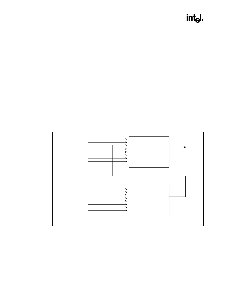
Intel
Æ
82443MX100 PCIset
108
Datasheet
controllers together. IRQ0 is used as a system-timer interrupt and is tied to Interval Timer 1,
Counter 0. IRQ13 is connected internally to FERR#. The remaining 13 interrupt lines (IRQ1,
IRQ3-IRQ12, IRQ14, and IRQ15) are available for external system interrupts. Edge or level-sense
selection is programmable on an individual channel-by-channel basis.
The Interrupt unit also supports interrupt steering. The 440MX can be programmed to allow the
four PCI active low interrupts (PIRQA#-PIRQD#) to be internally routed to one of 11 interrupts:
3-7, 9-12, 14, or 15.
The Interrupt Controller consists of two separate 82C59 cores. Interrupt Controller 1 (CNTRL-1)
and Interrupt Controller 2 (CNTRL-2) are initialized separately and can be programmed to operate
in different modes. The default settings are: 80x86 Mode, Edge Sensitive (IRQ0-15) Detection,
Normal EOI, Non-Buffered Mode, Special Fully Nested Mode disabled, and Cascade Mode.
CNTRL-1 is connected as the Master Interrupt Controller and CNTRL-2 is connected as the Slave
Interrupt Controller.
Note that IRQ13 is generated internally (as part of the coprocessor error support). IRQ12/M is
generated internally (as part of the mouse support) when bit 4 in the XBCS is set to 1. When set to
0, the standard IRQ12 function is provided and IRQ12 appears externally.
Figure 16. Interrupt Controller Block Diagram
INT
(TO CPU)
8 2 C5 9
CORE
CONTROLLER 2
(SLAVE)
0 #
1
2
3
4
5
6
7
8 2 C5 9
CORE
CONTROLLER 1
(MASTER)
0
1
2
3
4
5
6
7
(INTR)
Timer 1 Counter 0
IRQ1
IRQ3
IRQ4
IRQ5
I RQ6
I RQ7
(INTR)
IRQ8#
I RQ9
IRQ10
IRQ11
IRQ12/ M
FERR#
IRQ14
IRQ15
I NTCNTL.drw
Table 69 lists the I/O port address map for the Interrupt Registers.

Intel
Æ
82443MX100 PCIset
Datasheet
109
Table 69. Interrupt Controller Register I/O Port Address Map
Interrupts
I/O Address
Bits (#)
Register
IRQ[7:0]
0020h
8
CNTRL-1 Control Register
IRQ[7:0]
0021h
8
CNTRL-1 Mask Register
IRQ[15:8]
00A0h
8
CNTRL-2 Control Register
IRQ[15:8]
00A1h
8
CNTRL-2 Mask Register
IRQ0, IRQ2, and IRQ13 are connected to the interrupt controllers internally and do not appear
externally. Table 70 lists the typical IRQ functions.
Table 70. Typical Interrupt Functions
Priority
Label
Controller
Typical Interrupt Source
1
IRQ0
1
Interval timer 1, counter 0 OUT
2
IRQ1
1
Keyboard
3-10
IRQ2
1
Interrupt from controller 2
3
IRQ8#
2
Real Time Clock
4
IRQ9
2
Expansion Bus pin B04
5
IRQ10
2
Expansion Bus pin D03
6
IRQ11
2
Expansion Bus pin D04
7
IRQ12/M
2
Mouse interrupt
8
IRQ13
2
Coprocessor Error- FERR#
9
IRQ14
2
Fixed Disk Drive Controller Expansion Bus pin
D07
10
IRQ15
2
Expansion Bus pin D06
11
IRQ3
1
Serial Port 2, Expansion Bus B25
12
IRQ4
1
Serial Port 1, Expansion Bus B24
13
IRQ5
1
Parallel port 2, Expansion Bus B23
14
IRQ6
1
Diskette controller, Expansion Bus B22
15
IRQ7
1
Parallel port 1, Expansion Bus B21
6.10.1.1
Interrupt Sequence
The powerful features of the Interrupt Controller in a microcomputer system are programmability
and interrupt routine addressing capability. The latter allows direct or indirect jumping to the
specific interrupt routine requested without any polling of the interrupting devices. The following
list shows the interrupt sequence for the Intel Architecture (the 8080 mode of the interrupt
controller must never be selected when programming the 440MX).
Note:
Externally, the interrupt acknowledge cycle sequence appears to be different than in a traditional
discrete 82C59 implementation. However, the traditional interrupt acknowledge sequence is
generated within the 440MX and is an ISA-compatible implementation.
1.
One or more of the Interrupt Request lines (IRQx) are raised high, setting the corresponding
IRR bit(s).

Intel
Æ
82443MX100 PCIset
110
Datasheet
2.
The Interrupt Controller evaluates these requests and sends an INTR to the CPU, if
appropriate.
3.
The CPU acknowledges the INTR and responds with two interrupt acknowledge cycles. The
second cycle is translated into a PCI interrupt acknowledge cycle by the Host Bridge. This
command is broadcast over the PCI as a single cycle as opposed to the two-cycle method
typically used.
4.
Upon receiving an interrupt acknowledge cycle from PCI, the 440MX South Bridge/Cluster
converts the single cycle into the two cycles that the internal 8259 pair can respond to with the
expected interrupt vector. The cycle conversion is performed by a functional block in the
440MX Interrupt Controller Unit. The internally generated interrupt acknowledge cycle is
completed as soon as possible, as the Host Bus is held in wait states until the interrupt vector
data is returned. Each cycle appears as an interrupt acknowledge pulse on the INTA# pin of
the cascaded interrupt controllers. These two pulses are not observable at the 440MX
periphery.
5.
Upon receiving the first internally generated interrupt acknowledge pulse, the highest priority
ISR bit is set and the corresponding IRR bit is reset. The Interrupt Controller does not drive
the data bus during this cycle. On the trailing edge of the first cycle pulse, a slave
identification code is broadcast by the master to the slave on a private, internal three-bit wide
bus. The slave controller uses these bits to determine if it must respond with an interrupt
vector during the second INTA# cycle.
6.
Upon receiving the second internally-generated interrupt acknowledge, the Interrupt
Controller releases an 8-bit pointer (the interrupt vector) that the 440MX uses to complete the
PCI cycle in progress. The second CPU interrupt acknowledge cycle can now complete on
the host bus.
7.
This completes the interrupt cycle. In the AEOI mode the ISR bit is reset at the end of the
second interrupt acknowledge cycle pulse. Otherwise, the ISR bit remains set until an
appropriate EOI command is issued at the end of the interrupt subroutine.
If an interrupt request is not present at step four of the sequence (for example, the request was too
short in duration), the Interrupt Controller issues an interrupt level 7.
6.10.1.2
Interrupt Acknowledge Cycle
The CPU generates an interrupt acknowledge cycle that is translated by the Host Bridge into a
single PCI Interrupt Acknowledge. The interrupt controller translates this command into the two
INTA# pulses expected by the interrupt controller subsystem. The Interrupt Controller uses the
first interrupt acknowledge cycle to internally freeze the state of the interrupts for priority
resolution. On the second interrupt acknowledge cycle, the master (CNTRL-1) or slave (CNTRL-
2) sends a byte of data to the processor with the acknowledged interrupt code composed as shown
in Table 71. The byte of data released by the interrupt controller onto the data bus is referred to as
the "interrupt vector."

Intel
Æ
82443MX100 PCIset
Datasheet
111
Table 71. Content of Interrupt Vector Byte for 80x86 System Mode
Interrupt Vector
D7
D6
D5
D4
D3
D2
D1
D0
IRQ7,15
T7
T6
T5
T4
T3
1
1
1
IRQ6,14
T7
T6
T5
T4
T3
1
1
0
IRQ5,13
T7
T6
T5
T4
T3
1
0
1
IRQ4,12
T7
T6
T5
T4
T3
1
0
0
IRQ3,11
T7
T6
T5
T4
T3
0
1
1
IRQ2,10
T7
T6
T5
T4
T3
0
1
0
IRQ1,9
T7
T6
T5
T4
T3
0
0
1
IRQ0,8
T7
T6
T5
T4
T3
0
0
0
NOTE:
T7 - T3 represent the interrupt vector address (refer to the ICW2 Register description).
6.10.1.3
Programming the Interrupt Controller
The Interrupt Controller accepts the following two types of command words generated by the
CPU or bus master:
∑
Initialization Command Words (ICWs)
∑
Operation Command Words (OCWs)
6.10.1.3.1
Initialization Command Words (ICWs)
Before normal operation can begin, each Interrupt Controller in the system must be initialized. In
the 82C59, this is a 2-byte to 4-byte sequence. However, for the 440MX, each controller must be
initialized with a 4-byte sequence. This 4-byte sequence is required to configure the interrupt
controller correctly for 440MX implementation. This implementation is ISA-compatible.
The four initialization command words are referred to by their acronyms: ICW1, ICW2, ICW3,
and ICW4.
The base address for each interrupt controller is a fixed location in the I/O memory space, at
0020h for CNTRL-1 and at 00A0h for CNTRL-2.
An I/O write to the CNTRL-1 or CNTRL-2 base address with data bit 4 equal to 1 is interpreted as
ICW1. For the 440MX-based X-bus systems, three I/O writes to "base address + 1" (021h for
CNTRL-1 and 0A0h for CNTRL-2) must follow the ICW1. The first write to "base address + 1"
(021h/0A0h) performs ICW2, the second write performs ICW3, and the third write performs
ICW4.
∑
ICW1 starts the initialization sequence during which the following events automatically
occur:
1.
Following initialization, an interrupt request (IRQ) input must make a low-to-high
transition to generate an interrupt.
2.
The Interrupt Mask Register is cleared.
3.
IRQ7 input is assigned priority 7.
4.
The slave mode address is set to 7.
5.
Special Mask Mode is cleared and Status Read is set to IRR.

Intel
Æ
82443MX100 PCIset
112
Datasheet
∑
ICW2 is programmed to provide bits [7:3] of the interrupt vector that is released onto the data
bus by the interrupt controller during an interrupt acknowledge. A different base [7:3] is
selected for each interrupt controller. Suggested default values for a typical ISA system are
listed in Table 72.
∑
ICW3 is programmed differently for CNTRL-1 and CNTRL-2 and has a different meaning for
each controller.
For CNTRL-1, the master controller, ICW3 is used to indicate which IRQx input line is used to
cascade CNTRL-2, the slave controller. Within the 440MX interrupt unit, IRQ2 on CNTRL-1 is
used to cascade the INTR output of CNTRL-2. Consequently, bit-2 of ICW3 on CNTRL-1 is set
to a 1 and the other bits are set to 0's.
For CNTRL-2, ICW3 is the slave identification code used during an interrupt acknowledge cycle.
CNTRL-1 broadcasts a code to CNTRL-2 over three internal cascade lines if an IRQ[x] line from
CNTRL-2 won the priority arbitration on the master controller and was granted an interrupt
acknowledge by the CPU. CNTRL-2 compares this identification code to the value stored in
ICW3, and if the code is equal to bits [2:0] of ICW3, CNTRL-2 assumes responsibility for
broadcasting the interrupt vector during the second interrupt acknowledge cycle pulse.
∑
ICW4 must be programmed on both controllers. At the very least, bit 0 must be set to 1 to
indicate that the controllers are operating in an Intel Architecture-based system.
Table 72 lists the typical values programmed by the BIOS at power-up for the 440MX interrupt
controller. Table 72 illustrates the sequence the software must follow to load the ICWs. The
sequence must be executed for CNTRL-1 and CNTRL-2. ICW1, ICW2, ICW3, and ICW4 must
be written in order. Any divergence from this sequence, such as an attempt to program an OCW,
will result in improper initialization of the interrupt controller and unexpected, erratic system
behavior. It is suggested that CNTRL-2 be initialized first, followed by CNTRL-1.
In the 440MX, it is required that all four ICWs be initialized.
Table 72. Suggested Default Values for ICW Registers
Port
Value
Contents
020h
11h
CNTLR-1, ICW1
021h
08h
CNTLR-1, ICW2 Vector Address for 000020h
021h
04h
CNTLR-1, ICW3 Indicates Slave Connection
021h
01h
CNTLR-1, ICW4 8086 Mode
021h
B8h
CNTLR-1, Interrupt Mask (may vary)
0A0h
11h
CNTLR-2, ICW1
0A1h
70h
CNTLR-2, ICW2 Vector Address for 0001C0h
0A1h
02h
CNTLR-2, ICW3 Indicates Slave ID
0A1h
01h
CNTLR-2, ICW4 8086 Mode
0A1h
BDh
CNTLR-2, Interrupt Mask (may vary)

Intel
Æ
82443MX100 PCIset
Datasheet
113
Figure 17. Initialization Sequence for the 440MX ICW Modes of Operation
ICW3
IS ICW4
NEEDED?
ICW4
READY TO ACCEPT
INTERRUPT REQUESTS
YES (IC4=1)
YES (SNGL=0)
ICW2
IN CASCADE
MODE?
SIO-04.drw
ICW1
CNTRL-1
CNTRL-2
I/O Address
Special Conditions
020h
0A0h
D4 = 1
021h
0A1h
Must immediately follow
ICW2 Access
021h
0A1h
Must immediately follow
ICW1 Access
021h
0A1h
Must immediately follow
ICW3 Access
6.10.1.3.2
Operation Command Words (OCWs)
OCWs are command words that dynamically reprogram the Interrupt Controller to operate in
various interrupt modes. OCWs can be written to the Interrupt Controller any time after
initialization. The three Operation Command Words are referred to by their acronyms: OCW1,
OCW2, and OCW3.
∑
Any interrupt lines can be masked by writing an OCW1. A 1 written to any bit of this
command word masks the incoming interrupt requests on the corresponding IRQx line.
∑
OCW2 is used to control the rotation of interrupt priorities when operating in the rotating
priority mode and to control the End of Interrupt (EOI) function of the controller.
∑
OCW3 is used to set up reads of the ISR and IRR, to enable or disable the Special Mask
Mode (SMM), and to set up the interrupt controller in polled interrupt mode.
As shown in Figure 17 all ICWs must be programmed prior to programming the OCWs.

Intel
Æ
82443MX100 PCIset
114
Datasheet
6.10.1.4
End-of-Interrupt Operation
6.10.1.4.1
End of Interrupt (EOI)
The In Service (IS) bit can be set to 0 automatically following the trailing edge of the second
INTA# pulse (when AEOI bit in ICW1 is set to 1) or by a command word that must be issued to
the Interrupt Controller before returning from a service routine (EOI command). An EOI
command must be issued twice with this cascaded interrupt controller configuration, once for the
master and once for the slave.
There are two forms of EOI commands: Specific and Non-Specific. When the Interrupt Controller
is operated in modes that preserve the fully nested structure, it can determine which IS bit to set to
0 on EOI. When a Non-Specific EOI command is issued, the Interrupt Controller automatically
sets to 0 the highest IS bit of those that are set to 1, since in the fully nested mode the highest IS
level was necessarily the last level acknowledged and serviced. A non-specific EOI can be issued
with OCW2 (EOI=1, SL=0, R=0).
When a mode is used that may disturb the fully nested structure, the Interrupt Controller may no
longer be able to determine the last level acknowledged. In this case, a Specific EOI must be
issued which includes as part of the command the IS level to be reset. A specific EOI can be
issued with OCW2 (EOI=1, SL=1, R=0, and LO-L2 is the binary level of the IS bit to be set to 0).
It should be noted that an IS bit that is masked by an IMR bit will not be cleared by a non-specific
EOI if the Interrupt Controller is in the Special Mask Mode.
6.10.1.4.2
Automatic End of Interrupt (AEOI) Mode
If AEOI=1 in ICW4, then the Interrupt Controller operates in AEOI mode continuously until
reprogrammed by ICW4. Note that reprogramming ICW4 implies that ICW1, ICW2, and ICW3
must be reprogrammed first, in sequence. In AEOI mode, the Interrupt Controller automatically
performs a non-specific EOI operation at the trailing edge of the last interrupt acknowledge pulse.
Note that from a system standpoint, this mode should be used only when a nested multi-level
interrupt structure is not required within a single Interrupt Controller. The AEOI mode can only be
used in a master Interrupt Controller and not a slave (on CNTRL-1, but not CNTRL-2).
6.10.1.4.3
Fully Nested Mode
The Fully Nested mode is entered after initialization unless another mode is programmed. The
interrupt requests are ordered in priority from 0 through 7 (0 being the highest). When an interrupt
is acknowledged, the highest priority request is determined and its vector placed on the bus.
Additionally, a bit in the Interrupt Service Register (IS[0:7]) is set. This IS bit remains set until the
microprocessor issues an End of Interrupt (EOI) command immediately before returning from the
service routine. Or, if the AEOI (Automatic End of Interrupt) bit is set, this IS bit remains set until
the trailing edge of the second INTA#. While the IS bit is set, all further interrupts of the same or
lower priority are inhibited, while higher levels generate an interrupt (which is acknowledged only
if the microprocessor internal interrupt enable flip-flop has been re-enabled through software).
After the initialization sequence, IRQ0 has the highest priority and IRQ7 the lowest. Priorities can
be changed in the rotating priority mode, as explained later in this section.

Intel
Æ
82443MX100 PCIset
Datasheet
115
6.10.1.4.4
The Special Fully Nested Mode
This mode is used in the case of a system where cascading is used, and the priority has to be
conserved within each slave. In this case, the special fully nested mode is programmed to the
master (using ICW4). This mode is similar to the normal nested mode with the following
exceptions:
∑
When an interrupt request from a certain slave is in service, this slave is not locked out from
the master's priority logic and further interrupt requests from higher priority IRQs within the
slave are recognized by the master and initiate interrupts to the processor. (In the normal
nested mode, a slave is masked out when its request is in service and no higher requests from
the same slave can be serviced.)
∑
When exiting the Interrupt Service routine, the software must check whether the interrupt
serviced was the only one from that slave. This is done by sending a non-specific End of
Interrupt (EOI) command to the slave and then reading its In-Service Register and checking
for zero. If it is empty, a non-specific EOI can also be sent to the master. If not, no EOI
should be sent.
6.10.1.4.5
Automatic Rotation (Equal Priority Devices)
In some applications, a number of interrupting devices have equal priority. Automatic rotation
mode provides for a sequential 8-way rotation. In this mode, a device receives the lowest priority
after being serviced. In the worst case, a device requesting an interrupt must wait until each of
seven other devices are serviced at most once. Figure 18 illustrates an example of automatic
rotation.
Figure 18. Automatic Rotation Mode Example
If the priority and "in
service" status is:
After Rotate
(IRQ4 was serviced, all other priorities rotated correspondingly)
2
1
0
7
6
5
4
3
Priority
Status
Highest Priority
IS7 IS6
IS5 IS4 IS3 IS2 IS1
IS0
0
1
0
0
0
0
0
0
"IS" Status
Lowest Priority
SIO-05.drw
7
6
5
4
3
2
1
0
Priority
Status
Lowest
Priority
Highest
Priority
Before Rotate
(IRQ4 the highest priority requiring service)
IS7 IS6
IS5 IS4 IS3 IS2 IS1
IS0
0
1
0
1
0
0
0
0
"IS" Status
There are two ways to accomplish automatic rotation using OCW2; the Rotation on Non-Specific
EOI Command (R=1, SL=0, EOI=1) and the Rotate in Automatic EOI Mode which is set by (R=1,
SL=0, EOI=0) and cleared by (R=0, SL=0, EOI=0).

Intel
Æ
82443MX100 PCIset
116
Datasheet
6.10.1.4.6
Specific Rotation (Specific Priority)
The programmer can change priorities by programming the bottom priority and thus fixing all
other priorities. For example, if IRQ5 is programmed as the bottom priority device, then IRQ6 is
the highest priority device.
The Set Priority Command is issued in OCW2 where: R=1, SL=1; LO-L2 is the binary priority
level code of the bottom priority device. See the register description for bit definitions.
Note that, in this mode, internal status is updated by software control during OCW2. However, it
is independent of the End of Interrupt (EOI) command (also executed by OCW2). Priority changes
can be executed during an EOI command by using the Rotate on Specific EOI Command in
OCW2 (R=1, SL=1, EOI=1, and LO-L2=IRQ level to receive bottom priority).
6.10.1.4.7
Poll Command
The Polled Mode can be used to conserve space in the interrupt vector table. Multiple interrupts
that can be serviced by one interrupt service routine do not need separate vectors if the service
routine uses the poll command.
The Polled Mode can also be used to expand the number of interrupts. The polling interrupt
service routine can call the appropriate service routine, instead of providing the interrupt vectors in
the vector table.
In this mode, the INTR output is not used and the microprocessor internal Interrupt Enable flip-
flop is reset, disabling its interrupt input. Service to devices is achieved by the software using a
Poll command.
The Poll command is issued by setting P=1 in OCW3. The Interrupt Controller treats the next I/O
read pulse to the Interrupt Controller as an interrupt acknowledge, sets the appropriate IS bit if
there is a request, and reads the priority level. Interrupts are frozen from the I/O write to the I/O
read.
Figure 19 shows the words enabled onto the data bus during an I/O read. The polled mode is
useful if there is a routine command common to several levels so that the INTA# sequence is not
needed (saves ROM space).
Figure 19. Polled Mode
1
--
--
--
--
W2
W1
W0
D7
D6
D5
D4
D3
D2
D1
D0
SIO-06.DRW
NOTES:
W0-W2: Binary code of the highest priority level requesting service.
Bit D7 -- I:Equal to 1 if there is an interrupt.

Intel
Æ
82443MX100 PCIset
Datasheet
117
6.10.1.4.8
Cascade Mode
The Interrupt Controllers in the 440MX are interconnected in a cascade configuration with one
master and one slave. This configuration can handle up to 15 separate priority levels.
The master controls the slaves through a three-line internal cascade bus. When the master drives
010b on the cascade bus, this bus acts like a chip select to the slave controller.
In a cascade configuration, the slave interrupt outputs are connected to the master interrupt request
inputs. When a slave request line is activated and afterwards acknowledged, the master enables the
corresponding slave to release the interrupt vector address during the second INTA# cycle of the
interrupt acknowledge sequence.
Each Interrupt Controller in the cascaded system must follow a separate initialization sequence
and can be programmed to work in a different mode. An EOI Command must be issued twice:
once for the master and once for the slave.
6.10.1.4.9
Edge and Level Triggered Mode
In X-bus systems this mode is programmed using bit 3 in ICW1. With the 440MX this bit is
disabled and a new register for Edge and Level Triggered mode selection, per interrupt input, is
included. These are the Edge/Level control Registers ELCR1 and ELCR2. The default
programming is equivalent to programming the LTIM bit (ICW1 bit 3) to a 0 (all interrupts
selected for Edge Triggered mode). Note that IRQ0, 1, 2, 8#, and 13 cannot be programmed for
Level Sensitive mode and cannot be modified by software.
If an ELCR bit = "0," an interrupt request is recognized by a low-to-high transition on the
corresponding IRQx input. The IRQ input can remain high without generating another interrupt.
If an ELCR bit = "1," an interrupt request is recognized by a low level on the corresponding IRQ
input and there is no need for an edge detection. The interrupt request must be removed before the
EOI command is issued to prevent a second interrupt from occurring.
In both the Edge and Level Triggered modes, the IRQ inputs must remain active until after the
falling edge of the first INTA#. If the IRQ input goes inactive before this time, a default IRQ7
occurs when the CPU acknowledges the interrupt. This can be a useful safeguard for detecting
interrupts caused by spurious noise glitches on the IRQ inputs. To implement this feature, the
IRQ7 routine is used for "clean up" by simply executing a return instruction, and thus ignoring the
interrupt. If IRQ7 is needed for other purposes, a default IRQ7 can still be detected by reading the
ISR. A normal IRQ7 interrupt sets the corresponding ISR bit; a default IRQ7 does not set this bit.
If a default IRQ7 routine occurs during a normal IRQ7 routine, however, the ISR remains set. In
this case, it is necessary to keep track of whether or not the IRQ7 routine was previously entered.
If another IRQ7 occurs, it is a default.
6.10.1.5
Register Functionality
For a detailed description of the Interrupt Controller Register set, refer to the Interrupt Controller
Register description in the Register Description section.
6.10.1.6
Interrupt Masks

Intel
Æ
82443MX100 PCIset
118
Datasheet
6.10.1.6.1
Masking on an Individual Interrupt Request Basis
Each interrupt request input can be masked individually by the Interrupt Mask Register (IMR).
This register is programmed through OCW1. Each bit in the IMR masks one interrupt channel, if
it is set to a 1. Bit 0 masks IRQ0, Bit 1 masks IRQ1, and so forth. Masking an IRQ channel does
not affect the other channel's operation, with one exception: Masking IRQ2 on CNTRL-1 masks
off all requests for service from CNTRL-2. The CNTRL-2 INTR output is physically connected to
the CNTRL-1 IRQ2 input.
6.10.1.6.2
Special Mask Mode
Some applications may require an interrupt service routine to dynamically alter the system priority
structure during its execution under software control. For example, the routine may wish to inhibit
lower priority requests for a portion of its execution but enable some of them for another portion.
The difficulty is that if an Interrupt Request is acknowledged and an End of Interrupt command
did not reset its IS bit (for example, while executing a service routine), the Interrupt Controller
would have inhibited all lower priority requests with no easy way for the routine to enable them.
The Special Mask mode enables all interrupts not masked by a bit set in the Mask Register.
Interrupt service routines that require dynamic alteration of interrupt priorities can take advantage
of the Special Mask mode. For example, a service routine can inhibit lower priority requests
during a part of the interrupt service, then enable some of them during another part.
In the Special Mask mode, when a mask bit is set to 1 in OCW1, it inhibits further interrupts at
that level and enables interrupts from all other levels (lower as well as higher) that are not masked.
Thus, any interrupts may be selectively enabled by loading the Mask Register with the appropriate
pattern.
Without Special Mask mode, if an interrupt service routine acknowledges an interrupt without
issuing an EOI to clear the IS bit, the interrupt controller inhibits all lower priority requests. The
Special Mask mode provides an easy way for the interrupt service routine to selectively enable
only the interrupts needed by loading the Mask Register.
Special Mask mode is set by OCW3 where: SSMM=1, SMM=1, and cleared where SSMM=1,
SMM=0.
6.10.1.7
Reading the Interrupt Controller Status
The input status of several internal registers can be read to update the user information on the
system. The Interrupt Request Register (IRR) and In-Service Register (ISR) can be read via
OCW3. The Interrupt Mask Register (IMR) is read via a read of OCW1. This section briefly
describes IRR, ISR, and IMR.
∑
Interrupt Request Register (IRR): This 8-bit register that contains the status of each interrupt
request line. Bits that are clear indicate interrupts that have not requested service. The
Interrupt Controller clears the IRR's highest priority bit during an interrupt acknowledge
cycle. (Not affected by IMR.)
∑
In-Service Register (ISR): This 8-bit register indicates the priority levels currently receiving
service. Bits that are set indicate interrupts that have been acknowledged and their interrupt
service routine started. Bits that are cleared indicate interrupt requests that have not been
acknowledged, or interrupt request lines that have not been asserted. Only the highest priority

Intel
Æ
82443MX100 PCIset
Datasheet
119
interrupt service routine executes at any time. The lower priority interrupt services are
suspended while higher priority interrupts are serviced. The ISR is updated when an End of
Interrupt Command is issued.
∑
Interrupt Mask Register (IMR): This 8-bit register indicates which interrupt request lines are
masked.
The IRR can be read when, prior to the I/O read cycle, a Read Register Command is issued with
OCW3 (RR=1, RIS=0).
The ISR can be read when, prior to the I/O read cycle, a Read Register Command is issued with
OCW3 (RR=1, RIS=1).
The interrupt controller retains the ISR/IRR status read selection following each write to OCW3.
Therefore, there is no need to write an OCW3 before every status read operation, as long as the
current status read corresponds to the previously selected register. For example, if the ISR is
selected for status read by an OCW3 write, the ISR can be read over and over again without
writing to OCW3 again. However, to read the IRR, OCW3 must be reprogrammed for this status
read prior to the OCW3 read to check the IRR. This is not true when poll mode is used. Polling
Mode overrides status read when P=1, RR=1 in OCW3.
After initialization the Interrupt Controller is set to read the IRR.
As stated, OCW1 is used to read the IMR. The output data bus contains the IMR status whenever
I/O read is active and the address is 021h or 061h (OCW1).
6.10.1.8
Interrupt Steering
The 440MX can be programmed to allow four PCI programmable interrupts (PIRQA#-PIRQD#)
to be internally routed to one of 11 interrupts: 3-7, 9-12, 14, or 15. PCLK is used to synchronize
the PIRQx# inputs. The PIRQx# lines are run through an internal multiplexer that assigns, or
routes, an individual PIRQx# line to any one of 11 IRQ inputs (see Figure 20 for an illustration of
the interrupt steering logic). The assignment is programmable through the PIRQx Route Control
Registers. One or more PIRQx# lines can be routed to the same IRQx input. If interrupt steering is
not required, the Route Registers can be programmed to disable steering.
Bits 0-3 in each PIRQx Route Control Register are used to route the associated PIRQx# line to an
internal IRQ input. Bit 7 in each register is used to disable routing of the associated PIRQx#.
The PIRQx# lines are defined as active low, level sensitive to allow multiple interrupts on a PCI
Board to share a single line across the connector. When a PIRQx# is routed to specified IRQ line,
the software must change the IRQ's corresponding ELCR bit to Level Sensitive mode. This means
that the selected IRQ can no longer be used by an X-bus device, unless that X-bus device can
respond as an active low-level sensitive interrupt.

Intel
Æ
82443MX100 PCIset
120
Datasheet
Figure 20. Section of Interrupt Steering Logic
(Without Serial IRQ)
PIRQ#
I RQ1 5
I RQ1 4
IRQ11
I RQ1 0
PI RQx# Contr ol
Regi s t er s
I RQ1 3
IRQ7
I RQ6
IRQ5
IRQ4
IRQ3
IRQ1
Timer/Count er
82C59
82C59
8
9
1 0
1 1
1 2
1 3
14
15
0
1
2
3
4
5
6
7
MBIRQ control
Regi sters
I R Q0
inv
IRQ12/M
IRQ9
IRQ8#
sync
Decoder
(ABCD)
4
6.10.2
Serial IRQ Scheme
For more information about the serial IRQ scheme, see the Serialized IRQ Support for PCI
Systems Rev 6.0.

Intel
Æ
82443MX100 PCIset
Datasheet
121
6.10.2.1
Overview
The 440MX supports a serial IRQ scheme that allows a single signal to be used to report ISA-style
interrupt requests. This scheme is typically used in a mobile environment by docking bridges or
CardBus controllers.
Because more than one device may need to share the single serial IRQ signal, an Open-collector
signaling scheme is used. Timing is based on the PCI clock. If the PCI clock is shut when a
device needs to signal an interrupt, the CLKRUN# signal must first be activated to restart the PCI
clock.
The serial IRQ configuration is handled via the PCI configuration space. No other registers are
associated with the scheme.
6.10.2.2
Protocol
Serial interrupt information is transferred using three frame types: a Start Frame, one or more IRQ
Data frames, and one Stop frame. There are also two modes of operation: Quiet Mode and
Continuous Mode.
6.10.2.2.1
Quiet (Active) Mode
To indicate an interrupt, the peripheral drives the SERIRQ signal active for one clock and then
three-states it, which transitions all state machines from the IDLE to ACTIVE states.
The 440MX then takes control of the SERIRQ signal by driving it low on the next clock, and
continues driving it low for 3-7 more clocks (programmable). Thus, the total number of clocks
SERIRQ is low is 4-8. After those clocks, the 440MX drives SERIRQ high for one clock and then
three-states the signal.
6.10.2.2.2
Continuous (Idle) Mode
In this mode, the 440MX initiates the START frame rather than the peripherals. Typically this is
done to update the IRQ status (acknowledges). The 440MX drives SERIRQ low for 4-8 clocks.
This is the default mode after reset, and can be used to enter the Quiet mode.
6.10.2.2.3
Data Frame
After the Start frame is initiated, all SERIRQ peripherals must start counting frames based on the
rising edge of SERIRQ. Each of the IRQ/DATA frames has exactly three phases of 1 clock each:
a Sample phase, a Recovery Phase, and a Turn-around phase.
During the Sample phase, the SERIRQ device drives SERIRQ low if the corresponding interrupt
signal should be active. If the corresponding interrupt is inactive, then the SERIRQ devices
should not drive the SERIRQ signal. It remains high due to pull-up resistors.
Note:
The 440MX ignores the state of the IRQ0 signal. This may preclude using a Timer/Counter chip
outside of the 440MX. However, that configuration is not supported by any previous Intel PCIset.
During the other two phases (Turn-around and Recovery), no device should drive the SERIRQ
signal. The IRQ/DATA frames have a specific order and usage, as shown in Table 73.

Intel
Æ
82443MX100 PCIset
122
Datasheet
Table 73. SIRQ Frames
Data Frame Number
Usage
# Clocks Past Start
Notes
1
IRQ0
2
Not supported by the 440MX.
2
IRQ1
5
3
SMI#
8
Causes EXSMI# to go active
4
IRQ3
11
5
IRQ4
14
6
IRQ5
17
7
IRQ6
20
8
IRQ7
23
9
IRQ8
26
10
IRQ9
29
11
IRQ10
32
12
IRQ11
35
13
IRQ12
38
14
IRQ13
41
15
IRQ14
44
16
IRQ15
47
17
IOCHCK#
50
Not Supported
18
PCI INTA#
53
Supported
19
PCI INTB#
56
Supported
20
PCI INTC#
59
Supported
21
PCI INTD#
62
Supported
22-32
Unassigned
96
Not Supported
The 440MX is not required to broadcast internal interrupt states. This greatly reduces the amount
of transitions on the SERIRQ signal and simplifies the state machine.
6.10.2.2.4
Stop Frame
After all of the data frames, the 440MX performs a Stop Frame, which is done by making
SERIRQ low for 2-3 clocks. The number of clocks determines the next mode:
∑
If SERIRQ is low for 2 clocks, then the next mode is the Quite mode. Any SERIIRQ device
may initiate a Start Frame in the second clock (or more) after the rising edge of the Stop
Frame.
∑
If SERIRQ is low for 3 clocks, then the next mode is the Continuous mode. Only the 440MX
may initiate a Start Frame in the second clock (or more) after the rising edge of the Stop
Frame.
6.10.2.3
SMI# Via SERIRQ
When an SMI# is indicated via SERIRQ, the 440MX drives its EXSMI# signal active. This in
turn causes SMI# to go active. The BIOS sees EXSMI# go active, with no corresponding status

Intel
Æ
82443MX100 PCIset
Datasheet
123
bit set in the peripheral. The BIOS can then check the devices connected to the SERIRQ signal to
find the cause of the SMI#.
6.10.2.4
SERIRQ ORing with ISA IRQ
The 440MX internally OR's the output of the SERIRQ decoder with the ISA IRQ signals. The
PnP software should ensure that two separate devices are not programmed to use the same ISA
IRQ signals, unless the drivers are set up for interrupt sharing. Otherwise, this could result in
unpredictable operation and is already a system limitation.
6.11
USB Host Controller
The 440MX contains a USB Host Controller (HC), which includes a root hub with two USB ports.
This permits connection of two USB peripheral devices directly to the 440MX without an external
hub. If more devices are required, an external hub can be connected to either of the built-in ports.
The USB's PCI Configuration Registers are located in Function 2, PCI configuration space.
The Host Controller completely supports the standard Universal Host Controller Interface (UHCI)
and thus, takes advantage of the standard software drivers written to be compatible with UHCI.
Figure 21 shows a conceptual view of a USB system. The UHCI consists of two parts-- Host
Controller Driver (HCD) and Host Controller (HC). The Host Controller interfaces to the USB
system software in the host via the HCD. The HCD software manages the Host Controller
operation and is responsible for scheduling the traffic on USB by posting and maintaining
transactions in system memory. HCD is part of the system software and is typically provided by
the operating system vendor. HCD provides the software layer between the Host Controller and
the USBD software layer (also located in the operating system). The UHCI's HCD software
interprets requests from the USBD and builds Frame List, Transfer Descriptor, Queue Head, and
data buffer data structures for the Host Controller. The data structures are built-in system memory
and contain all necessary information to provide end-to-end communication between client
software in the host and devices on the USB.
The Host Controller moves data between system memory and devices on the USB by processing
these data structures and generating the transaction on the USB. The Host Controller executes the
schedule lists generated by the HCD and reports the status of transactions on the USB to the HCD.
Command execution includes generating serial bus token and data packets based on the command
and initiating transmission on USB. For commands that require the Host Controller to receive data
from the USB device, the Host Controller receives the data and then transfers it to the system
memory pointed to by the command. The UHCI's HCD provides sufficient commands and data to
keep ahead of the Host Controller execution and analyzes the results as the commands are
completed.
For additional information on the functionality of the USB Host Controller, refer to the Universal
Host Controller Interface (UHCI) Design Guide, Revision 1.1 (Order number 297650-002). Note
that the UHCI Design Guide refers to USB ports 1 and 2. The 440MX USB ports are ports 0 and
1, respectively.
Additions to the 440MX USB interface beyond UHCI Revision 1.1 include support for over-
current detection on USB ports 0 and 1. If an over-current condition is detected on a USB port,
that port will be disabled. Bits 10:11 in each Port Status and Control Register are used to report
over-current conditions.

Intel
Æ
82443MX100 PCIset
124
Datasheet
Figure 21. USB System Conceptual View
Client Software
Universal Serial Bus Driver
(USBD)
Universal Host Controller
Driver (HCD)
Universal Host Controller (HC)
USB Device
USB Device
USB
USB
Universal Host
Controller Interface
(UHCI)
Hardware
Software
usb_blk
6.12
IDE Interface
The 440MX integrates a high performance PCI-to-IDE interface, which has one physical channel
adapter and supports two drives (drive 0 and drive 1). This interface is capable of accelerated PIO
data transfers as well as acting as a PCI bus master on behalf of an IDE DMA slave device. The
440MX provides an interface for a single IDE connector.
All IDE data transfer command strobes, DMA request and grant signals, address and data lines,
and the PIORDY signal interface directly to the 440MX. These lines correspond to the Primary
IDE channel.
Only PCI masters have access to the IDE port. Memory targeted by the IDE interface acting as a
PCI bus master on behalf of IDE DMA slaves must reside on the PCI or in the main memory
implemented by the 440MX.
Although a physical Secondary IDE channel interface does not exist on the 440MX, all of the
configuration I/O ports still exist and are claimed, if enabled, by the 440MX. The BIOS is
expected to disable this channel. The 440MX does not support swap bay.
6.12.1
ATA Register Block Decode
The IDE ATA I/O ports are decoded by the 440MX when the COM[IOSE] bit is set to one, as
well as IDETIMP[IDE] and IDETIMS[IDE]. (ATA stands for "AT Attachment," the specification
for AT-compatible drive interfaces). The actual ATA registers are implemented in the drive itself.
An access to an IDE register results in the assertion of the appropriate chip select for that register.

Intel
Æ
82443MX100 PCIset
Datasheet
125
The transaction is then run using compatible timing and using the IDE command strobes
(PDIOR#, PDIOW#).
There are two I/O ranges: the Command block, which corresponds to the CS1# chip select, and the
Control Block, which corresponds to the CS3# chip select. The Command block is an 8-byte
range, while the Control Block is a 4-byte range. The upper 16 bits of the I/O address are decoded
as all zeros.
Command Block Offset: 01F0h for Primary, 0170h for Secondary
Control Block Offset:
03F4h for Primary, 0374h for Secondary
Table 74 and Table 75 specify the Command Block and Control Block Registers respectively, as
they affect the 440MX hardware definition. See the AT Attachment Specification for more details.
Table 74. IDE Legacy I/O Ports: Command Block Registers (CS1x# Chip Select)
I/O Offset
Register Function (Read / Write)
Register Access
00h
Data
R/W
01h
Error / Features
R/W
02h
Sector Count
R/W
03h
Sector Number
R/W
04h
Cylinder Low
R/W
05h
Cylinder High
R/W
06h
Drive / Head
R/W
07h
Status / Command
R/W
The Data Register is accessed as a 16-bit register for PIO transfers (except for ECC bytes). All
other registers should always be accessed as 8-bit quantities by software.
Table 75. IDE Legacy I/O Port Definition: Control Block Registers (CS3x# Chip Select)
I/O Offset
Register Function (Read / Write)
Register Access
00h
Reserved
Reserved
01h
Reserved
Reserved
02h
Alt Status / Device control
R/W
03h
Forward to X-bus (Floppy)
R/W
The 440MX claims all accesses to these ranges, if enabled. The byte enables do not have to be
externally decoded to assert DEVSEL#. Accesses to byte 3 of the Control Block are forwarded to
the X-bus, where the Floppy controller responds. A 16-bit access to offset 02h of the Control
Block (byte enables 2 and 3 asserted) results in a Target Abort.
Each of the two drives (drive 0 or 1) on a cable implements separate ATA register files. To
determine the targeted drive, the 440MX shadows the value of bit 4 (drive bit) of byte 6
(Drive/Head Register) of the ATA Command Block (CS1x#) for the IDE connector.
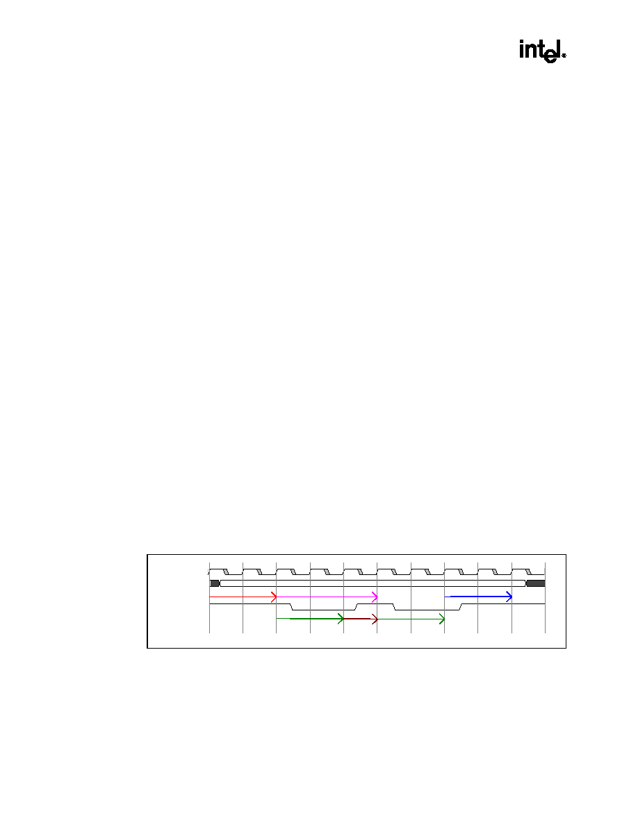
Intel
Æ
82443MX100 PCIset
126
Datasheet
6.12.2
PIO IDE Transactions
The 440MX IDE controller includes both compatible and fast timing modes. The fast timing
modes can be enabled only for the IDE data ports. All other transactions to the IDE registers are
run in single transaction mode with compatible timings. The 440MX IDE signals are controlled
with the granularity of the PCI clock.
Up to two IDE devices may be attached to the IDE connector (drive 0 and drive 1). The IDETIM
and SIDETIM Registers permit different timing modes to be programmed for drive 0 and drive 1
of the connector.
The Ultra DMA/33 synchronous DMA timing modes can also be applied to each drive by
programming the SDMACTL and SDMATIM Registers. When a drive is enabled for
synchronous DMA mode operation, the DMA transfers are executed with the synchronous DMA
timings. The PIO transfers are executed using compatible timings or fast timings if also enabled.
6.12.3
PIO IDE Timing Modes
IDE data port transaction latency consists of startup latency, cycle latency, and shutdown latency.
Startup latency is incurred when a PCI master cycle targeting the IDE data port is decoded and the
PDA[2:0] and CSxx# lines are not set up. Startup latency provides the setup time for the
PDA[2:0] and CSxx# lines prior to assertion of the read and write strobes (PDIOR# and
PDIOW#).
Cycle latency consists of the I/O command strobe assertion length and recovery time. Recovery
time is provided so that transactions may occur back-to-back on the IDE interface (without
incurring startup and shutdown latency) without violating the minimum cycle periods for the IDE
interface. The command strobe assertion width for the enhanced timing mode is selected by the
IDETIM Register and may be set to 2, 3, 4, or 5 PCI clocks. The recovery time is selected by the
IDETIM Register and may be set to 1, 2, 3, or 4 PCI clocks. Figure 22 shows how these latencies
are related and how they are summed to produce the overall transaction latency.
Figure 23 the case where the PIORDY Sample Point (ISP) is set to two clocks (minimum) and the
Recovery Time (RCT) is set to one clock (minimum).
Figure 22. Enhanced IDE Timing Mode Components
valid and stable
PCLK
PDA[2:0], CSxx#
PDIOx#
startup latency
cycle period
shutdown latency
PIORDY sample point
recovery time
PIORDY sample point
[ISP]
[RCT]
[ISP]

Intel
Æ
82443MX100 PCIset
Datasheet
127
Figure 23. Inserting Wait States by Deasserting PIORDY
PCLK
PIORDY
PDIOx#
a
b
a
b
b
PIORDY Sample Point (ISP)
Recovery Time (RCT)
wait states
If PIORDY is asserted when the initial sample point is reached, no wait states are added to the
command strobe assertion length. If PIORDY is negated when the initial sample point is reached,
additional wait states are added. Since the rising edge of PIORDY must be synchronized, at least
two additional PCI clocks are added.
Shutdown latency is incurred after outstanding scheduled IDE data port transactions (either a non-
empty write post buffer or an outstanding read prefetch cycle) have completed and before other
transactions can proceed. It provides hold time on the PDA[2:0] and CXxx# lines with respect to
the read and write strobes (PDIOR# and PDIOW#). Shutdown latency is 2 PCI clocks in duration.
Table 76 shows the timings for various IDE transactions. It is important to note that the ICRT
(ISA Controller Recovery Timer) Register (Config Register 4Ch) does not affect the IDE data
ports when fast timing modes are enabled. Specifically, setting bit 2 (16-bit I/O recovery enable)
should not add wait states to IDE data port read accesses when any of the fast timing modes are
enabled.
Table 76. Command Strobe Width for IDE Transaction Types
IDE Transaction Type
Startup
Latency
ISP
RCT
Shutdown
Latency
30-33 MHz non data port (8-
bit)
4
11
22
2
30-33 MHz data port (16-bit)
3
6
14
2
Enhanced timing data port
2
2-5
1-4
2
NOTE:
Command strobe widths are in PCI clock units.
Note:
Startup and Recovery latencies are incurred for all IDE PIO transactions, EXCEPT enhanced
timing data port transactions. Further, the IDE chip selects are guaranteed to be deasserted for at
least two clocks after the deassertion of the I/O strobe for the last transaction and before the
Startup latency of the next.
6.12.4
Enhanced Timing Modes
The IDE interface implemented by the 440MX includes fast timing modes that target local bus
implementations. These timing modes are faster than those possible with ISA-based
implementations and are controlled with the granularity of the PCI clock.

Intel
Æ
82443MX100 PCIset
128
Datasheet
The fast timing modes may be enabled only for the IDE data ports. All other transactions to the
IDE registers are run in single transaction mode with compatible timings.
Up to two IDE devices may be attached to the IDE connector (drive 0 and drive 1). The timing
mode for the drives is selected via several registers.
When the IDETIMx[SITRE] bit is disabled, one fast timing mode can be applied to one or both
drives by programming the IDETIMx[ISP] and IDETIMx[RCT] fields as shown in Table 77. Fast
Timing mode may be applied to drive 0, drive 1, or both, by setting the IDETIMx[TIME0] and/or
the IDETIMx[TIME1] bits. Transactions targeting the other drive use compatible timing. When
the IDETIMx[SITRE] bit is enabled, a fast timing mode can be selected for each drive by
programming the IDETIMx and SIDETIM Registers. Table 77 identifies how these bits can be
programmed for Drive 0 and Drive 1 timing mode selection.
Table 77. IDETIMx Timing Modes for Drives 0 and 1
IDETIMx
[SITRE]
IDETIMx
[TIME0]
IDETIMx
[TIME1]
Drive 0
Timing
Drive 1
Timing
0
0
0
Compatible
Compatible
0
0
1
Compatible
IDETIMx[ISP/RCT]
0
1
0
IDETIMx[ISP/RCT]
Compatible
0
1
1
IDETIMx[ISP/RCT]
IDETIMx[ISP/RCT]
1
0
0
Compatible
Compatible
1
0
1
Compatible
SIDETIM[ISP/RCT]
1
1
0
IDETIMx[ISP/RCT]
Compatible
1
1
1
IDETIMx[ISP/RCT]
SIDETIM[ISP/RCT]
The synchronous DMA timing mode can also be applied independently to each drive by
programming the SDMAC and SDMATIM Registers. When a particular drive is programmed for
Sync DMA mode (SYNCDMA and SDMATIM Registers) AND a fast timing mode (IDETIMx or
SIDETIM Register), DMA transfers are processed using the Sync DMA timing mode and PIO
transfers are processed using the fast timing mode.
6.12.4.1
PIORDY Masking
When the IDETIMx[IE0] or IDETIMx[IE1] bits are "0" the external PIORDY signal is ignored
and the internal PIORDY signal is assumed asserted at the first ISP sample point.
6.12.4.2
PIO 32-Bit IDE Data Port Accesses
A 32-bit PCI transaction run to the IDE data address results in two back-to-back 16-bit
transactions to the IDE data port. The 32-bit data port feature is enabled for all timings, not just
enhanced timing. For compatible timings, a shutdown and startup latency is incurred between the
two 16-bit halves of the IDE transaction, which guarantees that the chip selects will be negated for
at least two PCI clocks between the two cycles.

Intel
Æ
82443MX100 PCIset
Datasheet
129
6.12.4.3
PIO IDE Data Port Prefetching and Posting
The 440MX can be programmed via the IDETIM Registers to allow data to be posted to and
prefetched from the IDE data ports. Data prefetching is initiated when a data port read occurs.
The read prefetch eliminates latency to the IDE data ports and allows them to perform back-to-
back for the highest possible PIO data transfer rates. The first data port read of a sector is called
the demand read. Subsequent data port reads from the sector are called prefetch reads. The
demand read and all prefetch reads must be of the same size (16 or 32 bits).
Data posting is performed for writes to the IDE data ports. The transaction is completed on the
PCI bus after the 440MX receives the data. The 440MX then runs the IDE cycle to transfer the
data to the drive. If the 440MX write buffer is non-empty and an unrelated (non-data) IDE
transaction occurs, that transaction will be stalled until all current data in the write buffer is
transferred to the drive.
6.12.5
Bus Master Function
The IDE interface integrated in the 440MX can act as a PCI bus master on behalf of an IDE slave
device. By performing an IDE data transfer as a PCI bus master, the 440MX off-loads the CPU
and improves system performance in multitasking environments.
6.12.5.1
Physical Region Descriptor Format
The physical memory region to be transferred during a data transfer is described by a Physical
Region Descriptor (PRD). The PRDs are stored sequentially in a Descriptor Table in memory. The
data transfer proceeds until all regions described by the PRDs in the table have been transferred.
Note that the 440MX bus master IDE function does not support memory regions or Descriptor
tables located on the X-bus.
Descriptor tables must be aligned on 64-Kbyte boundaries. Each PRD entry in the table is 8 bytes
in length. The first 4 bytes specify the byte address of a physical memory region, which must be
Dword-aligned and cannot cross a 64-Kbyte boundary. The next 2 bytes specify the size or
transfer count of the region in bytes (64-Kbyte limit per region). A value of zero in these 2 bytes
indicates 64K (thus the minimum transfer count is 1). If bit 7 (EOT) of the last byte is a 1, it
indicates that this is the final PRD in the Descriptor table. Bus master operation terminates when
the last descriptor has been retired. Figure 24 illustrates the physical region descriptor table
entries.

Intel
Æ
82443MX100 PCIset
130
Datasheet
Figure 24. Physical Region Descriptor Table Entry
byte 3
byte 2
byte 1
byte 0
Memory Region Physical Base Address [31:1]
Dword 0
Dword 1
EOL
reserved
Byte Count [15:1]
Memory Region
Note:
When the Bus Master IDE controller is reading data from the memory regions, bit 1 of the Base
Address is masked and byte enables are asserted for all read transfers. The controller reads to a
boundary of 64 bytes, regardless of the byte count field of the PRD. However, only the byte count
value is transferred to the drive. When writing data, bit 1 of the Base Address is not masked and if
set, causes the lower Word byte enables to be negated for the first Dword transfer. The write to
PCI typically consists of a 32-byte cache line. If valid data ends prior to the end of the cache line,
the byte enables are negated for invalid data. The total sum of the byte counts in every PRD of the
Descriptor table must be equal to or greater than the size of the disk transfer request. If greater
than the disk transfer request, the driver must terminate the bus master transaction (by setting bit 0
in the Bus Master IDE Command Register to 0) when the drive issues an interrupt to signal
transfer completion.
6.12.5.2
Operation
To initiate a bus master transfer between memory and an IDE DMA slave device, the following
steps are required:
1.
Software prepares a PRD table in system memory. Each PRD is 8 bytes long and consists of
an address pointer to the starting address and the transfer count of the memory buffer to be
transferred. In any given PRD table, two consecutive PRDs are offset by eight bytes and are
aligned on a 4-byte boundary.
2.
Software provides the starting address of the PRD table by loading the PRD Table Pointer
Register. The direction of the data transfer is specified by setting the Read/Write Control bit.
Clear the Interrupt bit and Error bit in the Status Register.
3.
Software issues the appropriate DMA transfer command to the disk device. This includes the
total amount of data to be transferred.
4.
Engage the bus master function by writing a "1" to the Start bit in the Bus Master IDE
Command Register. The first entry in the PRD table is fetched and loaded into the Current
Base and Current Count Registers. The channel remains masked until the first descriptor is
loaded.
5.
The controller transfers data to/from memory responding to DMA requests from the IDE
device. When the last data transfer for a memory region has been completed on the IDE
interface, the next PRD is fetched from the table. The controller then begins transferring data
to or from that PRD's memory region.
6.
The IDE device signals an interrupt once its programmed data count has been transferred.
The IDE device also negates its DMA request signal, causing the 440MX to stop transferring

Intel
Æ
82443MX100 PCIset
Datasheet
131
data. If the 440MX has also transferred the final data from the last PRD memory region, it
will reset the BMIDEA bit in the Status Register and mask the DMA request signal from the
drive.
7.
In response to the interrupt, the software resets the Start/Stop bit in the Command Register. It
then reads the controller status followed by the drive status to determine if the transfer
completed successfully.
6.12.6
"Ultra DMA/33" Synchronous DMA Operation
Ultra DMA/33 is a physical protocol used to transfer data between an Ultra DMA/33 capable IDE
controller such as the 440MX and one or more Ultra DMA/33 capable IDE devices. It utilizes the
standard Bus Master IDE functionality and interface to initiate and control the transfers. Ultra
DMA/33 utilizes a "source synchronous" signaling protocol to transfer data at rates up to 33
Mbytes/second. The Ultra DMA/33 definition also incorporates a Cyclic Redundancy Checking
(CRC-16) error checking protocol. CRC-16 only has the ability for detecting errors, not
correcting them.
6.12.6.1
Signal Descriptions
Table 78 lists the IDE signals that are redefined for Sync DMA protocol implementation.
Table 78. Ultra DMA/33 Control Signal Redefinition
Standard IDE
Signal Definition
Ultra DMA/33 Read
Cycle Definition
Ultra DMA/33 Write
Cycle Definition
440MX
Channel Signal
PDIOW#
STOP
STOP
PDIOW#
PDIOR#
DMARDY#
STROBE
PDIOR#
PIORDY
STROBE
DMARDY#
PIORDY
PDIOW# is redefined as STOP for both read and write transfers. This is always driven by the
440MX and is used to request that a transfer be stopped or as an acknowledgment to stop a request
from an IDE device. PDIOR# is redefined as DMARDY# for transferring data from the IDE
device to the 440MX (read). It is used by the 440MX to signal when it is ready to transfer data
and to add wait states to the current transaction. PDIOR# is redefined as STROBE for transferring
data from the 440MX to the IDE device (write). It is the data strobe signal driven by 440MX on
which data is transferred during each rising and falling edge transition.
The PIORDY signal is redefined as STROBE for transferring data from the IDE device to the
440MX (read). It is the data strobe signal driven by the IDE device on which data is transferred
during each rising and falling edge transition. PIORDY is redefined as DMARDY# for
transferring data form the 440MX to the IDE device (write). It is used by the IDE device to signal
when it is ready to transfer data and to add wait states to the current transaction.
All other signals on the IDE connector retain their functional definitions during Ultra DMA/33
operation.

Intel
Æ
82443MX100 PCIset
132
Datasheet
6.12.6.2
Operation
Initial setup programming consists of enabling and performing the proper configuration of the
440MX and the IDE device for Ultra DMA/33 operation. For the 440MX, this consists of
enabling Synchronous DMA mode and setting up appropriate Synchronous DMA timings.
When ready to transfer data to or from an IDE device, the Bus Master IDE programming model is
followed. Once programmed, the drive and the 440MX control the transfer of data via the Ultra
DMA/33 protocol. The actual data transfer consists of three phases: startup, data transfer, and
burst termination.
The IDE device begins the startup phase by asserting DMARQ signal. When ready to begin the
transfer, the 440MX asserts the DMACK# signal. When DMACK# is asserted, the host controller
drives CS0# and CS1# inactive, PDA[2:0] low, and the IDE device drives IOCS16# inactive. For
write cycles, the 440MX negates STOP, waits for the IDE device to assert DMARDY#, and then
drives the first data word and STROBE signal. For read cycles, the 440MX three-states the PDD
lines, negates STOP, and asserts DMARDY#. The IDE device then sends the first data word and
STROBE.
The data transfer phase continues the burst transfers with the data transmitter (440MX writes, IDE
device reads) providing data and toggling STROBE. Data is transferred (latched by receiver) on
each rising and falling edge of STROBE. The transmitter can pause the burst by holding
STROBE high or low, resuming the burst by again toggling STROBE. The receiver can pause the
burst by negating DMARDY# and resumes the transfers by asserting DMARDY#. To prevent an
internal line buffer overflow or underflow condition, the 440MX pauses the burst transaction and
resumes after the condition has cleared. It may also pause a transaction if the current PRD byte
count has expired, resuming after it has fetched the next PRD.
The current burst can be terminated by either the transmitter or receiver. A burst termination
consists of a Stop Request, Stop Acknowledge and transfer of CRC data. A Burst must first be
paused (as described) before it can be terminated. The 440MX can then stop the burst by asserting
STOP, with the IDE device acknowledging by negating DMARQ. The IDE device can then stop
the burst by negating DMARQ and the 440MX acknowledges by asserting STOP. The transmitter
then drives the STROBE signal to a high level. The 440MX then drives the CRC value on to the
PDD lines and negates DMACK#. The IDE device latches the CRC value on the rising edge of
DMACK#. The 440MX terminates a burst transfer if a Programmed I/O (PIO) cycle is executed
with the IDE channel currently running the burst, or upon transferring the last data from the final
PRD.
6.12.6.3
CRC Calculation
Cyclic Redundancy Checking (CRC-16) is used for error checking on Ultra DMA/33 transfers.
The CRC value is calculated for all data by both the 440MX and the IDE device over the duration
of the Ultra DMA/33 burst transfer segment. This segment is defined as all data transferred with a
valid STROBE edge from PDDAK# assertion to PDDAK# negation. At the end of the transfer
burst segment, the 440MX drives the CRC value onto the PDD[15:0] signals. It is then latched by
the IDE device on negation of PDDAK#. The IDE device compares the 440MX CRC value to its
own and reports an error if there is a mismatch.
The timings for Ultra DMA/33 are programmed into the Ultra DMA/33 Timing Register. The
programmable timings include Cycle Time (CT) and Ready to Pause (RP) time. CT represents the
minimum pulse width of the active data strobe (STROBE) signal. RP represents the number of
PCI clocks the 440MX waits for the negation of DMARDY# to the assertion of STOP when it
desires to stop a burst read transaction.

Intel
Æ
82443MX100 PCIset
Datasheet
133
6.12.6.4
Reference
The ATA Synchronous DMA Transfer Protocol (Proposal) rev 0.40 written by Quantum was used
as a reference for the Synchronous DMA Mode section of this specification. The reference
document contains protocol rules, AC timings, and example state machines for the Sync DMA
modes. To avoid conflicts due to document revisions, the protocol rules are not duplicated in this
specification. Please reference the most recent revision of the reference document for protocol
rules and AC timings.
6.13
X-bus
The 440MX incorporates a subset of a full ISA-compatible interface. The 440MX X-bus only
supports 8-bit target I/O cycles and memory cycles. Primary supported devices on the X-bus are
SIO, KBC, ROM BIOS. The BIOS address space for the X-bus is 512 KB (SA[18:0]). The X-bus
does not support 16-bit cycles or X-bus master cycles. The X-bus interface provides I/O recovery
support, wait-state generation, and SYSCLK generation.
The X-bus is designed to interface to 3.3-V or 5.0-V peripherals residing on the main system
board. All cycles intended for the X-bus are positively decoded. The X-bus provides the
following support for motherboard devices:
∑
DMA between X-bus I/O devices and main memory with four DMA channels (Ch. 0-3).
While these channels may be used by any X-bus DMA device, typically three of the four
channels are used by an external floppy disk controller, parallel port controller, and IR
controller.
∑
8-bit "Super I/O" interface with dedicated positively decoded I/O ranges at 1-of-n legacy
addresses for floppy, parallel port, and serial port.
∑
Two positive decode variable ranges for other peripherals.
∑
Keyboard controller interface with dedicated KBCCS# chip select (claims addresses 60h and
64h).
∑
Two programmable I/O chip selects. The programmable ranges for these chip selects are
defined in the PCI configuration space. These ranges are distinct from the programmable
ranges mentioned in bullet 3 above. These devices are assumed to be on the X-bus.
The X-bus interface supports the following cycle types:
∑
CPU-initiated I/O and memory cycles to the X-bus. Cycles initiated from the external PCI
bus are not supported.
∑
Compatible timing DMA cycles between main memory and X-bus I/O.
DMA cycles are shown and described in Section 6.6.
6.13.1
Target I/O Interface
The 440MX executes X-bus I/O cycles as an X-bus master whenever a CPU-initiated I/O cycle is
targeted to the X-bus. Figure 25 illustrates the I/O cycle timings supported by the 440MX. As an
X-bus master, the 440MX executes compressed cycles whenever ZEROWS# is detected asserted.

Intel
Æ
82443MX100 PCIset
134
Datasheet
Figure 25. ISA 8-bit I/O Cycles
0ns
250ns
500ns
750ns
ZEROWS#
IOCHRDY
IOR#/IOW#
a
a
b
c
d
e
e
a
b
c
d
c
d
d
e
d
b
SYSCLK
Notes:
a.
8-bit compressed I/O (at 3 SYSCLKs)
b.
8-bit compressed I/O (at 4 SYSCLKs)
c.
8-bit compressed I/O (at 5 SYSCLKs)
d.
8-bit standard I/O (at 6 SYSCLKs)
e.
8-bit extended I/O (at 7 SYSCLKs)
6.13.2
X-bus Clock (SYSCLK) Generation
The 440MX generates the X-bus system clock, SYSCLK. SYSCLK is based on a divide-by-4 of
PCICLK and has a frequency of 8.25 MHz, based on a PCICLK frequency of 33 MHz. SYSCLK
may be stretched to speed up accesses to the X-bus. When the 440MX stops PCICLK, it also stops
SYSCLK.
6.13.3
Wait State and Shortened Cycle Generation
The 440MX adds wait states during I/O target cycles to the X-bus if IOCHRDY is sampled
deasserted. Wait states are added as long as IOCHRDY is low. The 440MX shortens the I/O target
cycles (not including DMA) if ZEROWS# is sampled active.
Note:
If IOCHRDY is sampled deasserted and ZEROWS# is sampled asserted simultaneously, the
IOCHRDY level takes precedence and wait states will be added.
6.13.4
I/O Recovery
The I/O recovery mechanism in the 440MX is used to add additional recovery delay between
consecutive CPU-originated cycles to the X-bus. The 440MX automatically forces a minimum
delay of 3.5 SYSCLKs between back-to-back I/O cycles to the X-bus (see exception below). This
delay is measured from the rising edge of the first I/O command (IOR# or IOW#) to the falling
edge of the next I/O command. If a delay of greater than 3.5 SYSCLKs is required by the
peripheral, the X-bus I/O Recovery Time Register at Configuration Register 4Ch in Device #7,
Function 0 can be programmed to increase the delay in increments of SYSCLKs.

Intel
Æ
82443MX100 PCIset
Datasheet
135
Exception: No I/O recovery delay is inserted for back-to-back I/O "sub-cycles" generated as a
result of byte assembly or disassembly.
6.14
System Management Bus (SMBus)
The System Management Bus (SMBus) is a two-wire interface through which the system can
communicate with simple power-related chips. With SMBus, a device can provide manufacturer
information, indicate its model/part number, save its state for a Suspend event, report different
types of errors, accept control parameters, and return status.
The 440MX provides an SMBus host controller, host controller slave port, and two SMBus slave
shadow ports (see Figure 26). The SMBus host controller provides a mechanism for the processor
to initiate communications with SMBus peripherals. This can be used to configure system devices
or to query devices for status. The SMBus slave interface provides a mechanism for other SMBus
masters to communicate with the 440MX and can be used to generate interrupts or Resume events
for a suspended system. The 440MX also supports the SMBus ALERT# protocol. The 440MX
SMBus controller has 3.3-V input buffers, which requires the system's SMBus to be designed
with a 3.3V termination voltage. The programming model is split between Function 3 PCI
Configuration Registers and SMBus I/O Space Registers.
The System Management Bus is a subset of the Philips* I
2
C* protocol.
6.14.1
SMBus Host Interface
An SMBus Host Controller is used to send commands to various SMBus devices. The 440MX
SMBus controller implements a full host controller implementation. The 440MX SMBus
controller supports the following seven command protocols of the SMBus interface (see the
System Management Bus Specification, Revision 1.0):
∑
Quick Command
∑
Send Byte
∑
Receive Byte
∑
Write Byte/Word
∑
Read Byte/Word
∑
Block Read
∑
Block Write

Intel
Æ
82443MX100 PCIset
136
Datasheet
Figure 26. 440MX SMBus Interfaces
SMBus
Host
Controller
SMBus Slave Interface
- Host Slave
- Shadow
Ports
smbus
To execute an SMBus host transaction, the type of transfer protocol, the address of SMBus device,
the device specific command, the data, and any control bits are first setup. Then the START bit is
set, which causes the host controller to execute the transaction. When the transaction completes,
the 440MX generates an interrupt, if enabled. IRQ9 or SMI can select the interrupt#. The system
software can wait for the interrupt to signal completion or it can monitor the HOST_BUSY status
bit. An interrupt is also signaled if an error occurred during the transaction or if the transaction
was terminated by the software setting the KILL bit. The SMBHSTCNT, SMBHSTCMD,
SMBHSTADD, SMBHSTDAT0, SMBHSTDAT1, and SMBBLKDAT Registers should not be
accessed after setting the START bit while the HOST_BUSY bit is active (until transaction
completion).
The SMBus controller does not respond to the START bit being set unless all interrupt status bits
in the SMBHSTSTS Register have been cleared.
For Block Read or Block Write protocols, the data is stored in a 32-byte block data storage array.
This array is addressed via an internal index pointer, which is initialized to zero on each read of
the SMBHSTCNT Register. After each access to the SMBBLKDAT Register, the index pointer is
incremented by one. For Block Write transactions, the data to be transferred is stored in this array
and the byte count is stored in the SMBHSTDAT0 Register prior to initiating the transaction. For
Block Read transactions, the SMBus peripheral determines the amount of data transferred. After
the transaction completes, the byte count transferred is located in SMBHSTDAT0 Register and
data is stored in the block data storage array. Accesses to the array during execution of the SMBus
transaction always start at address 0.
Any register values needed for computation purposes should be saved prior to the starting of a
new transaction, as the SMBus host controller updates the registers while executing the new
transaction.

Intel
Æ
82443MX100 PCIset
Datasheet
137
6.14.2
SMBus Slave Interface
The 440MX supports three separate mechanisms for SMBus peripherals to communicate to the
440MX. In addition to transferring data, these mechanisms can generate an interrupt or resume the
system from a Suspend state.
The first mechanism consists of accesses to the SMBus controller host slave port at address 10h.
(Note that this address is actually 0001 000x as this is a 7-bit address (bits[7:1]) with bit 0 being
an R/W bit.) The host slave port responds to Word Write transactions only with the incoming data
being stored in the SMBSLVDAT Register and incoming command in the SMBSHDWCMD
Register. An interrupt or Resume event is generated (if enabled) if the incoming command
matches the command stored in the SMBSLVC Register and at least one bit read into the
SMBSLVDAT Register matches with the corresponding bit in the SMBSLVEVT Register.
The second mechanism monitors accesses to the SMBus controller slave shadow ports at
addresses stored in the SMBSHDW1 and SMBSHDW2 Registers. The shadow slave ports
responds to Word Write transactions only with the incoming data being stored in the
SMBSLVDAT Register and incoming command being stored in the SMBSHDWCMD Register.
An interrupt or Resume event is generated (if enabled) when the slave shadow ports are accessed.
The SLV_BSY bit indicates that the 440MX slave interface is receiving an incoming message.
The SMBSLVCNT, SMBSHDWCMD, SMBSLVEVT, SMBSLVDAT, and SMBSLVC Registers
should not be accessed while the SLV_BSY bit is active (until completion of transaction).
The third method for SMBus devices to communicate with the 440MX is with the SMBALERT#
signal. When enabled and the SMBALERT# signal is asserted, the 440MX generates an interrupt
or resumes the system from a Suspend state. This simple mechanism allows a device without
SMBus master capabilities to request service from the SMBus host (440MX). To determine which
device asserted the SMBALERT# signal, the 440MX host controller should be programmed to
execute a read command using the Alert Response Address.
Once the slave interface has received a transaction and generated an interrupt, it stops responding
to new requests until all interrupt status bits in the SMBSLVSTS Register are cleared.
6.15
GPIO
The 440MX contains 31 general-purpose input and output signals that can be used for system
customization. The signals are grouped into the following two categories:
∑
General Purpose Outputs (GPO)
Standard non three-stateable outputs
∑
General Purpose Inputs (GPI)
Standard input
Depending on the general configuration, not all of the GPIO signals will be available because they
may be used for some other dedicated function.
6.15.1
Configuration
The 440MX signals are configured through the PCI Configuration Function 0, Registers B0-B3,
D4-DB, E0-E3. The BIOS must set the configuration of the signals before attempting to use them.
The General Signal and Configuration Register (Device #7, Function 0 PCI Config Space) bits
that affect the following GPIOs: REQA#, GNTA#, SERIRQ, and IRQ8# remain in the same

Intel
Æ
82443MX100 PCIset
138
Datasheet
power plane (for example, the core power plane). GPI_REG:32 (Dev #7, Function 3, Power
Management I/O Space) is in the core well and is reset by PCIRST# (not RSMRST#).
6.16
System Clocking
Figure 27. System Clocking
CPU Clock Generator
(CK100/66-M)
APIC Clock Generator
CPU
System & Memory Ctl
USB Controller
CPU Mgt.
PCI Clock Generator
(CK100/66-M)
AC'97 Codec
AC'97 Controller
I/O Mgt.
IDE Controller
PCI Controller
OSC
8254 Timer, ACPI Timer
HCLKIN
(2.5V, 66/100
MHz)
PCLKIN
(3.3V, 33 MHz)
USB Clock Generator
CLK48
(3.3V, 48 MHz)
AC_BIT_CLK
(3.3V, 12.288 MHz)
CPUSTP#
PCISTP#
OSC
(3.3V, 14.31818 MHz)
Clock Generator
Seg.0 & MiniNB C/S
System Clock Domain
PLL
CKBF-M
DCLKO
DCLKRD, DCLKWR
DIMM 0
DIMM 1
OSC
RTC
32.768 KHz
The SMBus clock runs at Ω the RTC clock rate, while the internal block of the SMBus controller
runs at the RTC clock rate.

Intel
Æ
82443MX100 PCIset
Datasheet
139
Table 79. System Clocking
Clock Domain
Frequency (MHz)
Usage
HCLKIN
66 /100
CPU I/F
DCLKO
66 /100
SDRAM Clock
PCLKIN
33
PCI Bus, IDE Controller
CLK48
48
USB
AC'97
12.288
AC'97 Link
OSC
14.31818
8254, ACPI
RTC
0.032768
RTC, Power Management
HCLKIN
C0, C1, C2
CPUSTP# (C3, S1-S5)
DCLKO
C0-C3, S1-S3
SUSC# (S4, S5)
PCLKIN
C0-C3
PCISTP# (S1-S5)
CLK48
C0-C3
SUSA# (S1-S5)

Intel
Æ
82443MX100 PCIset
140
Datasheet
7.0
Pin-out and Package Information
7.1
440MX Pin-out
Figure 28 and Figure 29 show the ball footprint of the 440MX package in a top-side view and a
pin-side view, respectively. These figures represent the pin-out by ball number. For an
alphabetical list of the pin-out by signal name, refer to Table 81.
Figure 28. 440MX Pin-out (Top Side View)
V0001-01
HD35#
HD28#
HD51#
HD42#
HD53#
HD58#
HD62#
AD28
AD25
PCICLK
PREQ1#
C/BE2#
FRAME#
AD13
AD14
AD5
AD8
AD7
AD6
AD1
PREQ3#G
PIO29
NMI
IGNNE#
HD24#
HD33#
HD36#
HD43#
HD41#
HD57#
HD60#
CLKRUN#
AD29
AD26
AD20
AD30
PAR
AD15
C/BE1#
AD9
AD2
AD4
C/BE0#
PGNT3#
GPIO30
A20M#
INTR
INIT#
FERR#
HD21#
HD27#
VSS
HD34#
HD49#
VSS
HD52#
HD40#
PGNT1#
AD31
VSS
AD27
AD21
AD24
AD19
AD16
AD10
VSS
PIRQC#
GPIO22
GNTA#
GPIO3
A20GATE
VCC
SMI#
AC_BIT_
CLK
HD3#
HD20#
HD39#
HD37#
HD44#
HD45#
HD55#
HD56#
HD63#
PREQ0#
PGNT2#
C/BE3#
AD23
AD17
AD11
IRDY#
SERR#
AD0
REQA#
GPIO2
PIRQA#
RCIN#
CPUSTP#
AC_DAT
A_IN0
AC_SYN
C
VSS
HD30#
HD25#
HD32#
HD46#
HD48#
HD59#
HD54#
HD50#
PGNT0#
PREQ2#
AD22
PCIRST#
VCC
AD18
AD12
DEVSEL#
AD3
PIRQD#
GPIO23
PIRQB#
PCISTP#
STPCLK#
EXSMI#
GPIO24
AC_DAT
A_IN1
HD17#
HD11#
GTLREF
VSS
VTTB
IRQ14
GPIO1
VSS
AC_RST#
PME#
GPIO0
HD12#
HD22#
VCC
AC_SDAT
A_OUT
GPIO18
SUSA#
SUSB#
HA27#
HD23#
HD8#
IRQ8#
GPIO6
LID
GPIO10
BTLW#
GPIO11
PWR
BTN#
HCLKIN
HA26#
HD9#
HA18#
GPIO4
RI#
GPIO12
SMBCLK
SMB
DATA
USB
PRT0+
VSS
HA20#
HA23#
VTTA
TEST#
GPIO17
GPIO20
USB
PRT1+
VSSUSB
HA29#
HA21#
HA16#
VCCUSB
USB
PRT0-
SUS_
STAT#
USB
PRT1-
OC0#
HA11#
HA12#
HA13#
RSMRST#
OC1#
RTCX2
PWROK
HA8#
HA28#
HA5#
GPIO15
PCS0#
GPIO19
VSS
VCCRTC
CLK48
VSS
HA10#
HA7#
DREQ3
GPIO27
DACK3#
GPIO28
PCS1#
GPIO16
ZEROWS#
GPIO21
SPKR
GPIO14
BPRI#
HA4#
DEFER#
KBCCS#
GPIO26
BIOSCS#
GPIO13
SD3
IOCHRDY
HTRDY#
HREQ1#
HREQ2#
MCCS#
GPIO25
RSTDRV
SD6
SD2
SD7
VSS
HLOCK#
DRDY#
DBSY#
SA18
DREQ2
IOW#
MEMW#
MEMR#
HIT#
MD63
RS2#
SD0
SD5
SYSCLK
SD1
MD29
MD27
MD28
SA12
SA17
VSS
SA14
MD60
MD30
MD26
MD20
DACK1#
IOR#
IRQ3
IRQ8
SA15
VSS
MD25
MD21
VCC
VSS
PIORDY
DACK0#
SA6
SA4
SA10
MD59
MD24
MD18
MD19
MD16
PDDAK#
SA8
SA5
DACK2#
DCLKO
MD22
MD23
MD17
CKE3#
PDCS3#
SA13
SA11
SA0
MA6#
TC
IRQ1
SA2
PDD2
SA3
SA1
PDD13
GPIO5
IRQ4
IRQ12
VSS
24
23
22
21
20
19
18
17
16
15
14
13
12
11
10
9
8
7
6
5
4
3
2
1
MA11#
VSS
MA10
MA13
MD53
MD48
MD50
VCC
MD49
MD51
IRQ7
DREQ0
PDD4
PDD11
PDD1
VCC
THRM#
GPIO8
SA16
SD4
IRQ5
VCC
GPIO9
VCCSUS
HD38#
HD47#
HD61#
TRDY#
STOP#
PLOCK#
REFVCC
SERIRQ
GPIO7
WE#
CKE0#
VCC
PDD9
PDD12
PDD7
PDD0
PDA1
CKE2#
MA5#
CKE1#
MD45
MD44
MD40
VCC
MD38
MD35
MD33
PDD8
PDD6
PDIOW#
PDCS1#
MA2#
MA4#
MA1#
CS3#
MD46
MD43
MD41
MD36
MD34
MD5
MD32
PDD10
PDD5
PDD15
CS2#
VSS
MD47
DQM0
MD11
VSS
MD39
MD42
MD37
VSS
MD4
PDD3
PDA2
VSS
MA12#
MA8#
CS0#
SCAS#
DQM5
DQM1
MD14
MD13
MD9
MD8
MD7
MD2
MD1
PDA0
MA9#
MA7#
MA3#
MA0#
CS1#
SRAS#
DQM4
MD15
MD12
MD10
MD6
MD3
MD0
PDD14
A
B
C
D
E
F
G
H
J
K
L
M
N
P
R
T
U
V
W
Y
AA
AB
AC
AD
AE
AF
VCC
SA7
OSC
VSS
25
26
HD16#
HD29#
VSS
HD13#
HD18#
HD19#
HD31#
HD26#
HD7#
HD2#
HD5#
HD14#
HD0#
HD10#
HD1#
VSS
VCC
VCC
VSS
VCC
VSS
VSS
VSS
VSS
VCC
VSS
VSS
VSS
VSS
VSS
VSS
VCC
VCC
VSS
VCC
VSS
VSS
VSS
VSS
VSS
VSS
VSS
VSS
VSS
VCC
VCC
VSS
VCC
VSS
VCC
VCC
SUSC#
SUSCLK
DREQ1
SA9
HD4#
HD15#
VSS
CPURST#
HD6#
HA30#
HA31#
HA17#
HA24#
HA25#
HA22#
HA15#
HA19#
HA14#
HA3#
BNR#
HA6#
HREQ0#
HA9#
HITM#
HREQ4#
RS1#
ADS#
HREQ3#
MD31
RS0#
BREQ0#
MD62
MD61
MD57
MD58
MD56
DCLK
DQM7
DQM3
DQM6
DQM2
MD54
MD52
VSS
MD55
RTCX1
PDDRQ PDIOR#

Intel
Æ
82443MX100 PCIset
Datasheet
141
Figure 29. 440MX Pin-out (Pin Side View)
V0002-01
HD35#
HD28#
HD51#
HD42#
HD53#
HD58#
HD62#
AD28
AD25
PCICLK PREQ1# C/BE2# FRAME#
AD13
AD14
AD5
AD8
AD7
AD6
AD1
PREQ3#G
PIO29
NMI
IGNNE#
HD24#
HD33#
HD36#
HD43#
HD41#
HD57#
HD60# CLKRUN# AD29
AD26
AD20
AD30
PAR
AD15
C/BE1#
AD9
AD2
AD4
C/BE0# PGNT3#
GPIO30
A20M#
INTR
INIT#
FERR#
HD21#
HD27#
VSS
HD34#
HD49#
VSS
HD52#
HD40#
PGNT1#
AD31
VSS
AD27
AD21
AD24
AD19
AD16
AD10
VSS
PIRQC#
GPIO22
GNTA#
GPIO3
A20GATE
VCC
SMI#
AC_BIT_
CLK
HD3#
HD20#
HD39#
HD37#
HD44#
HD45#
HD55#
HD56#
HD63# PREQ0# PGNT2# C/BE3#
AD23
AD17
AD11
IRDY#
SERR#
AD0
REQA#
GPIO2
PIRQA# RCIN# CPUSTP# AC_DAT
A_IN0
AC_SYN
C
VSS
HD30#
HD25#
HD32#
HD46#
HD48#
HD59#
HD54#
HD50# PGNT0# PREQ2#
AD22
PCIRST#
VCC
AD18
AD12 DEVSEL#
AD3
PIRQD#
GPIO23
PIRQB# PCISTP# STPCLK# EXSMI#
GPIO24
AC_DAT
A_IN1
HD17#
HD11# GTLREF
VSS
VTTB
IRQ14
GPIO1
VSS
AC_RST# PME#
GPIO0
HD12#
HD22#
VCC
AC_SDAT
A_OUT
GPIO18
SUSA#
SUSB#
HA27#
HD23#
HD8#
IRQ8#
GPIO6
LID
GPIO10
BTLW#
GPIO11
PWR
BTN#
HCLKIN
HA26#
HD9#
HA18#
GPIO4
RI#
GPIO12
SMBCLK
SMB
DATA
USB
PRT0+
VSS
HA20#
HA23#
VTTA
TEST#
GPIO17 GPIO20
USB
PRT1+
VSSUSB
HA29#
HA21#
HA16#
VCCUSB
USB
PRT0-
SUS_
STAT#
USB
PRT1-
OC0#
HA11#
HA12#
HA13#
RSMRST#
OC1#
RTCX2
PWROK
HA8#
HA28#
HA5#
GPIO15
PCS0#
GPIO19
VSS
VCCRTC CLK48
VSS
HA10#
HA7#
DREQ3
GPIO27
DACK3#
GPIO28
PCS1#
GPIO16
ZEROWS#
GPIO21
SPKR
GPIO14
BPRI#
HA4#
DEFER#
KBCCS#
GPIO26
BIOSCS# GPIO13
SD3
IOCHRDY
HTRDY# HREQ1# HREQ2#
MCCS#
GPIO25
RSTDRV
SD6
SD2
SD7
VSS
HLOCK# DRDY#
DBSY#
SA18
DREQ2
IOW#
MEMW# MEMR#
HIT#
MD63
RS2#
SD0
SD5
SYSCLK
SD1
MD29
MD27
MD28
SA12
SA17
VSS
SA14
MD60
MD30
MD26
MD20
DACK1#
IOR#
IRQ3
IRQ8
SA15
VSS
MD25
MD21
VCC
VSS
PIORDY DACK0#
SA6
SA4
SA10
MD59
MD24
MD18
MD19
MD16
PDDAK#
SA8
SA5
DACK2#
DCLKO
MD22
MD23
MD17
CKE3#
PDCS3#
SA13
SA11
SA0
MA6#
TC
IRQ1
SA2
PDD2
SA3
SA1
PDD13
GPIO5
IRQ4
IRQ12
VSS
MA11#
VSS
MA10
MA13
MD53
MD48
MD50
VCC
MD49
MD51
IRQ7
DREQ0
PDD4
PDD11
PDD1
VCC
THRM#
GPIO8
SA16
SD4
IRQ5
VCC
GPIO9
VCCSUS
HD38#
HD47#
HD61#
TRDY#
STOP# PLOCK# REFVCC SERIRQ
GPIO7
WE#
CKE0#
VCC
PDD9
PDD12
PDD7
PDD0
PDA1
CKE2#
MA5#
CKE1#
MD45
MD44
MD40
VCC
MD38
MD35
MD33
PDD8
PDD6
PDIOW# PDCS1#
MA2#
MA4#
MA1#
CS3#
MD46
MD43
MD41
MD36
MD34
MD5
MD32
PDD10
PDD5
PDD15
CS2#
VSS
MD47
DQM0
MD11
VSS
MD39
MD42
MD37
VSS
MD4
PDD3
PDA2
VSS
MA12#
MA8#
CS0#
SCAS#
DQM5
DQM1
MD14
MD13
MD9
MD8
MD7
MD2
MD1
PDA0
MA9#
MA7#
MA3#
MA0#
CS1#
SRAS#
DQM4
MD15
MD12
MD10
MD6
MD3
MD0
PDD14
VCC
SA7
OSC
VSS
HD16#
HD29#
VSS
HD13#
HD18#
HD19#
HD31#
HD26#
HD7#
HD2#
HD5#
HD14#
HD0#
HD10#
HD1#
VSS
VCC
VCC
VSS
VCC
VSS
VSS
VSS
VSS
VCC
VSS
VSS
VSS
VSS
VSS
VSS
VCC
VCC
VSS
VCC
VSS
VSS
VSS
VSS
VSS
VSS
VSS
VSS
VSS
VCC
VCC
VSS
VCC
VSS
VCC
VCC
SUSC#
SUSCLK
DREQ1
SA9
HD4#
HD15#
VSS
CPURST# HD6#
HA30#
HA31#
HA17#
HA24#
HA25#
HA22#
HA15#
HA19#
HA14#
HA3#
BNR#
HA6#
HREQ0#
HA9#
HITM#
HREQ4#
RS1#
ADS#
HREQ3#
MD31
RS0#
BREQ0#
MD62
MD61
MD57
MD58
MD56
DCLK
DQM7
DQM3
DQM6
DQM2
MD54
MD52
VSS
MD55
RTCX1
PDDRQ
PDIOR#
24
23
22
21
20
19
18
17
16
15
14
13
12
11
10
9
8
7
6
5
4
3
2
1
25
26
A
B
C
D
E
F
G
H
J
K
L
M
N
P
R
T
U
V
W
Y
AA
AB
AC
AD
AE
AF
7.2
440MX Package Dimensions
Figure 30 and Figure 31 illustrate the 440MX PCIset mechanical dimensions (see Table 80 for
dimension values) in a top/side view and a bottom view, respectively. The package is a 492-ball
grid array (BGA).

Intel
Æ
82443MX100 PCIset
142
Datasheet
Figure 30. 440MX BGA Package Dimensions (Top and Side View)
Pin A1 I.D.
Pin A1 corner
D
D1
E
E1
Top View
A
A2
A1
c
Side View
492_pkg1.vsd
30 ∞
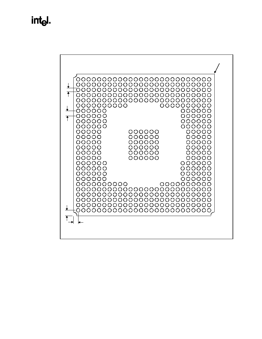
Intel
Æ
82443MX100 PCIset
Datasheet
143
Figure 31. 440MX BGA Package Dimensions (Bottom View)
492_pkg2.vsd
A
B
C
D
E
F
G
H
J
K
L
P
R
T
U
V
Y
AB
AA
AC
2
10
16
20
22
3
5
7
9
11
13
15
17
19
1
21
23
AD
AE
N
25 24
W
4
6
18
8
12
14
M
AF
26
Pin A1 corner
b
e
j
l
492 BGA
Bottom View

Intel
Æ
82443MX100 PCIset
144
Datasheet
Table 80. 440MX Package Dimensions
Symbol
E = 1.27 mm (solder ball pitch)
Notes
Min (mm)
Nominal (mm)
Max (mm)
A
2.17
2.38
2.59
A1
0.50
0.60
0.70
A2
1.12
1.17
1.22
B
0.60
0.75
0.90
C
0.55
0.61
0.67
D
34.80
35.00
35.20
D1
29.75
30.00
30.25
E
34.80
35.00
35.20
E1
29.75
30.00
30.25
I
1.63 REF.
J
1.63 REF.
M
26 x 26 Matrix
N
4.92

Intel
Æ
82443MX100 PCIset
Datasheet
145
Table 81. Alphabetical BGA Pin List
Signal Name
Pin
Signal Name
Pin
Signal Name
Pin
A20GATE
C4
AD20
B14
CPURST#
J26
A20M#
B4
AD21
C12
CPUSTP#
D3
AC_BIT_CLK
C1
AD22
E13
CS0#
AF19
AC_SDATA_IN0
D2
AD23
D12
CS1#
AE17
AC_SDATA_IN1
E1
AD24
C11
CS2#
AD19
AC_RST#
F2
AD25
A16
CS3#
AC16
AC_SDATA_OUT
G5
AD26
B15
DACK0#
AA4
AC_SYNC
D1
AD27
C13
DACK1#
Y5
AD0
D7
AD28
A17
DACK2#
AB1
AD1
A5
AD29
B16
DACK3# / GPIO28
P4
AD2
B8
AD30
B13
DBSY#
U21
AD3
E7
AD31
C15
DCLK
AB25
AD4
B7
ADS#
V26
DCLKO
AC24
AD5
A9
BIOSCS#
R4
DEFER#
R22
AD6
A6
BNR#
R26
DEVSEL#
E8
AD7
A7
BPRI#
R24
DQM0
AD16
AD8
A8
BREQ0#
W25
DQM1
AF16
AD9
B9
BATLOW# /
GPIO11
H3
DQM2
AD25
AD10
C8
C/BE0#
B6
DQM3
AC25
AD11
D10
C/BE1#
B10
DQM4
AE15
AD12
E9
C/BE2#
A13
DQM5
AF17
AD13
A11
C/BE3#
D13
DQM6
AD26
AD14
A10
CKE0#
AA18
DQM7
AC26
AD15
B11
CKE1#
AB17
DRDY#
U22
AD16
C9
CKE2#
AB19
DREQ0
AE4
AD17
D11
CKE3#
AC20
DREQ1
V1
AD18
E10
CLK48
N1
DREQ2
U4
AD19
C10
CLKRUN#
B17
DREQ3/GPIO27
P5
EXSMI#/GPIO24
E2
HA18#
J21
HD14#
F26
FERR#
B1
HA19#
N25
HD15#
H25
FRAME#
A12
HA20#
K23
HD16#
B25
GNTA# / GPIO3
C5
HA21#
L23
HD17#
F24
GPIO1
F4
HA22#
M25
HD18#
D25
GPIO4
J5
HA23#
K22
HD19#
D26
GPIO5
AF4
HA24#
L25
HD20#
D23
GPIO9
J6
HA25#
M26
HD21#
C24

Intel
Æ
82443MX100 PCIset
146
Datasheet
Signal Name
Pin
Signal Name
Pin
Signal Name
Pin
GPIO13
R3
HA26#
J23
HD22#
G22
GPIO15
N5
HA27#
H23
HD23#
H22
GPIO17
K4
HA28#
N23
HD24#
B24
GPIO18
G4
HA29#
L24
HD25#
E22
GPIO20
K3
HA30#
K26
HD26#
C26
GTLREF
F22
HA31#
K25
HD27#
C23
HA3#
P25
HCLKIN
J24
HD28#
A23
HA4#
R23
HD0#
G24
HD29#
A25
HA5#
N22
HD1#
G26
HD30#
E23
HA6#
R25
HD2#
E26
HD31#
B26
HA7#
P22
HD3#
D24
HD32#
E21
HA8#
N24
HD4#
H26
HD33#
B23
HA9#
T25
HD5#
F25
HD34#
C21
HA10#
P23
HD6#
J25
HD35#
A24
HA11#
M24
HD7#
E25
HD36#
B22
HA12#
M23
HD8#
H21
HD37#
D21
HA13#
M22
HD9#
J22
HD38#
F19
HA14#
P26
HD10#
G25
HD39#
D22
HA15#
N26
HD11#
F23
HD40#
C17
HA16#
L22
HD12#
G23
HD41#
B20
HA17#
L26
HD13#
C25
HD42#
A21
HD43#
B21
IGNNE#
A2
MA12#
AF21
HD44#
D20
INIT#
B2
MA13
AF22
HD45#
D19
INTR
B3
MCCS# / GPIO25
T5
HD46#
E20
IOCHRDY
R1
MD0
AE9
HD47#
F18
IOR#
Y4
MD1
AF9
HD48#
E19
IOW#
U3
MD2
AF10
HD49#
C20
IRDY#
D9
MD3
AE10
HD50#
E16
IRQ1
AD2
MD4
AD9
HD51#
A22
IRQ3
Y3
MD5
AC10
HD52#
C18
IRQ4
AF3
MD6
AE11
HD53#
A20
IRQ5
W6
MD7
AF11
HD54#
E17
IRQ6
Y2
MD8
AF12
HD55#
D18
IRQ7
AE3
MD9
AF13
HD56#
D17
IRQ8# / GPIO6
H5
MD10
AE12
HD57#
B19
IRQ12
AF2
MD11
AD15
HD58#
A19
IRQ14
F5
MD12
AE13
HD59#
E18
KBCCS# /
GPIO26
R5
MD13
AF14

Intel
Æ
82443MX100 PCIset
Datasheet
147
Signal Name
Pin
Signal Name
Pin
Signal Name
Pin
HD60#
B18
LID / GPIO10
H4
MD14
AF15
HD61#
F17
MA0#
AE18
MD15
AE14
HD62#
A18
MA1#
AC17
MD16
AB20
HD63#
D16
MA2#
AC19
MD17
AC21
HIT#
V23
MA3#
AE19
MD18
AB22
HITM#
U26
MA4#
AC18
MD19
AB21
HLOCK#
U23
MA5#
AB18
MD20
Y21
HREQ0#
T26
MA6#
AD20
MD21
AA22
HREQ1#
T23
MA7#
AE20
MD22
AC23
HREQ2#
T22
MA8#
AF20
MD23
AC22
HREQ3#
V25
MA9#
AE21
MD24
AB23
HREQ4#
U25
MA10
AE22
MD25
AA23
HTRDY#
T24
MA11#
AD21
MD26
Y22
MD27
W22
MD57
AA26
PDD6
AB8
MD28
W21
MD58
AA25
PDD7
AA8
MD29
W23
MD59
AB24
PDD8
AB9
MD30
Y23
MD60
Y24
PDD9
AA10
MD31
W24
MD61
Y25
PDD10
AC8
MD32
AC9
MD62
Y26
PDD11
AE7
MD33
AB10
MD63
V22
PDD12
AA9
MD34
AC11
MEMR#
U1
PDD13
AF7
MD35
AB11
MEMW#
U2
PDD14
AE8
MD36
AC12
NMI
A3
PDD15
AC6
MD37
AD11
OC0#
L1
PDDAK#
AB5
MD38
AB12
OC1#
M4
PDDRQ
AF5
MD39
AD13
OSC
AB4
PDIOR#
AF6
MD40
AB14
PAR
B12
PDIOW#
AB7
MD41
AC13
PCICLK
A15
PGNT0#
E15
MD42
AD12
PCIRST#
E12
PGNT1#
C16
MD43
AC14
PCISTP#
E4
PGNT2#
D14
MD44
AB15
PCS0# / GPIO19
N4
PGNT3# / GPIO30
B5
MD45
AB16
PCS1# / GPIO16
P3
PIORDY
AA5
MD46
AC15
PDA0
AF8
PIRQA#
D5
MD47
AD17
PDA1
AA6
PIRQB#
E5
MD48
AE23
PDA2
AD7
PIRQC# / GPIO22
C6
MD49
AE24
PDCS1#
AB6
PIRQD# / GPIO23
E6
MD50
AF23
PDCS3#
AC5
PLOCK#
F8
MD51
AF24
PDD0
AA7
PME# / GPIO0
F1
MD52
AE25
PDD1
AE6
PREQ0#
D15

Intel
Æ
82443MX100 PCIset
148
Datasheet
Signal Name
Pin
Signal Name
Pin
Signal Name
Pin
MD53
AD23
PDD2
AD5
PREQ1#
A14
MD54
AE26
PDD3
AD8
PREQ2#
E14
MD55
AF25
PDD4
AE5
PREQ3# / GPIO29
A4
MD56
AB26
PDD5
AC7
PWRBTN#
H2
PWROK
M2
SA18
U5
USBPRT0+
J1
RCIN#
D4
SCAS#
AF18
USBPRT1-
L2
REFVCC
F7
SD0
V5
USBPRT1+
K2
REQA# / GPIO2
D6
SD1
V2
VCC
C3
RI# / GPIO12
J4
SD2
T2
VCC
AD3
RS0#
W26
SD3
R2
VCC
G6
RS1#
V24
SD4
V6
VCC
Y6
RS2#
V21
SD5
V4
VCC
E11
RSMRST#
M5
SD6
T3
VCC
L11
RSTDRV
T4
SD7
T1
VCC
N11
RTCX1
M1
SERIRQ / GPIO7
F6
VCC
P11
RTCX2
M3
SERR#
D8
VCC
T11
SA0
AC1
SMBCLK
J3
VCC
L13
SA1
AE1
SMBDATA
J2
VCC
T13
SA2
AD1
SMI#
C2
VCC
AB13
SA3
AE2
SPKR / GPIO14
P1
VCC
L14
SA4
AA2
SRAS#
AE16
VCC
T14
SA5
AB2
STOP#
F9
VCC
L16
SA6
AA3
STPCLK#
E3
VCC
N16
SA7
AC4
SUS_STAT#
L3
VCC
P16
SA8
AB3
SUSA#
G3
VCC
T16
SA9
W1
SUSB#
G2
VCC
AA17
SA10
AA1
SUSC#
G1
VCC
G21
SA11
AC2
SUSCLK
H1
VCC
AA21
SA12
W5
SYSCLK
V3
VCC
AD24
SA13
AC3
TC
AD4
VCCRTC
N2
SA14
W2
TEST#
K5
VCCSUS
K6
SA15
Y1
THRM# / GPIO8
H6
VCCUSB
L5
SA16
U6
TRDY#
F10
VSS
C19
SA17
W4
USBPRT0-
L4
VSS
AA20
VSS
A1
VSS
M13
VSS
F21
VSS
AF1
VSS
N13
VSS
C22
VSS
F3
VSS
P13
VSS
AD22
VSS
N3
VSS
R13
VSS
E24
VSS
W3
VSS
C14
VSS
H24

Intel
Æ
82443MX100 PCIset
Datasheet
149
Signal Name
Pin
Signal Name
Pin
Signal Name
Pin
VSS
AD6
VSS
M14
VSS
K24
VSS
C7
VSS
P12
VSS
P14
VSS
AD10
VSS
R12
VSS
R14
VSS
M11
VSS
T12
VSS
P24
VSS
R11
VSS
N14
VSS
U24
VSS
L12
VSS
AD14
VSS
AA24
VSS
M12
VSS
L15
VSS
A26
VSS
N12
VSS
M15
VSS
AF26
VSS
N15
VSS
M16
VTTA
K21
VSS
P15
VSS
R16
VTTB
F20
VSS
R15
VSS
AD18
WE#
AA19
VSS
T15
VSSUSB
K1
ZEROWS# /
GPIO21
P2

Intel
Æ
82443MX100 PCIset
150
Datasheet
Table 82. GPIO Pin List
Signal Name
Pin
Signal Name
Pin
Signal Name
Pin
GPIO0 / PME#
F1
GPIO11 / BATLOW#
H3
GPIO22 / PIRQC#
C6
GPIO1
F4
GPIO12 / RI#
J4
GPIO23 / PIRQD#
E6
GPIO2 / REQA#
D6
GPIO13
R3
GPIO24 / EXSMI#
E2
GPIO3 / GNTA#
C5
GPIO14 / SPKR
P1
GPIO25 / MCCS#
T5
GPIO4
J5
GPIO15
N5
GPIO26 / KBCCS#
R5
GPIO5
AF4
GPIO16 / PCS1#
P3
GPIO27 / DREQ3
P5
GPIO6 / IRQ8#
H5
GPIO17
K4
GPIO28 / DACK3#
P4
GPIO7 / SERIRQ
F6
GPIO18
G4
GPIO29 / PREQ3#
A4
GPIO8 / THRM#
H6
GPIO19 / PCS0#
N4
GPIO30 / PGNT3#
B5
GPIO9
J6
GPIO20
K3
GPIO10 / LID
H4
GPIO21 / ZEROWS#
P2