
December 1994
Order Number 271327-001
SPECIAL ENVIRONMENT 80960CA-25 -16
32-BIT HIGH-PERFORMANCE EMBEDDED PROCESSOR
Two Instructions Clock Sustained Execution
Four 59 Mbytes s DMA Channels with Data Chaining
Demultiplexed 32-bit Burst Bus with Pipelining
Y
32-bit Parallel Architecture
Two Instructions clock Execution
Load Store Architecture
Sixteen 32-bit Global Registers
Sixteen 32-bit Local Registers
Manipulates 64-bit Bit Fields
11 Addressing Modes
Full Parallel Fault Model
Supervisor Protection Model
Y
Fast Procedure Call Return Model
Full Procedure Call in 4 Clocks
Y
On-Chip Register Cache
Caches Registers on Call Ret
Minimum of 6 Frames Provided
Up to 15 Programmable Frames
Y
On-Chip instruction Cache
1 Kbyte Two-Way Set Associative
128-bit Path to instruction Sequencer
Cache-Lock Modes
Cache-Off Mode
Y
High Bandwidth On-Chip Data RAM
1 Kbyte On-Chip Data RAM
Sustains 128 bits per Clock Access
Y
Four On-Chip DMA Channels
59 Mbytes s Fly-by Transfers
32 Mbytes s Two-Cycle Transfers
Data Chaining
Data Packing Unpacking
Programmable Priority Method
Y
32-Bit Demultiplexed Burst Bus
128-bit internal Data Paths to
and
from Registers
Burst Bus for DRAM Interfacing
Address Pipelining Option
Fully Programmable Wait States
Supports 8- 16- or 32-bit Bus Widths
Supports Unaligned Accesses
Supervisor Protection Pin
Y
Selectable Big or Little Endian Byte
Ordering
Y
High-Speed Interrupt Controller
Up to 248 External interrupts
32 Fully Programmable Priorities
Multi-mode 8-bit Interrupt Port
Four internal DMA Interrupts
Separate Non-maskable interrupt Pin
Context Switch in 750 ns Typical
Y
Product Grades Available
SE3
b
40 C to
a
110 C

SPECIAL ENVIRONMENT 80960CA-25 -16
32-BIT HIGH-PERFORMANCE EMBEDDED PROCESSOR
CONTENTS
PAGE
1 0 PURPOSE
5
2 0 80960CA OVERVIEW
5
2 1 The C-Series Core
6
2 2 Pipelined Burst Bus
6
2 3 Flexible DMA Controller
6
2 4 Priority Interrupt Controller
6
2 5 Instruction Set Summary
7
3 0 PACKAGE INFORMATION
8
3 1 Package Introduction
8
3 2 Pin Descriptions
8
3 3 80960CA Mechanical Data
15
3 3 1 80960CA PGA Pinout
15
3 4 Package Thermal Specifications
19
3 5 Stepping Register Information
21
3 6 Suggested Sources for 80960CA Accessories
21
4 0 ELECTRICAL SPECIFICATIONS
22
4 1 Absolute Maximum Ratings
22
4 2 Operating Conditions
22
4 3 Recommended Connections
22
4 4 DC Specifications
23
4 5 AC Specifications
24
4 5 1 AC Test Conditions
28
4 5 2 AC Timing Waveforms
28
4 5 3 Derating Curves
32
5 0 RESET BACKOFF AND HOLD ACKNOWLEDGE
34
6 0 BUS WAVEFORMS
35
7 0 REVISION HISTORY
62
2

CONTENTS
PAGE
LIST OF FIGURES
Figure 1
80960CA Block Diagram
5
Figure 2
80960CA PGA Pinout
View from Top (Pins Facing Down)
17
Figure 3
80960CA PGA Pinout
View from Bottom (Pins Facing Up)
18
Figure 4
Measuring 80960CA PGA Case Temperature
19
Figure 5
Register g0
21
Figure 6
AC Test Load
28
Figure 7
Input and Output Clocks Waveform
28
Figure 8
CLKIN Waveform
28
Figure 9
Output Delay and Float Waveform
29
Figure 10 Input Setup and Hold Waveform
29
Figure 11 NMI XINT7 0 Input Setup and Hold Waveform
30
Figure 12 Hold Acknowledge Timings
30
Figure 13 Bus Backoff (BOFF) Timings
31
Figure 14 Relative Timings Waveforms
32
Figure 15 Output Delay or Hold vs Load Capacitance
32
Figure 16 Rise and Fall Time Derating at Highest Operating Temperature
and Minimum V
CC
33
Figure 17 I
CC
vs Frequency and Temperature
33
Figure 18 Cold Reset Waveform
35
Figure 19 Warm Reset Waveform
36
Figure 20 Entering the ONCE State
37
Figure 21 Clock Synchronization in the 2-x Clock Mode
38
Figure 22 Clock Synchronization in the 1-x Clock Mode
38
Figure 23 Non-Burst Non-Pipelined Requests without Wait States
39
Figure 24 Non-Burst Non-Pipelined Read Request with Wait States
40
Figure 25 Non-Burst Non-Pipelined Write Request with Wait States
41
Figure 26 Burst Non-Pipelined Read Request without Wait States 32-Bit Bus
42
Figure 27 Burst Non-Pipelined Read Request with Wait States 32-Bit Bus
43
Figure 28 Burst Non-Pipelined Write Request without Wait States 32-Bit Bus
44
Figure 29 Burst Non-Pipelined Write Request with Wait States 32-Bit Bus
45
Figure 30 Burst Non-Pipelined Read Request with Wait States 16-Bit Bus
46
Figure 31 Burst Non-Pipelined Read Request with Wait States 8-Bit Bus
47
Figure 32 Non-Burst Pipelined Read Request without Wait States 32-Bit Bus
48
Figure 33 Non-Burst Pipelined Read Request with Wait States 32-Bit Bus
49
Figure 34 Burst Pipelined Read Request without Wait States 32-Bit Bus
50
Figure 35 Burst Pipelined Read Request with Wait States 32-Bit Bus
51
Figure 36 Burst Pipelined Read Request with Wait States 16-Bit Bus
52
Figure 37 Burst Pipelined Read Request with Wait States 8-Bit Bus
53
3

CONTENTS
PAGE
LIST OF FIGURES
(Continued)
Figure 38 Using External READY
54
Figure 39 Terminating a Burst with BTERM
55
Figure 40 BOFF Functional Timing
56
Figure 41 HOLD Functional Timing
57
Figure 42 DREQ and DACK Functional Timing
58
Figure 43 EOP Functional Timing
58
Figure 44 Terminal Count Functional Timing
59
Figure 45 FAIL Functional Timing
59
Figure 46 A Summary of Aligned and Unaligned Transfers for Little Endian Regions
60
Figure 47 A Summary of Aligned and Unaligned Transfers for Little Endian Regions
(Continued)
61
Figure 48 Idle Bus Operation
62
LIST OF TABLES
Table 1
80960CA Instruction Set
7
Table 2
Pin Description Nomenclature
8
Table 3
80960CA Pin Description
External Bus Signals
9
Table 4
80960CA Pin Description
Processor Control Signals
12
Table 5
80960CA Pin Description
DMA and Interrupt Unit Control Signals
14
Table 6
80960CA PGA Pinout
In Signal Order
15
Table 7
80960CA PGA Pinout
In Pin Order
16
Table 8
Maximum T
A
at Various Airflows in C
19
Table 9
80960CA PGA Package Thermal Characteristics
20
Table 10 Die Stepping Cross Reference
21
Table 11 Operating Conditions (80960CA-25 -16)
22
Table 12 DC Characteristics
23
Table 13 80960CA AC Characteristics (25 MHz)
24
Table 14 80960CA AC Characteristics (16 MHz)
26
Table 15 Reset Conditions
34
Table 16 Hold Acknowledge and Backoff Conditions
34
4
SPECIAL ENVIRONMENT 80960CA-25 -16
1 0 PURPOSE
This document provides electrical characteristics for
the 25 and 16 MHz versions of the 80960CA For a
detailed description of any 80960CA functional
topic
other than parametric performance
consult
the
80960CA Product Overview
(Order No 270669)
or the
i960
CA Microprocessor User's Manual
(Or-
der No 270710) To obtain data sheet updates and
errata please call Intel's FaxBACK
data-on-de-
mand system (1-800-628-2283 or 916-356-3105)
Other information can be obtained from Intel's tech-
nical BBS (916-356-3600)
2 0 80960CA OVERVIEW
The 80960CA is the second-generation member of
the 80960 family of embedded processors The
80960CA is object code compatible with the 32-bit
80960 Core Architecture while including Special
Function Register extensions to control on-chip pe-
ripherals and instruction set extensions to shift
64-bit operands and configure on-chip hardware
Multiple 128-bit internal buses on-chip instruction
caching and a sophisticated instruction scheduler al-
low the processor to sustain execution of two in-
structions every clock and peak at execution of
three instructions per clock
A 32-bit demultiplexed and pipelined burst bus pro-
vides a 132 Mbyte s bandwidth to a system's high-
speed external memory sub-system In addition the
80960CA's on-chip caching of instructions proce-
dure context and critical program data substantially
decouple system performance from the wait states
associated with accesses to the system's slower
cost sensitive main memory subsystem
The 80960CA bus controller integrates full wait state
and bus width control for highest system perform-
ance with minimal system design complexity Un-
aligned access and Big Endian byte order support
reduces the cost of porting existing applications to
the 80960CA
The processor also integrates four complete data-
chaining DMA channels and a high-speed interrupt
controller on-chip DMA channels perform single-
cycle or two-cycle transfers data packing and un-
packing and data chaining Block transfers
in addi-
tion to source or destination synchronized trans-
fers
are provided
The interrupt controller provides full programmability
of 248 interrupt sources into 32 priority levels with a
typical interrupt task switch (``latency'') time of
750 ns
271327 ≠ 1
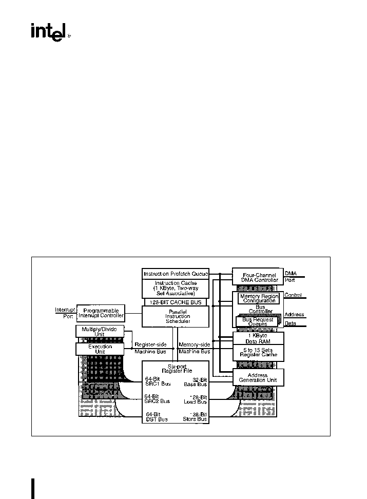
Figure 1 80960CA Block Diagram
5

SPECIAL ENVIRONMENT 80960CA-25 -16
2 1 The C-Series Core
The C-Series core is a very high performance micro-
architectural implementation of the 80960 Core Ar-
chitecture The C-Series core can sustain execution
of two instructions per clock (50 MIPs at 25 MHz)
To achieve this level of performance Intel has incor-
porated state-of-the-art silicon technology and inno-
vative microarchitectural constructs into the imple-
mentation of the C-Series core Factors that contrib-
ute to the core's performance include
Parallel instruction decoding allows issuance of
up to three instructions per clock
Single-clock execution of most instructions
Parallel instruction decode allows sustained
simultaneous execution of two single-clock in-
structions every clock cycle
Efficient instruction pipeline minimizes pipeline
break losses
Register and resource scoreboarding allow simul-
taneous multi-clock instruction execution
Branch look-ahead and prediction allows many
branches to execute with no pipeline break
Local Register Cache integrated on-chip caches
Call Return context
Two-way set associative 1 Kbyte integrated in-
struction cache
1 Kbyte integrated Data RAM sustains a four-
word (128-bit) access every clock cycle
2 2 Pipelined Burst Bus
A 32-bit high performance bus controller interfaces
the 80960CA to external memory and peripherals
The Bus Control Unit features a maximum transfer
rate of 100 Mbytes per second (at 25 MHz) Internal-
ly programmable wait states and 16 separately con-
figurable memory regions allow the processor to in-
terface with a variety of memory subsystems with a
minimum of system complexity and a maximum of
performance The Bus Controller's main features in-
clude
Demultiplexed Burst Bus to exploit most efficient
DRAM access modes
Address Pipelining to reduce memory cost while
maintaining performance
32- 16- and 8-bit modes for I O interfacing ease
Full internal wait state generation to reduce sys-
tem cost
Little and Big Endian support to ease application
development
Unaligned access support for code portability
Three-deep request queue to decouple the bus
from the core
2 3 Flexible DMA Controller
A four-channel DMA controller provides high speed
DMA control for data transfers involving peripherals
and memory The DMA provides advanced features
such as data chaining byte assembly and disassem-
bly and a high performance fly-by mode capable of
transfer speeds of up to 45 Mbytes per second at
25 MHz The DMA controller features a performance
and flexibility which is only possible by integrating
the DMA controller and the 80960CA core
2 4 Priority interrupt Controller
A programmable-priority interrupt controller man-
ages up to 248 external sources through the 8-bit
external interrupt port The interrupt Unit also han-
dles the four internal sources from the DMA control-
ler and a single non-maskable interrupt input The
8-bit interrupt port can also be configured to provide
individual interrupt sources that are level or edge
triggered
Interrupts in the 80960CA are prioritized and sig-
naled within 270 ns of the request If the interrupt is
of higher priority than the processor priority the con-
text switch to the interrupt routine typically is com-
plete in another 480 ns The interrupt unit provides
the mechanism for the low latency and high through-
put interrupt service which is essential for embedded
applications
6

SPECIAL ENVIRONMENT 80960CA-25 -16
2 5 Instruction Set Summary
Table 1 summarizes the 80960CA instruction set by logical groupings See the
i960
CA Microprocessor
User's Manual
for a complete description of the instruction set
Table 1 80960CA Instruction Set
Data
Arithmetic
Logical
Bit and Bit Field
Movement
and Byte
Load
Add
And
Set Bit
Store
Subtract
Not And
Clear Bit
Move
Multiply
And Not
Not Bit
Load Address
Divide
Or
Alter Bit
Remainder
Exclusive Or
Scan For Bit
Modulo
Not Or
Span Over Bit
Shift
Or Not
Extract
Extended Shift
Nor
Modify
Extended Multiply
Exclusive Nor
Scan Byte for Equal
Extended Divide
Not
Add with Carry
Nand
Subtract with Carry
Rotate
Comparison
Branch
Call Return
Fault
Compare
Unconditional Branch
Call
Conditional Fault
Conditional Compare
Conditional Branch
Call Extended
Synchronize Faults
Compare and Increment
Compare and Branch
Call System
Compare and Decrement
Return
Test Condition Code
Branch and Link
Check Bit
Debug
Processor
Atomic
Management
Modify Trace Controls
Flush Local Registers
Atomic Add
Mark
Modify Arithmetic Controls
Atomic Modify
Force Mark
Modify Process Controls
System Control
DMA Control
NOTES
Instructions marked by ( ) are 80960CA extensions to the 80960 instruction set
7

SPECIAL ENVIRONMENT 80960CA-25 -16
3 0 PACKAGE INFORMATION
3 1 Package Introduction
This section describes the pins pinouts and thermal
characteristics for the 80960CA in the 168-pin Ce-
ramic Pin Grid Array (PGA) package For complete
package specifications and information
see the
Packaging
Handbook (Order No 240800)
3 2 Pin Descriptions
The 80960CA pins are described in this section Ta-
ble 2 presents the legend for interpreting the pin de-
scriptions in the following tables Pins associated
with the 32-bit demultiplexed processor bus are de-
scribed in Table 3 Pins associated with basic proc-
essor configuration and control are described in Ta-
ble 4 Pins associated with the 80960CA DMA Con-
troller and Interrupt Unit are described in Table 5
All pins float while the processor is in the ONCE
mode
Table 2 Pin Description Nomenclature
Symbol
Description
I
Input only pin
O
Output only pin
I O
Pin can be either an input or output
Pins ``must be'' connected as described
S( )
Synchronous Inputs must meet setup
and hold times relative to PCLK2 1 for
proper operation All outputs are
synchronous to PCLK2 1
S(E)
Edge sensitive input
S(L)
Level sensitive input
A( )
Asynchronous Inputs may be
asynchronous to PCLK2 1
A(E)
Edge sensitive input
A(L)
Level sensitive input
H( )
While the processor's bus is in the Hold
Acknowledge or Bus Backoff state the
pin
H(1)
is driven to V
CC
H(0)
is driven to V
SS
H(Z)
floats
H(Q) continues to be a valid input
R( )
While the processor's RESET pin is low
the pin
R(1)
is driven to V
CC
R(0)
is driven to V
SS
R(Z)
floats
R(Q) continues to be a valid output
8
SPECIAL ENVIRONMENT 80960CA-25 -16
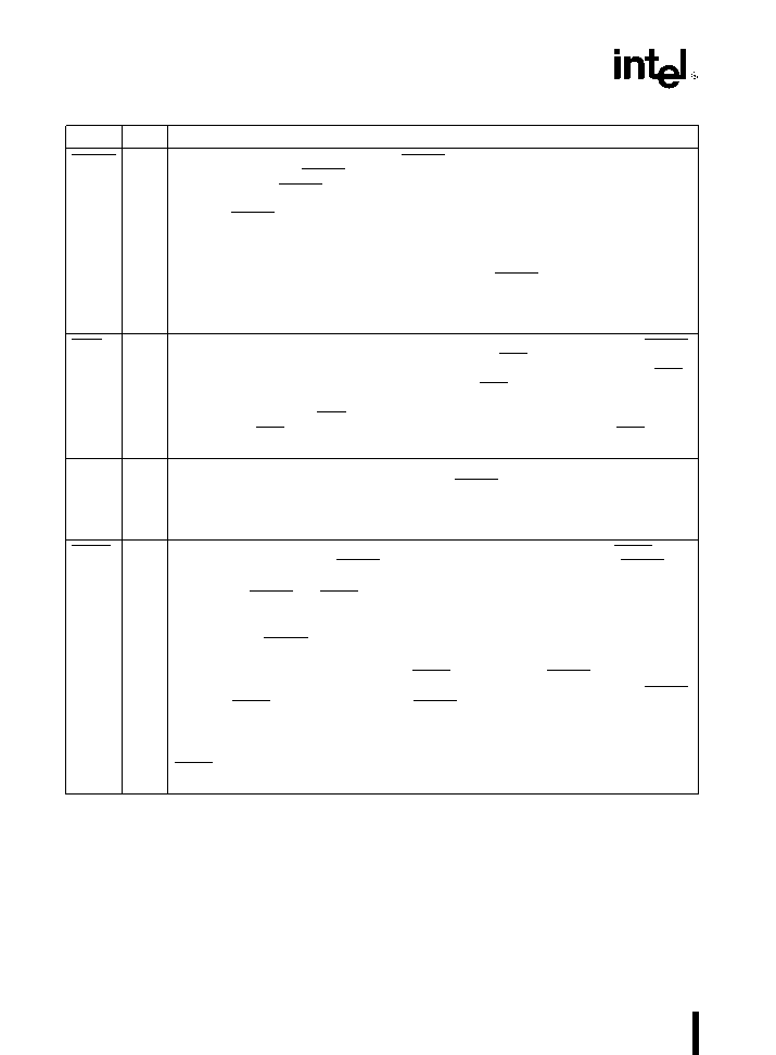
Table 3 80960CA Pin Description
External Bus Signals
Name
Type
Description
A31 2
O
ADDRESS BUS
carries the physical address' upper 30 bits A31 is the most
significant address bit A2 is the least significant During a bus access A31 2
S
identify all external addresses to word (4-byte) boundaries The byte enable signals
H(Z)
indicate the selected byte in each word During burst accesses A3 2 increment to
R(Z)
indicate successive data cycles
D31 0
I O
DATA BUS
carries 32- 16- or 8-bit data quantities depending on bus width
configuration The least significant bit of the data is carried on D0 and the most
S(L)
significant on D31 When the bus is configured for 8-bit data the lower 8 data lines
H(Z)
D7 0 are used For 16-bit data bus widths D15 0 are used For 32 bit bus widths the
R(Z)
full data bus is used
BE3 0
O
BYTE ENABLES
select which of the four bytes addressed by A31 2 are active
during an access to a memory region configured for a 32-bit data-bus width BE3
S
applies to D31 24 BE2 applies to D23 16 BE1 applies to D15 8 BE0 applies to
H(Z)
D7 0
R(1)
32-bit bus
BE3
Byte Enable 3
enable D31 24
BE2
Byte Enable 2
enable D23 16
BE1
Byte Enable 1
enable D15 8
BE0
Byte Enable 0
enable D7 0
For accesses to a memory region configured for a 16-bit data-bus width the
processor uses the BE3 BE1 and BE0 pins as BHE A1 and BLE respectively
16-bit bus
BE3
Byte High Enable (BHE)
enable D15 8
BE2
Not used (driven high or low)
BE1
Address Bit 1 (A1)
BE0
Byte Low Enable (BLE)
enable D7 0
For accesses to a memory region configured for an 8-bit data-bus width the
processor uses the BE1 and BE0 pins as A1 and A0 respectively
8-bit bus
BE3
Not used (driven high or low)
BE2
Not used (driven high or low)
BE1
Address Bit 1 (A1)
BE0
Address Bit 0 (A0)
W R
O
WRITE READ
is asserted for read requests and deasserted for write requests The
W R signal changes in the same clock cycle as ADS It remains valid for the entire
S
access in non-pipelined regions In pipelined regions W R is not guaranteed to be
H(Z)
valid in the last cycle of a read access
R(0)
ADS
O
ADDRESS STROBE
indicates a valid address and the start of a new bus access
ADS is asserted for the first clock of a bus access
S
H(Z)
R(1)
9
SPECIAL ENVIRONMENT 80960CA-25 -16
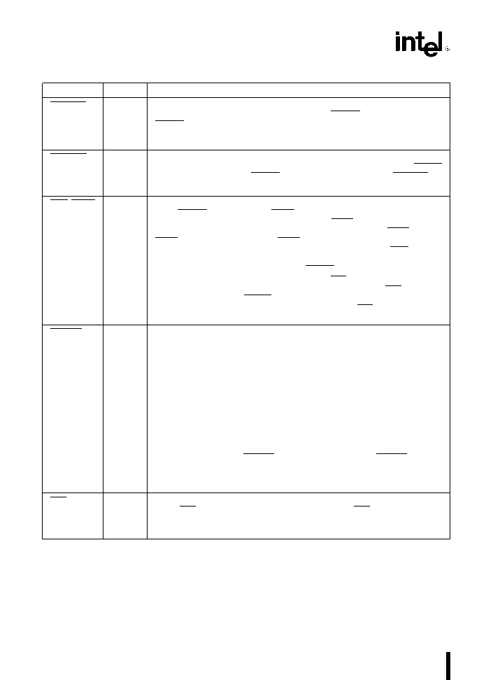
Table 3 80960CA Pin Description
External Bus Signals
(Continued)
Name
Type
Description
READY
I
READY
is an input which signals the termination of a data transfer READY is
used to indicate that read data on the bus is valid or that a write-data transfer
S(L)
has completed The READY signal works in conjunction with the internally
H(Z)
programmed wait-state generator If READY is enabled in a region the pin is
R(Z)
sampled after the programmed number of wait-states has expired If the
READY pin is deasserted wait states continue to be inserted until READY
becomes asserted This is true for the N
RAD
N
RDD
N
WAD
and N
WDD
wait
states The N
XDA
wait states cannot be extended
BTERM
I
BURST TERMINATE
is an input which breaks up a burst access and causes
another address cycle to occur The BTERM signal works in conjunction with
S(L)
the internally programmed wait-state generator If READY and BTERM are
H(Z)
enabled in a region the BTERM pin is sampled after the programmed number
R(Z)
of wait states has expired When BTERM is asserted a new ADS signal is
generated and the access is completed The READY input is ignored when
BTERM is asserted BTERM must be externally synchronized to satisfy
BTERM setup and hold times
WAIT
O
WAIT
indicates internal wait state generator status WAIT is asserted when
wait states are being caused by the internal wait state generator and not by
S
the READY or BTERM inputs WAIT can be used to derive a write-data
H(Z)
strobe WAIT can also be thought of as a READY output that the processor
R(1)
provides when it is inserting wait states
BLAST
O
BURST LAST
indicates the last transfer in a bus access BLAST is asserted
in the last data transfer of burst and non-burst accesses after the wait state
S
counter reaches zero BLAST remains asserted until the clock following the
H(Z)
last cycle of the last data transfer of a bus access If the READY or BTERM
R(0)
input is used to extend wait states the BLAST signal remains asserted until
READY or BTERM terminates the access
DT R
O
DATA TRANSMIT RECEIVE
indicates direction for data transceivers DT R
is used in conjunction with DEN to provide control for data transceivers
S
attached to the external bus When DT R is asserted the signal indicates that
H(Z)
the processor receives data Conversely when deasserted the processor
R(0)
sends data DT R changes only while DEN is high
DEN
O
DATA ENABLE
indicates data cycles in a bus request DEN is asserted at the
start of the bus request first data cycle and is deasserted at the end of the last
S
data cycle DEN is used in conjunction with DT R to provide control for data
H(Z)
transceivers attached to the external bus DEN remains asserted for
R(1)
sequential reads from pipelined memory regions DEN is deasserted when
DT R changes
LOCK
O
BUS LOCK
indicates that an atomic read-modify-write operation is in
progress LOCK may be used to prevent external agents from accessing
S
memory which is currently involved in an atomic operation LOCK is asserted
H(Z)
in the first clock of an atomic operation and deasserted in the clock cycle
R(1)
following the last bus access for the atomic operation To allow the most
flexibility for memory system enforcement of locked accesses the processor
acknowledges a bus hold request when LOCK is asserted The processor
performs DMA transfers while LOCK is active
HOLD
I
HOLD REQUEST
signals that an external agent requests access to the
external bus The processor asserts HOLDA after completing the current bus
S(L)
request HOLD HOLDA and BREQ are used together to arbitrate access to
H(Z)
the processor's external bus by external bus agents
R(Z)
10
SPECIAL ENVIRONMENT 80960CA-25 -16
Table 3 80960CA Pin Description
External Bus Signals
(Continued)
Name
Type
Description
BOFF
I
BUS BACKOFF
when asserted suspends the current access and causes
the bus pins to float When BOFF is deasserted the ADS signal is asserted
S(L)
on the next clock cycle and the access is resumed
H(Z)
R(Z)
HOLDA
O
HOLD ACKNOWLEDGE
indicates to a bus requestor that the processor has
relinquished control of the external bus When HOLDA is asserted the
S
external address bus data bus and bus control signals are floated HOLD
H(1)
BOFF HOLDA and BREQ are used together to arbitrate access to the
R(Q)
processor's external bus by external bus agents Since the processor grants
HOLD requests and enters the Hold Acknowledge state even while RESET is
asserted the state of the HOLDA pin is independent of the RESET pin
BREQ
O
BUS REQUEST
is asserted when the bus controller has a request pending
BREQ can be used by external bus arbitration logic in conjunction with HOLD
S
and HOLDA to determine when to return mastership of the external bus to the
H(Q)
processor
R(0)
D C
O
DATA OR CODE
is asserted for a data request and deasserted for instruction
requests D C has the same timing as W R
S
H(Z)
R(Z)
DMA
O
DMA ACCESS
indicates whether the bus request was initiated by the DMA
controller DMA is asserted for any DMA request DMA is deasserted for all
S
other requests
H(Z)
R(Z)
SUP
O
SUPERVISOR ACCESS
indicates whether the bus request is issued while in
supervisor mode SUP is asserted when the request has supervisor privileges
S
and is deasserted otherwise SUP can be used to isolate supervisor code and
H(Z)
data structures from non-supervisor requests
R(Z)
11
SPECIAL ENVIRONMENT 80960CA-25 -16
Table 4 80960CA Pin Description
Processor Control Signals
Name
Type
Description
RESET
I
RESET
causes the chip to reset When RESET is asserted all external signals return to
the reset state When RESET is deasserted initialization begins When the 2-x clock
A(L)
mode is selected RESET must remain asserted for 32 CLKIN cycles before being
H(Z)
deasserted to guarantee correct processor initialization When the 1-x clock mode is
R(Z)
selected RESET must remain asserted for 10 000 CLKIN cycles before being deasserted
to guarantee correct processor initialization The CLKMODE pin selects 1-x or 2-x input
clock division of the CLKIN pin
The processor's Hold Acknowledge bus state functions while the chip is reset If the
processor's bus is in the Hold Acknowledge state when RESET is asserted the processor
will internally reset but maintains the Hold Acknowledge state on external pins until the
Hold request is removed If a Hold request is made while the processor is in the reset
state the processor bus will grant HOLDA and enter the Hold Acknowledge state
FAIL
O
FAIL
indicates failure of the processor's self-test performed at initialization When RESET
is deasserted and the processor begins initialization the FAIL pin is asserted An internal
S
self-test is performed as part of the initialization process If this self-test passes the FAIL
H(Q)
pin is deasserted otherwise it remains asserted The FAIL pin is reasserted while the
R(0)
processor performs an external bus self-confidence test If this self-test passes the
processor deasserts the FAIL pin and branches to the user's initialization routine
otherwise the FAIL pin remains asserted Internal self-test and the use of the FAIL pin can
be disabled with the STEST pin
STEST
I
SELF TEST
causes the processor's internal self-test feature to be enabled or disabled at
initialization STEST is read on the rising edge of RESET When asserted the processor's
S(L)
internal self-test and external bus confidence tests are performed during processor
H(Z)
initialization When deasserted only the bus confidence tests are performed during
R(Z)
initialization
ONCE
I
ON CIRCUIT EMULATION
when asserted causes all outputs to be floated ONCE is
continuously sampled while RESET is low and is latched on the rising edge of RESET To
A(L)
place the processor in the ONCE state
H(Z)
(1) assert RESET and ONCE (order does not matter)
R(Z)
(2) wait for at least 16 CLKIN periods in 2-x mode
or 10 000 CLKIN periods in 1-x
mode
after V
CC
and CLKIN are within operating specifications
(3) deassert RESET
(4) wait at least 32 CLKIN periods
(The processor will now be latched in the ONCE state as long as RESET is high )
To exit the ONCE state bring V
CC
and CLKIN to operating conditions then assert RESET
and bring ONCE high prior to deasserting RESET
CLKIN must operate within the specified operating conditions of the processor until Step 4
above has been completed CLKIN may then be changed to DC to achieve the lowest
possible ONCE mode leakage current
ONCE can be used by emulator products or for board testers to effectively make an
installed processor transparent in the board
12

SPECIAL ENVIRONMENT 80960CA-25 -16
Table 4 80960CA Pin Description
Processor Control Signals
(Continued)
Name
Type
Description
CLKIN
I
CLOCK INPUT
is an input for the external clock needed to run the processor The
external clock is internally divided as prescribed by the CLKMODE pin to produce
A(E)
PCLK2 1
H(Z)
R(Z)
CLKMODE
I
CLOCK MODE
selects the division factor applied to the external clock input (CLKIN)
When CLKMODE is high CLKIN is divided by one to create PCLK2 1 and the
A(L)
processor's internal clock When CLKMODE is low CLKIN is divided by two to create
H(Z)
PCLK2 1 and the processor's internal clock CLKMODE should be tied high or low in a
R(Z)
system as the clock mode is not latched by the processor If left unconnected the
processor will internally pull the CLKMODE pin low enabling the 2-x clock mode
PCLK2 1
O
PROCESSOR OUTPUT CLOCKS
provide a timing reference for all processor inputs
and outputs All input and output timings are specified in relation to PCLK2 and
S
PCLK1 PCLK2 and PCLK1 are identical signals Two output pins are provided to allow
H(Q)
flexibility in the system's allocation of capacitive loading on the clock PCLK2 1 may
R(Q)
also be connected at the processor to form a single clock signal
V
SS
GROUND
connections must be connected externally to a V
SS
board plane
V
CC
POWER
connections must be connected externally to a V
CC
board pane
V
CCPLL
V
CCPLL
is a separate V
CC
supply pin for the phase lock loop used in 1-x clock mode
Connecting a simple lowpass filter to V
CCPLL
may help reduce clock jitter (T
CP
) in
noisy environments Otherwise V
CCPLL
should be connected to V
CC
This pin is
implemented starting with the D-stepping See Table 13 for die stepping information
NC
NO CONNECT
pins must not be connected in a system
13
SPECIAL ENVIRONMENT 80960CA-25 -16
Table 5 80960CA Pin Description
DMA and Interrupt Unit Control Signals
Name
Type
Description
DREQ3 0
I
DMA REQUEST
causes a DMA transfer to be requested Each of the four
signals requests a transfer on a single channel DREQ0 requests channel 0
A(L)
DREQ1 requests channel 1 etc When two or more channels are requested
H(Z)
simultaneously the channel with the highest priority is serviced first The
R(Z)
channel priority mode is programmable
DACK3 0
O
DMA ACKNOWLEDGE
indicates that a DMA transfer is being executed
Each of the four signals acknowledges a transfer for a single channel DACK0
S
acknowledges channel 0 DACK1 acknowledges channel 1 etc DACK3 0 are
H(1)
asserted when the requesting device of a DMA is accessed
R(1)
EOP TC3 0
I O
END OF PROCESS TERMINAL COUNT
can be programmed as either an
input (EOP3 0) or as an output (TC3 0) but not both Each pin is individually
A(L)
programmable When programmed as an input EOPx causes the termination
H(Z Q)
of a current DMA transfer for the channel corresponding to the EOPx pin
R(Z)
EOP0 corresponds to channel 0 EOP1 corresponds to channel 1 etc When
a channel is configured for source
and
destination chaining the EOP pin for
that channel causes termination of only the current buffer transferred and
causes the next buffer to be transferred EOP3 0 are asynchronous inputs
When programmed as an output the channel's TCx pin indicates that the
channel byte count has reached 0 and a DMA has terminated TCx is driven
with the same timing as DACKx during the last DMA transfer for a buffer If the
last bus request is executed as multiple bus accesses TCx will stay asserted
for the entire bus request
XINT7 0
I
EXTERNAL INTERRUPT PINS
cause interrupts to be requested These pins
can be configured in three modes
A(E L)
Dedicated Mode
each pin is a dedicated external interrupt source
H(Z)
Dedicated inputs can be individually programmed to
R(Z)
be level (low) or edge (falling) activated
Expanded Mode
the eight pins act together as an 8-bit vectored
interrupt source The interrupt pins in this mode are
level activated Since the interrupt pins are active low
the vector number requested is the one's
complement of the positive logic value place on the
port This eliminates glue logic to interface to
combinational priority encoders which output
negative logic
Mixed Mode
XINT7 5 are dedicated sources and XINT4 0 act as
the five most significant bits of an expanded mode
vector The least significant bits are set to 010
internally
NMI
I
NON-MASKABLE INTERRUPT
causes a non-maskable interrupt event to
occur NMI is the highest priority interrupt recognized NMI is an edge (falling)
A(E)
activated source
H(Z)
R(Z)
14
SPECIAL ENVIRONMENT 80960CA-25 -16
3 3 80960CA Mechanical Data
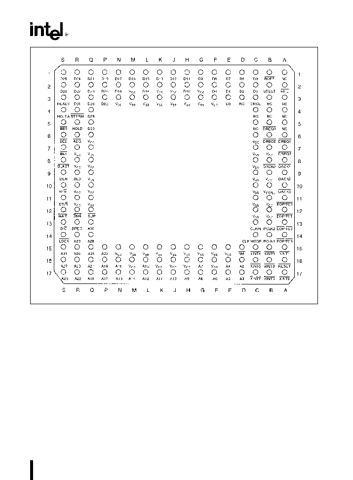
3 3 1 80960CA PGA Pinout
Tables 6 and 7 list the 80960CA pin names with
package location Figure 2 depicts the complete
80960CA PGA pinout as viewed from the top side of
the component (i e
pins facing down) Figure 3
shows the complete 80960CA PGA pinout as
viewed from the pin-side of the package (i e
pins
facing up) See Section 4 0 ELECTRICAL SPECI-
FICATIONS
for specifications and recommended
connections
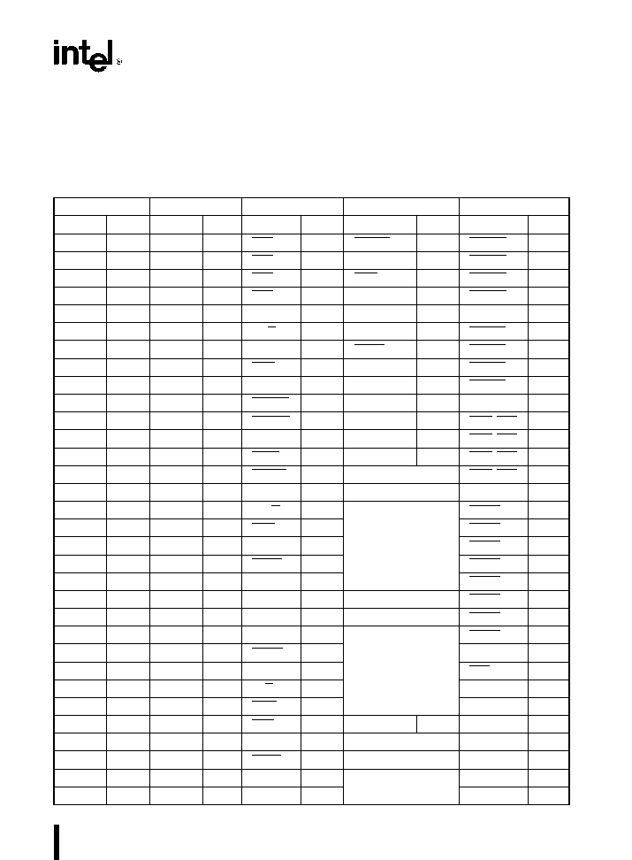
Table 6 80960CA PGA Pinout
In Signal Order
Address Bus
Data Bus
Bus Control
Processor Control
I O
Signal
Pin
Signal
Pin
Signal
Pin
Signal
Pin
Signal
Pin
A31
S15
D31
R3
BE3
S5
RESET
A16
DREQ3
A7
A30
Q13
D30
Q5
BE2
S6
DREQ2
B6
A29
R14
D29
S2
BE1
S7
FAIL
A2
DREQ1
A6
A28
Q14
D28
Q4
BE0
R9
DREQ0
B5
A27
S16
D27
R2
STEST
B2
A26
R15
D26
Q3
W R
S10
DACK3
A10
A25
S17
D25
S1
ONCE
C3
DACK2
A9
A24
Q15
D24
R1
ADS
R6
DACK1
A8
A23
R16
D23
Q2
CLKIN
C13
DACK0
B8
A22
R17
D22
P3
READY
S3
CLKMODE
C14
A21
Q16
D21
Q1
BTERM
R4
PLCK1
B14
EOP TC3
A14
A20
P15
D20
P2
PLCK2
B13
EOP TC2
A13
A19
P16
D19
P1
WAIT
S12
EOP TC1
A12
A18
Q17
D18
N2
BLAST
S8
V
SS
EOP TC0
A11
A17
P17
D17
N1
Location
A16
N16
D16
M1
DT R
S11
Q8 Q9 Q10 Q11
L15 M3 M15 Q7
J15 K3 K15 L3
G15 H3 H15 J3
C11 C12 F15 G3
C7 C8 C9 C10
XINT7
C17
A15
N17
D15
L1
DEN
S9
XINT6
C16
A14
M17
D14
L2
XINT5
B17
A13
L16
D13
K1
LOCK
S14
XINT4
C15
A12
L17
D12
J1
XINT3
B16
A11
K17
D11
H1
V
CC
XINT2
A17
A10
J17
D10
H2
HOLD
R5
Location
XINT1
A15
A9
H17
D9
G1
HOLDA
S4
R8 R10 R11
N3 N15 Q6 R7
K2 K16 M2 M16
G2 H16 J2 J16
C6 E15 F3 F16
B7 B9 B11 B12
XINT0
B15
A8
G17
D8
F1
BREQ
R13
A7
G16
D7
E1
NMI
D15
A6
F17
D6
F2
D C
S13
A5
E17
D5
D1
DMA
R12
A4
E16
D4
E2
SUP
Q12
V
CCPLL
B10
A3
D17
D3
C1
No Connect
A2
D16
D2
D2
BOFF
B1
Location
D1
C2
B4 C4 C5 D3
A1 A3 A4 A5 B3
D0
E3
15
SPECIAL ENVIRONMENT 80960CA-25 -16
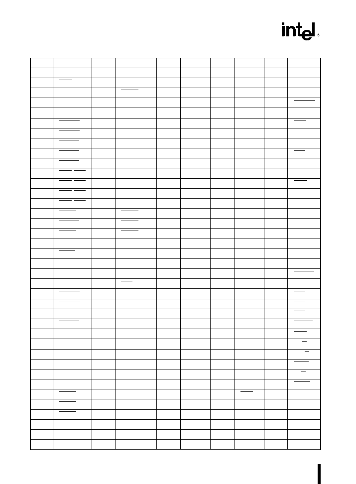
Table 7 80960CA PGA Pinout
In Pin Order
Pin
Signal
Pin
Signal
Pin
Signal
Pin
Signal
Pin
Signal
A1
NC
C1
D3
G1
D9
M1
D16
R1
D24
A2
FAIL
C2
D1
G2
V
CC
M2
V
CC
R2
D27
A3
NC
C3
ONCE
G3
V
SS
M3
V
SS
R3
D31
A4
NC
C4
NC
G15
V
SS
M15
V
SS
R4
BTERM
A5
NC
C5
NC
G16
A7
M16
V
CC
R5
HOLD
A6
DREQ1
C6
V
CC
G17
A8
M17
A14
R6
ADS
A7
DREQ3
C7
V
SS
R7
V
CC
A8
DACK1
C8
V
SS
H1
D11
N1
D17
R8
V
CC
A9
DACK2
C9
V
SS
H2
D10
N2
D18
R9
BE0
A10
DACK3
C10
V
SS
H3
V
SS
N3
V
CC
R10
V
CC
A11
EOP TC0
C11
V
SS
H15
V
SS
N15
V
CC
R11
V
CC
A12
EOP TC1
C12
V
SS
H16
V
CC
N16
A16
R12
DMA
A13
EOP TC2
C13
CLKIN
H17
A9
N17
A15
R13
BREQ
A14
EOP TC3
C14
CLKMODE
R14
A29
A15
XINT1
C15
XINT4
J1
D12
P1
D19
R15
A26
A16
RESET
C16
XINT6
J2
V
CC
P2
D20
R16
A23
A17
XINT2
C17
XINT7
J3
V
SS
P3
D22
R17
A22
J15
V
SS
P15
A20
B1
BOFF
D1
D5
J16
V
CC
P16
A19
S1
D25
B2
STEST
D2
D2
J17
A10
P17
A17
S2
D29
B3
NC
D3
NC
S3
READY
B4
NC
D15
NMI
K1
D13
Q1
D21
S4
HOLDA
B5
DREQ0
D16
A2
K2
V
CC
Q2
D23
S5
BE3
B6
DREQ2
D17
A3
K3
V
SS
Q3
D26
56
BE2
B7
V
CC
K15
V
SS
Q4
Q28
S7
BE1
B8
DACK0
E1
D7
K16
V
CC
Q5
D30
S8
BLAST
B9
V
CC
E2
D4
K17
A11
Q6
V
CC
S9
DEN
B10
V
CCPLL
E3
D0
Q7
V
SS
S10
W R
B11
V
CC
E15
V
CC
L1
D15
Q8
V
SS
S11
DT R
B12
V
CC
E16
A4
L2
D14
Q9
V
SS
S12
WAIT
B13
PCLK2
E17
A5
L3
V
SS
Q10
V
SS
S13
D C
B14
PCLK1
L15
V
SS
Q11
V
SS
S14
LOCK
B15
XINT0
F1
D8
L16
A13
Q12
SUP
S15
A31
B16
XINT3
F2
D6
L17
A12
Q13
A30
S16
A27
B17
XINT5
F3
V
CC
Q14
A28
S17
A25
F15
V
SS
Q15
A24
F16
V
CC
Q16
A21
F17
A6
Q17
A18
16
SPECIAL ENVIRONMENT 80960CA-25 -16
271327 ≠ 2
Figure 2 80960CA PGA Pinout
View from Top (Pins Facing Down)
17
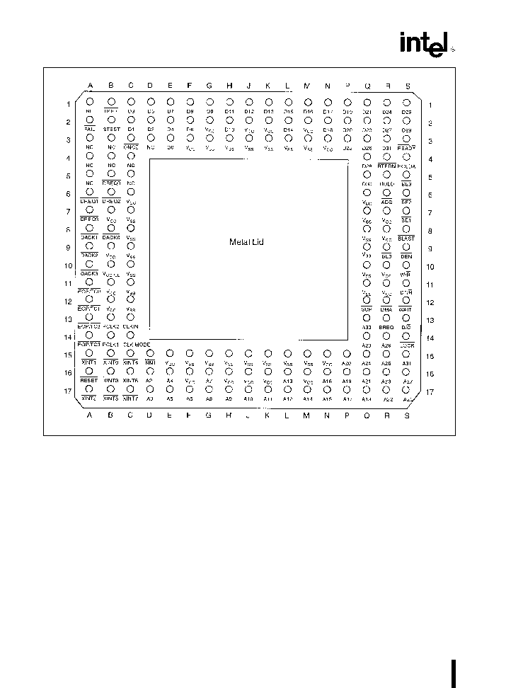
SPECIAL ENVIRONMENT 80960CA-25 -16
271327 ≠ 3
Figure 3 80960CA PGA Pinout
View from Bottom (Pins Facing Up)
18
SPECIAL ENVIRONMENT 80960CA-25 -16
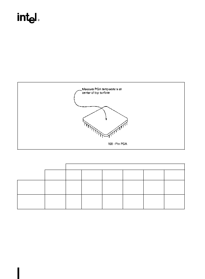
3 4 Package Thermal Specifications
The 80960CA is specified for operation when T
C
(case temperature) is within the range of b40 C ≠
a
110 C T
C
may be measured in any environment
to determine whether the 80960CA is within speci-
fied operating range Case temperature should be
measured at the center of the top surface opposite
the pins Refer to Figure 4
T
A
(ambient temperature) can be calculated from
i
CA
(thermal resistance from case to ambient) using
the following equation
T
A
e
T
C
b
P i
CA
Table 8 shows the maximum T
A
allowable (without
exceeding T
C
) at various airflows and operating fre-
quencies (f
PCLK
)
Note that T
A
is greatly improved by attaching fins or
a heatsink to the package P (maximum power con-
sumption) is calculated by using the typical I
CC
as
tabulated in Section 4 4 DC Specifications and
V
CC
of 5V
271327 ≠ 4
Figure 4 Measuring 80960CA PGA Case Temperature
Table 8 Maximum T
A
at Various Airflows in C
Airflow-ft min (m sec)
f
PCLK
0
200
400
600
800
1000
(MHz)
(0)
(1 01)
(2 03)
(3 04)
(4 06)
(5 07)
T
A
with
33
51
66
79
81
85
87
Heatsink
25
61
73
83
85
88
89
16
74
82
89
90
92
93
T
A
without
33
36
47
59
66
73
75
Heatsink
25
49
58
67
73
78
80
16
66
72
78
82
86
87
NOTES
0 285
high undirectional heatsink (Al alloy 6061 50 mil fin width 150 mil center-to-center fin spacing)
19
SPECIAL ENVIRONMENT 80960CA-25 -16
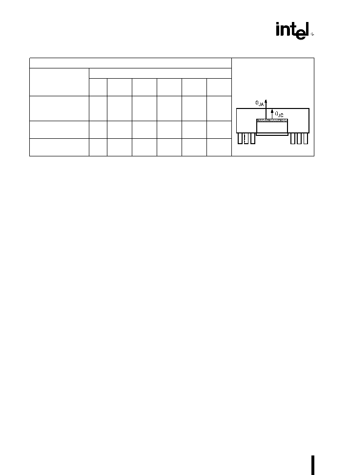
Table 9 80960CA PGA Package Thermal Characteristics
Thermal Resistance
C Watt
Parameter
Airflow
ft min (m sec)
0
200
400
600
800
1000
(0)
(1 01)
(2 03)
(3 07)
(4 06)
(5 07)
i
Junction-to-Case
(Case measured as
1 5
1 5
1 5
1 5
1 5
1 5
shown in Figure 4)
i
Case-to-Ambient
17
14
11
9
7 1
6 6
(No Heatsink)
i
Case-to-Ambient
13
9
5 5
5
3 9
3 4
(With Heatsink)
NOTES
1 This table applies to 80960CA PGA plugged into socket or soldered directly to board
2 i
JA
e
i
JC
a
i
CA
0 285
high unidirectional heatsink (Al alloy 6061 50 mil fin width 150 mil center-to-center fin spacing)
20
SPECIAL ENVIRONMENT 80960CA-25 -16
3 5 Stepping Register Information
Upon reset register g0 contains die stepping infor-
mation Figure 5 shows how g0 is configured The
most significant byte contains an ASCII 0 The upper
middle byte contains an ASCII C The lower middle
byte contains an ASCII A The least significant byte
contains the stepping number in ASCII g0 retains
this information until it is overwritten by the user pro-
gram
ASCII
00
43
41
Stepping Number
DECIMAL
0
C
A
Stepping Number
MSB
LSB
Figure 5 Register g0
Table 10 contains a cross reference of the number
in the least significant byte of register g0 to the die
stepping number
Table 10 Die Stepping Cross Reference
g0 Least Significant
Die Stepping
Byte
01
B
02
C-1
03
C-2 C-3
04
D
3 6 Suggested Sources for 80960CA
Accessories
The following is a list of suggested sources for
80960CA accessories This is not an endorsement
of any kind nor is it a warranty of the performance of
any of the listed products and or companies
Sockets
1 3M Textool Test and Interconnection
Products Department
P O Box 2963
Austin TX 78769-2963
2 Augat Inc
Interconnection Products Group
33 Perry Avenue
P O Box 779
Attleboro MA 02703
(508) 699-7646
3 Concept Manufacturing Inc
(Decoupling Sockets)
41484 Christy Street
Fremont CA 94538
(415) 651-3804
Heatsinks Fins
1 Thermalloy Inc
2021 West Valley View Lane
Dallas TX 75234-8993
(214) 243-4321
FAX (214) 241-4656
2 E G
G Division
60 Audubon Road
Wakefield MA 01880
(617) 245-5900
21
SPECIAL ENVIRONMENT 80960CA-25 -16
4 0 ELECTRICAL SPECIFICATIONS
4 1 Absolute Maximum Ratings
Storage Temperature
b
65 C to a150 C
Case Temperature Under Bias
b
40 C to a110 C
Supply Voltage
with Respect to V
SS
b
0 5V to a6 5V
Voltage on Other Pins
with Respect to V
SS
b
0 5V to V
CC
a
0 5V
NOTICE This is a production data sheet The specifi-
cations are subject to change without notice
WARNING Stressing the device beyond the ``Absolute
Maximum Ratings'' may cause permanent damage
These are stress ratings only Operation beyond the
``Operating Conditions'' is not recommended and ex-
tended exposure beyond the ``Operating Conditions''
may affect device reliability
4 2 Operating Conditions
Table 11 Operating Conditons (80960CA-25 -16)
Symbol
Parameter
Min
Max
Units
Notes
V
CC
Supply Voltage
80960CA-25
4 50
5 50
V
80960CA-16
4 50
5 50
V
f
CLK2x
Input Clock Frequency (2-x Mode)
80960CA-25
0
50
MHz
80960CA-16
0
32
MHz
f
CLK1x
Input Clock Frequency (1-x Mode)
80960CA-25
8
25
MHz
(Note 1)
80960CA-16
8
16
MHz
T
C
Case Temperature Under Bias
PGA package
b
40
a
110
C
80960CA-25 -16
NOTES
1 When in the 1-x input clock mode CLKIN is an input to an internal phase-locked loop and must maintain a minimum
frequency of 8 MHz for proper processor operation However in the 1-x mode CLKIN may still be stopped when the
processor either is in a reset condition or is reset If CLKIN is stopped the specified RESET low time must be provided once
CLKIN restarts and has stabilized
2 Case temperatures are ``instant on''
4 3 Recommended Connections
Power and ground connections must be made to
multiple V
CC
and V
SS
(GND) pins Every 80960CA-
based circuit board should include power (V
CC
) and
ground (V
SS
) planes for power distribution Every
V
CC
pin must be connected to the power plane and
every V
SS
pin must be connected to the ground
plane Pins identified as ``NC'' must not be connect-
ed in the system
Liberal decoupling capacitance should be placed
near the 80960CA The processor can cause tran-
sient power surges when its numerous output buff-
ers transition particularly when connected to large
capacitive loads
Low inductance capacitors and interconnects are
recommended for best high frequency electrical per-
formance Inductance can be reduced by shortening
the board traces between the processor and decou-
pling capacitors as much as possible Capacitors
specifically designed for PGA packages will offer the
lowest possible inductance
For reliable operation always connect unused in-
puts to an appropriate signal level In particular any
unused interrupt (XINT NMI) or DMA (DREQ) input
should be connected to V
CC
through a pull-up resis-
tor as should BTERM if not used Pull-up resistors
should be in the in the range of 20 KX for each pin
tied high If READY or HOLD are not used the un-
used input should be connected to ground N C
pins must always remain unconnected
Refer to
the
i960
CA Microprocessor User's Manual
(Order
Number 270710) for more information
22
SPECIAL ENVIRONMENT 80960CA-25 -16
4 4 DC Specifications
Table 12 DC Characteristics
(80960CA-25 -16 under the conditions described in Section 4 2 Operating Conditions )
Symbol
Parameter
Min
Max
Units
Notes
V
IL
Input Low Voltage for all pins except RESET
b
0 3
a
0 8
V
V
IH
Input High Voltage for all pins except RESET
2 0
V
CC
a
0 3
V
V
OL
Output Low Voltage
0 45
V
I
OL
e
5 mA
V
OH
Output High Voltage
I
OH
e b
1 mA
2 4
V
I
OH
e b
200 mA
V
CC
b
0 5
V
V
ILR
Input Low Voltage for RESET
b
0 3
1 5
V
V
IHR
Input High Voltage for RESET
3 5
V
CC
a
0 3
V
I
LI1
Input Leakage Current for each pin
except
BTERM ONCE DREQ3 0 STEST
EOP3 0 TC3 0 NMI XINT7 0 BOFF READY
HOLD CLKMODE
g
15
m
A
0
s
V
IN
s
V
CC
(1)
I
LI2
Input Leakage Current for
BTERM ONCE DREQ3 0 STEST
EOP3 0 TC3 0 NMI XINT7 0 BOFF
0
b
325
m
A
V
IN
e
0 45V
(2)
I
LI3
Input Leakage Current for
READY HOLD CLKMODE
0
500
m
A
V
IN
e
2 4V
(3 7)
I
LO
Output Leakage Current
g
15
m
A
0 45
s
V
OUT
s
V
CC
I
CC
Supply Current (80960CA-25)
I
CC
Max
750
mA
(Note 4)
I
CC
Typ
600
mA
(Note 5)
I
CC
Supply Current (80960CA-16)
I
CC
Max
550
mA
(Note 4)
I
CC
Typ
400
mA
(Note 5)
I
ONCE
ONCE-mode Supply Current
100
mA
C
IN
Input Capacitance for
CLKIN RESET ONCE
READY HOLD DREQ3 0 BOFF
XINT7 0 NMI BTERM CLKMODE
0
12
pF
F
C
e
1 MHz
C
OUT
Output Capacitance of each output pin
12
pF
F
C
e
1 MHz
(6)
C
I O
I O Pin Capacitance
12
pF
F
C
e
1 MHz
NOTES
1 No pullup or pulldown
2 These pins have internal pullup resistors
3 These pins have internal pulldown resistors
4 Measured at worst case frequency V
CC
and temperature with device operating and outputs loaded to the test conditions
described in Section 4 5 1 AC Test Conditions
5 I
CC
Typical is not tested
6 Output Capacitance is the capacitive load of a floating output
7 CLKMODE pin has a pulldown resistor only when ONCE pin is deasserted
23
SPECIAL ENVIRONMENT 80960CA-25 -16
4 5 AC Specifications
Table 13 80960CA AC Characteristics (25 MHz)
(80960CA-25 only under conditions described in Section 4 2 Operating Conditions and Section 4 5 1
AC Test Conditions
)
Symbol
Parameter
Min
Max
Units
Notes
Input Clock
(1 9)
T
F
CLKIN Frequency
0
50
MHz
T
C
CLKIN Period
In 1-x Mode (f
CLK1x
)
40
125
ns
(11)
In 2-x Mode (f
CLK2x
)
20
%
ns
T
CS
CLKIN Period Stability
In 1-x Mode (f
CLK1x
)
g
0 1%
D
(12)
T
CH
CLKIN High Time
In 1-x Mode (f
CLK1x
)
8
62 5
ns
(11)
In 2-x Mode (f
CLK2x
)
8
%
ns
T
CL
CLKIN Low Time
In 1-x Mode (f
CLK1x
)
8
62 5
ns
(11)
In 2-x Mode (f
CLK2x
)
8
%
ns
T
CR
CLKIN Rise Time
0
6
ns
T
CF
CLKIN Fall Time
0
6
ns
Output Clocks
(1 8)
T
CP
CLKIN to PCLK2 1 Delay
In 1-x Mode (f
CLK1x
)
b
2
2
ns
(3 12)
In 2-x Mode (f
CLK2x
)
2
25
ns
(3)
T
PCLK2 1 Period
In 1-x Mode (f
CLK1x
)
T
C
ns
(12)
In 2-x Mode (f
CLK2x
)
2T
C
ns
(3)
T
PH
PCLK2 1 High Time
(T 2)
b
3
T 2
ns
(12)
T
PL
PCLK2 1 Low Time
(T 2)
b
3
T 2
ns
(12)
T
PR
PCLK2 1 Rise Time
1
4
ns
(3)
T
PF
PCLK2 1 Fall Time
1
4
ns
(3)
Synchronous Outputs
(8)
T
OH
Output Valid Delay Output Hold
(6 10)
T
OV
T
OH1
T
OV1
A31 2
3
16
ns
T
OH2
T
OV2
BE3 0
3
18
ns
T
OH3
T
OV3
ADS
6
20
ns
T
OH4
T
OV4
W R
3
20
ns
T
OH5
T
OV5
D C SUP DMA
4
18
ns
T
OH6
T
OV6
BLAST WAIT
5
18
ns
T
OH7
T
OV7
DEN
3
18
ns
T
OH8
T
OV8
HOLDA BREQ
4
18
ns
T
OH9
T
OV9
LOCK
4
18
ns
T
OH10
T
OV10
DACK3 0
4
20
ns
T
OH11
T
OV11
D31 0
3
18
ns
T
OH12
T
OV12
DT R
T 2
a
3
T 2
a
16
ns
T
OH13
T
OV13
FAIL
2
16
ns
T
OH14
T
OV14
EOP3 0 TC3 0
3
20
ns
(6 10)
T
OF
Output Float for all ouputs
3
22
ns
(6)
Synchronous Inputs
(1 9 10)
T
IS
Input Setup
T
IS1
D31 0
5
ns
T
IS2
BOFF
19
ns
T
IS3
BTERM READY
9
ns
T
IS4
HOLD
9
ns
T
IH
Input Hold
T
IH1
D31 0
5
ns
T
IH2
BOFF
7
ns
T
IH3
BTERM READY
2
ns
T
IH4
HOLD
5
ns
24
SPECIAL ENVIRONMENT 80960CA-25 -16
Table 13 80960CA AC Characteristics (25 MHz)
(Continued)
(80960CA-25 only under conditions described in Section 4 2 Operating Conditions and Section 4 5 1
AC Test Conditions
)
Symbol
Parameter
Min
Max
Units
Notes
Relative Output Timings
(1 2 3 8)
T
AVSH1
A31 2 Valid to ADS Rising
T
b
4
T
a
4
ns
T
AVSH2
BE3 0 W R SUP D C
DMA DACK3 0 Valid to ADS Rising
T
b
6
T
a
6
ns
T
AVEL1
A31 2 Valid to DEN Falling
T
b
4
T
a
4
ns
T
AVEL2
BE3 0 W R SUP INST
DMA DACK3 0 Valid to DEN Falling
T
b
6
T
a
6
ns
T
NLQV
WAIT Falling to Output Data Valid
g
4
ns
T
DVNH
Output Data Valid to WAIT Rising
N T
b
4
N T
a
4
ns
(4)
T
NLNH
WAIT Falling to WAIT Rising
N T
g
4
ns
(4)
T
NHQX
Output Data Hold after WAIT Rising
(N
a
1) T
b
8
(N
a
1) T
a
6
ns
(5)
T
EHTV
DT R Hold after DEN High
T 2
b
7
%
ns
(6)
T
TVEL
DT R Valid to DEN Falling
T 2
b
4
ns
Relative Input Timings
(1 2 3)
T
IS5
RESET Input Setup (2-x Clock Mode)
8
ns
(13)
T
IH5
RESET Input Hold (2-x Clock Mode)
7
ns
(13)
T
IS6
DREQ3 0 Input Setup
14
ns
(7)
T
IH6
DREQ3 0 Input Hold
9
ns
(7)
T
IS7
XINT7 0 NMI Input Setup
10
ns
(15)
T
IH7
XINT7 0 NMI Input Hold
10
ns
(15)
T
IS8
RESET Input Setup (1-x Clock Mode)
3
ns
(14)
T
IH8
RESET Input Hold (1-x Clock Mode)
T 4
a
1
ns
(14)
NOTES
1 See Section 4 5 2 AC Timing Waveforms for waveforms and definitions
2 See Figure 16 for capacitive derating information for output delays and hold times
3 See Figure 17 for capacitive derating information for rise and fall times
4 Where N is the number of N
RAD
N
RDD
N
WAD
or N
WDD
wait states that are programmed in the Bus Controller Region
Table WAIT never goes active when there are no wait states in an access
5 N
e
Number of wait states inserted with READY
6 Output Data and or DT R may be driven indefinitely following a cycle if there is no subsequent bus activity
7 Since asynchronous inputs are synchronized internally by the 80960CA they have no required setup or hold times to be
recognized and for proper operation However to guarantee recognition of the input at a particular edge of PCLK2 1
the setup times shown must be met Asynchronous inputs must be active for at least two consecutive PCLK2 1 rising
edges to be seen by the processor
8 These specifications are guaranteed by the processor
9 These specifications must be met by the system for proper operation of the processor
10 This timing is dependent upon the loading of PCLK2 1 Use the derating curves of Section 4 5 3 Derating Curves to
adjust the timing for PCLK2 1 loading
11 In the 1-x input clock mode the maximum input clock period is limited to 125 ns while the processor is operating When
the processor is in reset the input clock may stop even in 1-x mode
12 When in the 1-x input clock mode these specifications assume a stable input clock with a period variation of less than
g
0 1% between adjacent cycles
13 In 2-x clock mode RESET is an asynchronous input which has no required setup and hold time for proper operation
However to guarantee the device exits reset synchronized to a particular clock edge the RESET pin must meet setup
and hold times to the falling edge of the CLKIN (See Figure 21)
14 In 1-x clock mode RESET is an asynchronous input which has no required setup and hold time for proper operation
However to guarantee the device exits reset synchronized to a particular clock edge the RESET pin must meet setup
and hold times to the rising edge of the CLKIN (See Figure 22 )
15 The interrupt pins are synchronized internally by the 80960CA They have no required setup or hold times for proper
operation These pins are sampled by the interrupt controller every other clock and must be active for at least three
consecutive PCLK2 1 rising edges when asserting them asynchronously To guarantee recognition at a particular clock
edge the setup and hold times shown must be met for two consecutive PCLK2 1 rising edges
25
SPECIAL ENVIRONMENT 80960CA-25 -16
Table 14 80960CA AC Characteristics (16 MHz)
(80960CA-16 only under conditions described in Section 4 2 Operating Conditions and Section 4 5 1
AC Test Conditions
)
Symbol
Parameter
Min
Max
Units
Notes
Input Clock
(1 9)
T
F
CLKIN Frequency
0
32
MHz
T
C
CLKIN Period
In 1-x Mode (f
CLK1x
)
62 5
125
ns
(11)
In 2-x Mode (f
CLK2x
)
31 25
%
ns
T
CS
CLKIN Period Stability
In 1-x Mode (f
CLK1x
)
g
0 1%
D
(12)
T
CH
CLKIN High Time
In 1-x Mode (f
CLK1x
)
10
62 5
ns
(11)
In 2-x Mode (f
CLK2x
)
10
%
ns
T
CL
CLKIN Low Time
In 1-x Mode (f
CLK1x
)
10
62 5
ns
(11)
In 2-x Mode (f
CLK2x
)
10
%
ns
T
CR
CLKIN Rise Time
0
6
ns
T
CF
CLKIN Fall Time
0
6
ns
Output Clocks
(1 8)
T
CP
CLKIN to PCLK2 1 Delay
In 1-x Mode (f
CLK1x
)
b
2
2
ns
(3 12)
In 2-x Mode (f
CLK2x
)
2
25
ns
(3)
T
PCLK2 1 Period
In 1-x Mode (f
CLK1x
)
T
C
ns
(12)
In 2-x Mode (f
CLK2x
)
2T
C
ns
(3)
T
PH
PCLK2 1 High Time
(T 2)
b
4
T 2
ns
(12)
T
PL
PCLK2 1 Low Time
(T 2)
b
4
T 2
ns
(12)
T
PR
PCLK2 1 Rise Time
1
4
ns
(3)
T
PF
PCLK2 1 Fall Time
1
4
ns
(3)
Synchronous Outputs
(8)
T
OH
Output Valid Delay Output Hold
(6 10)
T
OV
T
OH1
T
OV1
A31 2
3
18
ns
T
OH2
T
OV2
BE3 0
3
20
ns
T
OH3
T
OV3
ADS
6
22
ns
T
OH4
T
OV4
W R
3
22
ns
T
OH5
T
OV5
D C SUP DMA
4
20
ns
T
OH6
T
OV6
BLAST WAIT
5
20
ns
T
OH7
T
OV7
DEN
3
20
ns
T
OH8
T
OV8
HOLDA BREQ
4
20
ns
T
OH9
T
OV9
LOCK
4
20
ns
T
OH10
T
OV10
DACK3 0
4
22
ns
T
OH11
T
OV11
D31 0
3
20
ns
T
OH12
T
OV12
DT R
T 2
a
3
T 2
a
18
ns
T
OH13
T
OV13
FAIL
2
18
ns
T
OH14
T
OV14
EOP3 0 TC3 0
3
22
ns
(6 10)
T
OF
Output Float for All Ouputs
3
22
ns
(6)
Synchronous Inputs
(1 9 10)
T
IS
Input Setup
T
IS1
D31 0
5
ns
T
IS2
BOFF
21
ns
T
IS3
BTERM READY
9
ns
T
IS4
HOLD
9
ns
T
IH
Input Hold
T
IH1
D31 0
5
ns
T
IH2
BOFF
7
ns
T
IH3
BTERM READY
2
ns
T
IH4
HOLD
5
ns
26
SPECIAL ENVIRONMENT 80960CA-25 -16
Table 14 80960CA AC Characteristics (16 MHz)
(Continued)
(80960CA-16 only under conditions described in Section 4 2 Operating Conditions and Section 4 5 1
AC Test Conditions
)
Symbol
Parameter
Min
Max
Units
Notes
Relative Output Timings
(1 2 3 8)
T
AVSH1
A31 2 Valid to ADS Rising
T
b
4
T
a
4
ns
T
AVSH2
BE3 0 W R SUP D C
DMA DACK3 0 Valid to ADS Rising
T
b
6
T
a
6
ns
T
AVEL1
A31 2 Valid to DEN Falling
T
b
6
T
a
6
ns
T
AVEL2
BE3 0 W R SUP INST
DMA DACK3 0 Valid to DEN Falling
T
b
6
T
a
6
ns
T
NLQV
WAIT Falling to Output Data Valid
g
4
ns
T
DVNH
Output Data Valid to WAIT Rising
N T
b
4
N T
a
4
ns
(4)
T
NLNH
WAIT Falling to WAIT Rising
N T
g
4
ns
(4)
T
NHQX
Output Data Hold after WAIT Rising
(N
a
1) T
b
8
(N
a
1) T
a
4
ns
(5)
T
EHTV
DT R Hold after DEN High
T 2
b
7
%
ns
(6)
T
TVEL
DT R Valid to DEN Falling
T 2
b
4
ns
Relative Input Timings
(1 2 3)
T
IS5
RESET Input Setup (2-x Clock Mode)
10
ns
(13)
T
IH5
RESET Input Hold (2-x Clock Mode)
9
ns
(13)
T
IS6
DREQ3 0 Input Setup
16
ns
(7)
T
IH6
DREQ3 0 Input Hold
11
ns
(7)
T
IS7
XINT7 0 NMI Input Setup
10
ns
(15)
T
IH7
XINT7 0 NMI Input Hold
10
ns
(15)
T
IS8
RESET Input Setup (1-x Clock Mode)
3
ns
(14)
T
IH8
RESET Input Hold (1-x Clock Mode)
T 4
a
1
ns
(14)
NOTES
1 See Section 4 5 2 AC Timing Waveforms for waveforms and definitions
2 See Figure 16 for capacitive derating information for output delays and hold times
3 See Figure 17 for capacitive derating information for rise and fall times
4 Where N is the number of N
RAD
N
RDD
N
WAD
or N
WDD
wait states that are programmed in the Bus Controller Region
Table WAIT never goes active when there are no wait states in an access
5 N
e
Number of wait states inserted with READY
6 Output Data and or DT R may be driven indefinitely following a cycle if there is no subsequent bus activity
7 Since asynchronous inputs are synchronized internally by the 80960CA they have no required setup or hold times to be
recognized and for proper operation However to guarantee recognition of the input at a particular edge of PCLK2 1
the setup times shown must be met Asynchronous inputs must be active for at least two consecutive PCLK2 1 rising
edges to be seen by the processor
8 These specifications are guaranteed by the processor
9 These specifications must be met by the system for proper operation of the processor
10 This timing is dependent upon the loading of PCLK2 1 Use the derating curves of Section 4 5 3 Derating Curves to
adjust the timing for PCLK2 1 loading
11 In the 1-x input clock mode the maximum input clock period is limited to 125 ns while the processor is operating When
the processor is in reset the input clock may stop even in 1-x mode
12 When in the 1-x input clock mode these specifications assume a stable input clock with a period variation of less than
g
0 1% between adjacent cycles
13 In 2-x clock mode RESET is an asynchronous input which has no required setup and hold time for proper operation
However to guarantee the device exits reset synchronized to a particular clock edge the RESET pin must meet setup
and hold times to the falling edge of the CLKIN (See Figure 21)
14 In 1-x clock mode RESET is an asynchronous input which has no required setup and hold time for proper operation
However to guarantee the device exits reset synchronized to a particular clock edge the RESET pin must meet setup
and hold times to the rising edge of the CLKIN (See Figure 22 )
15 The interrupt pins are synchronized internally by the 80960CA They have no required setup or hold times for proper
operation These pins are sampled by the interrupt controller every other clock and must be active for at least three
consecutive PCLK2 1 rising edges when asserting them asynchronously To guarantee recognition at a particular clock
edge the setup and hold times shown must be met for two consecutive PCLK2 1 rising edges
27
SPECIAL ENVIRONMENT 80960CA-25 -16
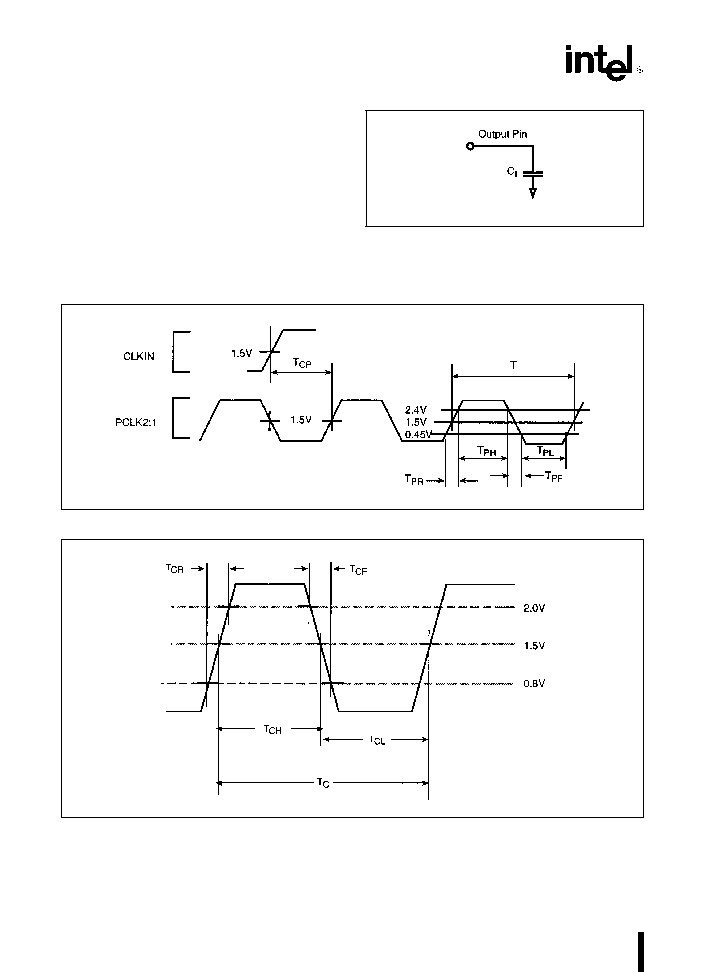
4 5 1 AC Test Conditions
The AC Specifications in Section 4 5 are tested with
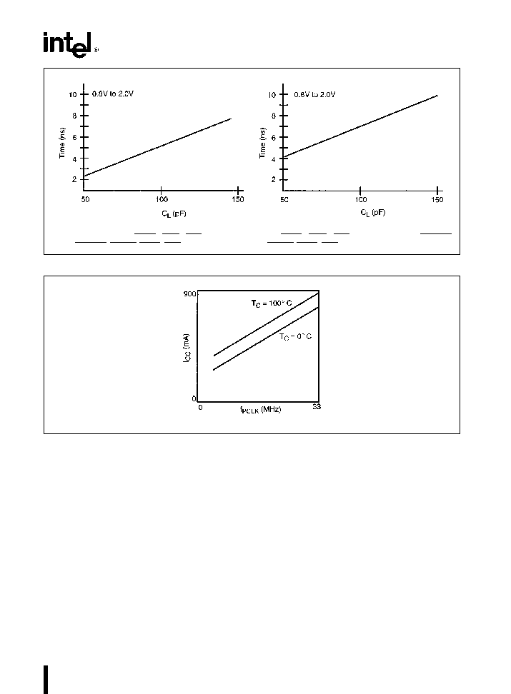
the 50 pF load shown in Figure 6 Figure 15 shows
how timings vary with load capacitance
Specifications are measured at the 1 5V crossing
point unless otherwise indicated Input waveforms
are assumed to have a rise and fall time of
s
2 ns
from 0 8V to 2 0V See Section 4 5 2 AC Timing
Waveforms
for AC spec definitions test points and
illustrations
271327 ≠ 6
C
L
e
50 pF for all signals
Figure 6 AC Test Load
4 5 2 AC Timing Waveforms
271327 ≠ 7
Figure 7 Input and Output Clock Waveforms
271327 ≠ 8
Figure 8 CLKIN Waveform
28
SPECIAL ENVIRONMENT 80960CA-25 -16
271327 ≠ 9
Figure 9 Output Delay and Float Waveform
271327 ≠ 10
Figure 10 Input Setup and Hold Waveform
T
OV
T
OH
OUTPUT DELAY
The maximum output delay is referred to as the Output Valid Delay (T
OV
) The
minimum output delay is referred to as the Output Hold (T
OH
)
T
OF
OUTPUT FLOAT DELAY
The output float condition occurs when the maximum output current
becomes less than I
LO
in magnitude
T
IS
T
IH
INPUT SETUP AND HOLD
The input setup and hold requirements specify the sampling window
during which synchronous inputs must be stable for correct processor operation
29
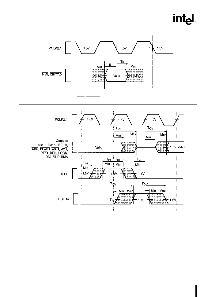
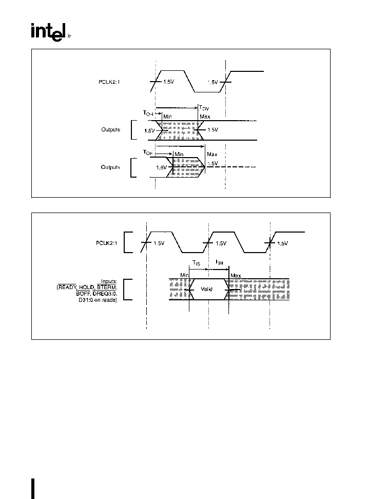
SPECIAL ENVIRONMENT 80960CA-25 -16
271327 ≠ 11
Figure 11 NMI XINT7 0 Input Setup and Hold Waveform
271327 ≠ 12
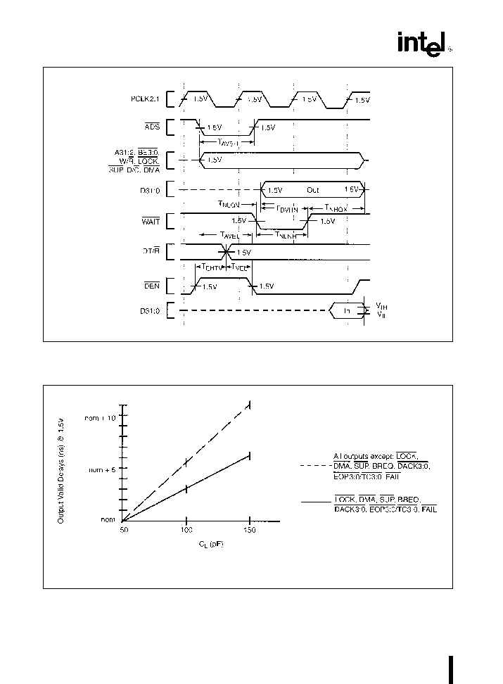
Figure 12 Hold Acknowledge Timings
T
OV
T
OH
OUTPUT DELAY
The maximum output delay is referred to as the Output Valid Delay (T
OV
) The
minimum output delay is referred to as the Output Hold (T
OH
)
T
OF
OUTPUT FLOAT DELAY
The output float condition occurs when the maximum output current
becomes less than I
LO
in magnitude
T
IS
T
IH
INPUT SETUP AND HOLD
The input setup and hold requirements specify the sampling window
during which synchronous inputs must be stable for correct processor operation
30
SPECIAL ENVIRONMENT 80960CA-25 -16
271327 ≠ 13
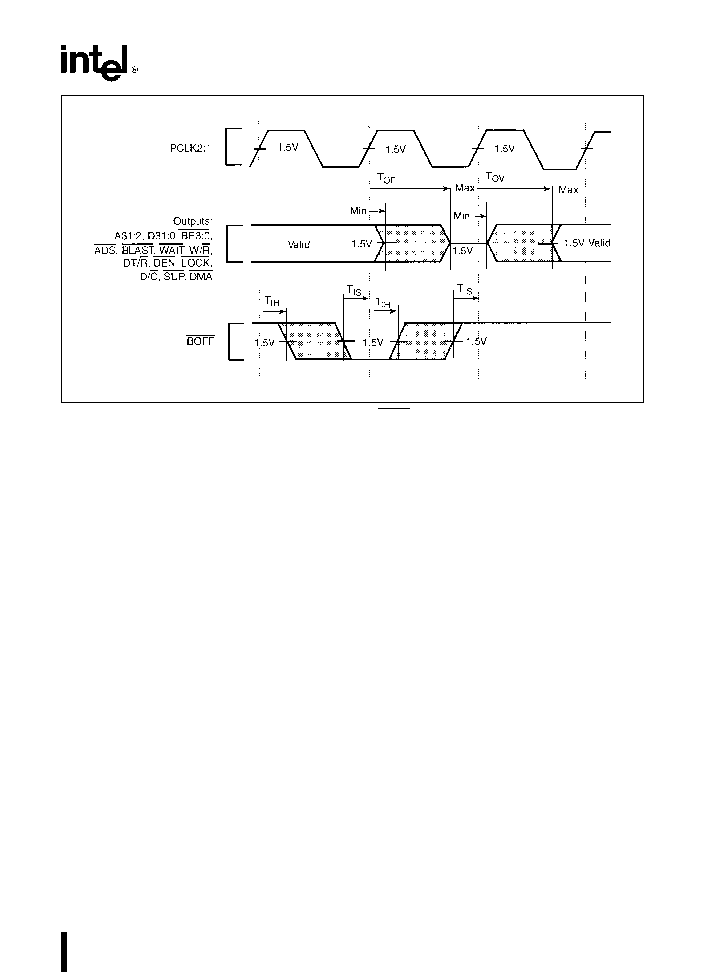
Figure 13 Bus Backoff BOFF Timings
31
SPECIAL ENVIRONMENT 80960CA-25 -16
271327 ≠ 14
Figure 14 Relative Timings Waveforms
4 5 3 Derating Curves
271327 ≠ 15
NOTE
PCLK Load
e
50 pF
Figure 15 Output Delay or Hold vs Load Capacitance
32
SPECIAL ENVIRONMENT 80960CA-25 -16
271327 ≠ 16
a) All outputs except
LOCK
DMA
SUP
HOLDA
BREQ DACK3 0 EOP3 0 TC3 0 FAIL
b) LOCK
DMA
SUP
HOLDA
BREQ
DACK3 0
EOP3 0 TC3 0 FAIL
Figure 16 Rise and Fall Time Derating at Highest Operating Temperature and Minimum V
CC
271327 ≠ 17
I
CC
≠ I
CC
under test conditions
Figure 17 I
CC
vs Frequency and Temperature
33
SPECIAL ENVIRONMENT 80960CA-25 -16
5 0 RESET BACKOFF AND HOLD
ACKNOWLEDGE
Table 15 lists the condition of each processor output
pin while RESET is asserted (low)
Table 15 Reset Conditions
Pins
State During Reset
(HOLDA Inactive)
1
A31 2
Floating
D31 0
Floating
BE3 0
Driven high (Inactive)
W R
Driven low (Read)
ADS
Driven high (Inactive)
WAIT
Driven high (Inactive)
BLAST
Driven low (Active)
DT R
Driven low (Receive)
DEN
Driven high (Inactive)
LOCK
Driven high (inactive)
BREQ
Driven low (Inactive)
D C
Floating
DMA
Floating
SUP
Floating
FAIL
Driven low (Active)
DACK3 0
Driven high (Inactive)
EOP3 0 TC3 0
Floating (Set to input mode)
NOTES
1 With regard to bus output pin state only the Hold Ac-
knowledge state takes precedence over the reset state
Although asserting the RESET pin will internally reset
the processor the processor's bus output pins will not
enter the reset state if it has granted Hold Acknowledge
to a previous HOLD request (HOLDA is active) Further-
more the processor will grant new HOLD requests and
enter the Hold Acknowledge state even while in reset
For example if HOLDA is inactive and the processor is
in the reset state then HOLD is asserted the process-
sor's bus pins enter the Hold Acknowledge state and
HOLDA is granted The processor will not be able to
perform memory accesses until the HOLD request is re-
moved even if the RESET pin is brought high This op-
eration is provided to simplify boot-up synchronization
among multiple processors sharing the same bus
Table 16 lists the condition of each processor output
pin while HOLDA is asserted (low)
Table 16 Hold Acknowledge and Backoff
Conditions
Pins
State During HOLDA
A31 2
Floating
D31 0
Floating
BE3 0
Floating
W R
Floating
ADS
Floating
WAIT
Floating
BLAST
Floating
DT R
Floating
DEN
Floating
LOCK
Floating
BREQ
Driven (High or low)
D C
Floating
DMA
Floating
SUP
Floating
FAIL
Driven high (Inactive)
DACK3 0
Driven high (Inactive)
EOP3 0 TC3 0
Driven (If output)
34
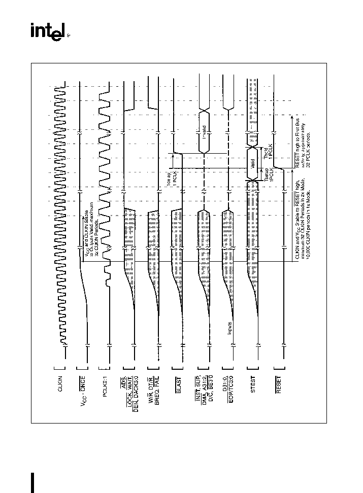
SPECIAL ENVIRONMENT 80960CA-25 -16
6 0 BUS WAVEFORMS
271327 ≠ 18
Figure 18 Cold Reset Waveform
35
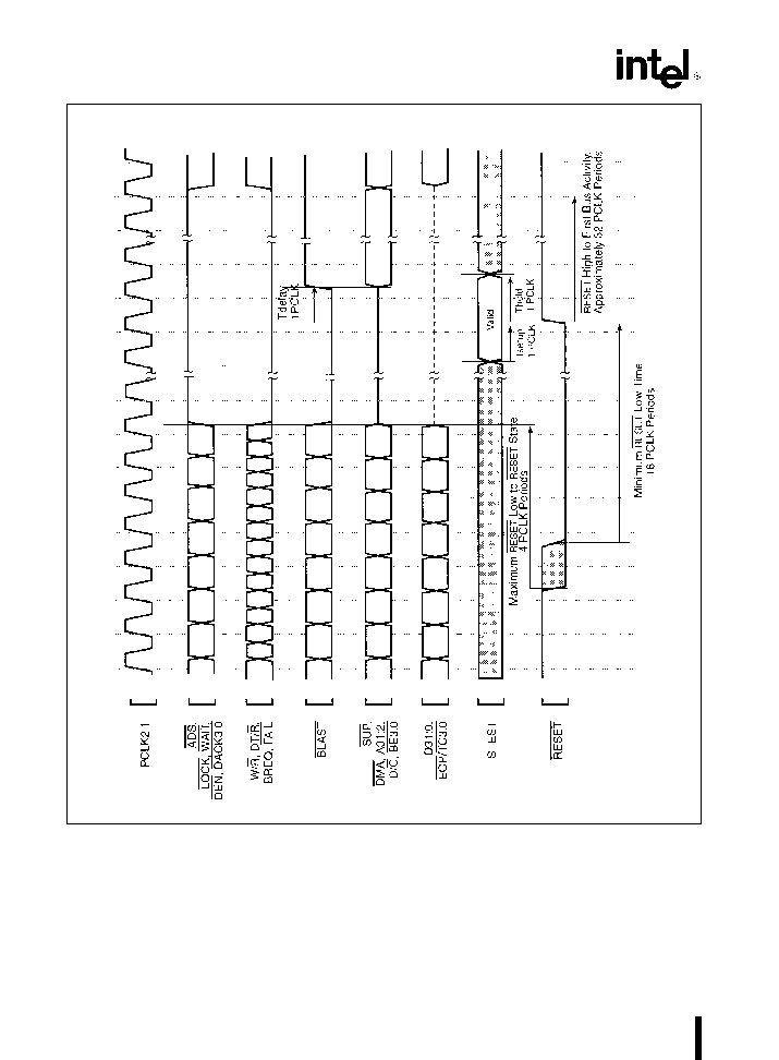
SPECIAL ENVIRONMENT 80960CA-25 -16
271327 ≠ 19
Figure 19 Warm Reset Waveform
36
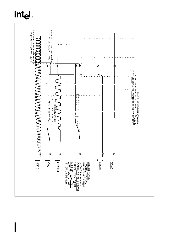
SPECIAL ENVIRONMENT 80960CA-25 -16
271327 ≠ 20
Figure 20 Entering the ONCE State
37
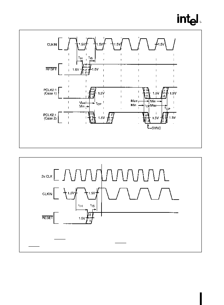
SPECIAL ENVIRONMENT 80960CA-25 -16
271327 ≠ 21
NOTE
Case 1 and Case 2 show two possible polarities of PCLK2 1
Figure 21 Clock Synchronization in the 2-x Clock Mode
271327 ≠ 22
NOTE
In 1x clock mode the RESET pin is actually sampled on the falling edge of 2xCLK 2xCLK is an internal signal generated
by the PLL and is not available on an external pin Therefore RESET is specified relative to the rising edge of CLKIN
The RESET pin is sampled when PCLK is high
Figure 22 Clock Synchronization in the 1-x Clock Mode
38
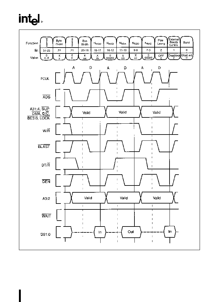
SPECIAL ENVIRONMENT 80960CA-25 -16
271327 ≠ 23
Figure 23 Non-Burst Non-Pipelined Requests Without Wait States
39
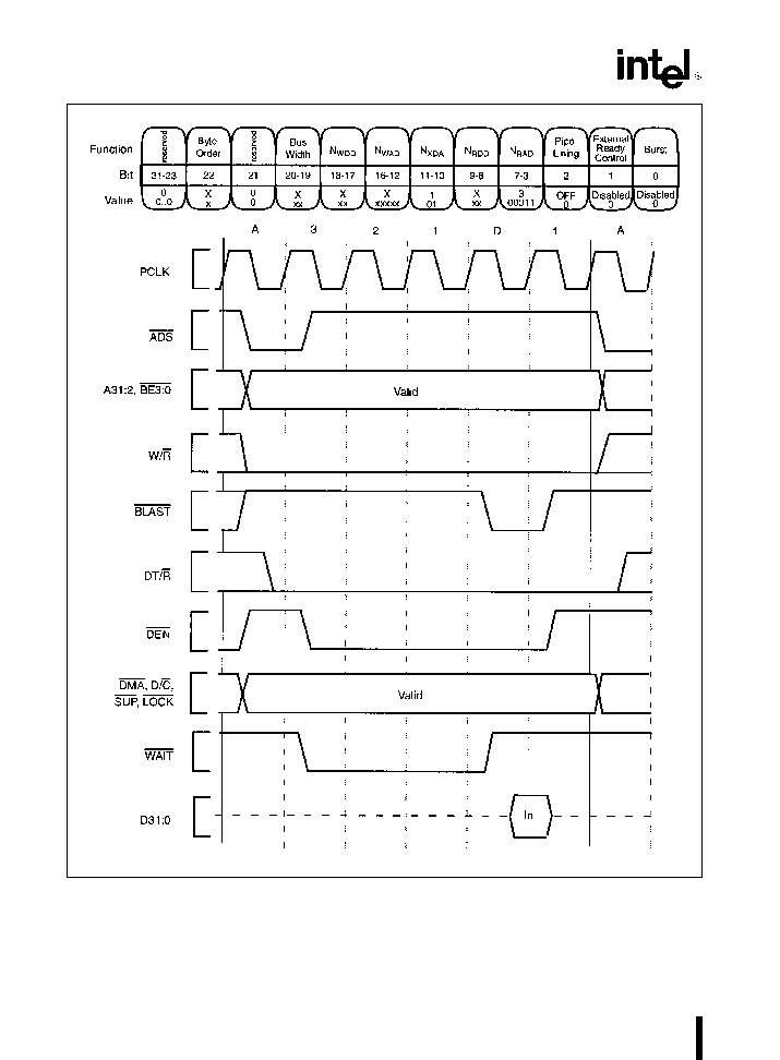
SPECIAL ENVIRONMENT 80960CA-25 -16
271327 ≠ 24
Figure 24 Non-Burst Non-Pipelined Read Request With Wait States
40
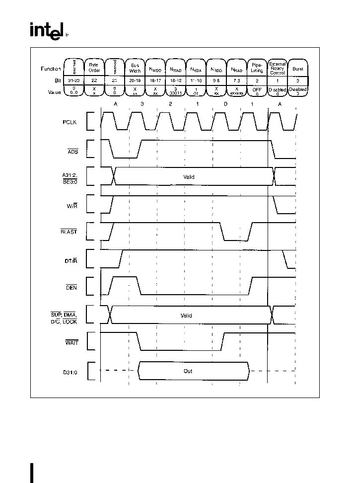
SPECIAL ENVIRONMENT 80960CA-25 -16
271327 ≠ 25
Figure 25 Non-Burst Non-Pipelined Write Request With Wait States
41
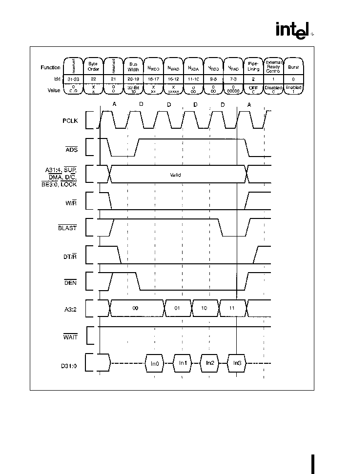
SPECIAL ENVIRONMENT 80960CA-25 -16
271327 ≠ 26
Figure 26 Burst Non-Pipelined Read Request Without Wait States 32-Bit Bus
42
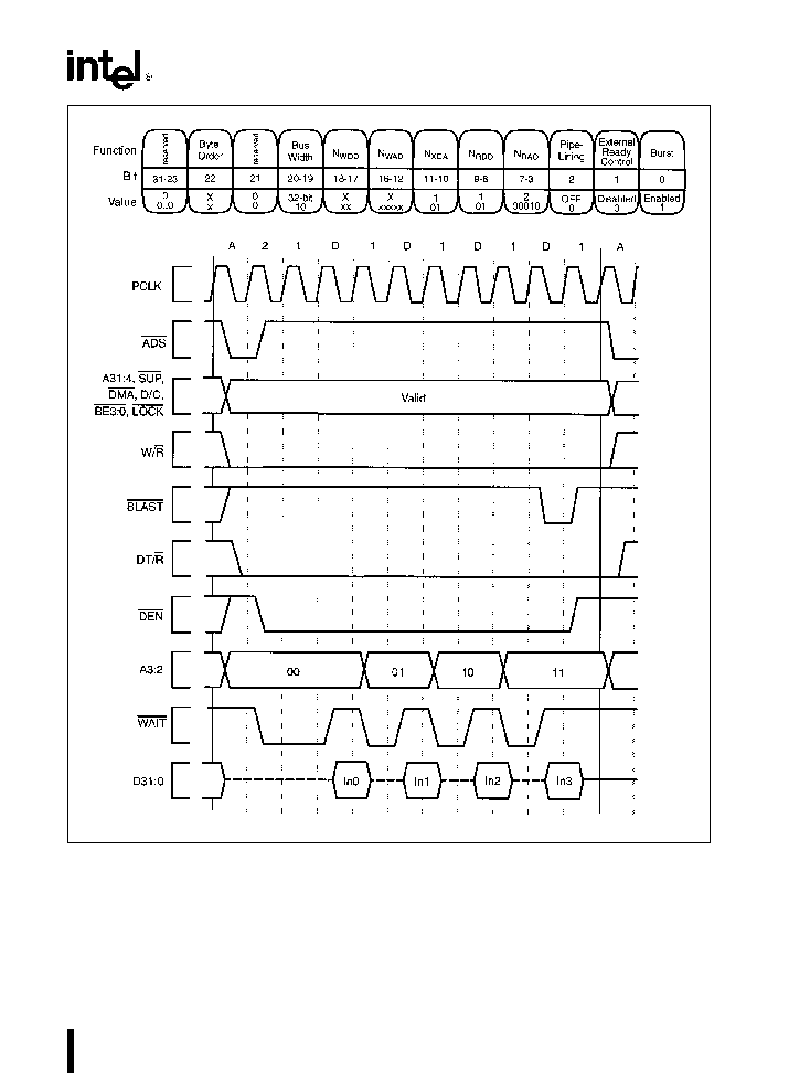
SPECIAL ENVIRONMENT 80960CA-25 -16
271327 ≠ 27
Figure 27 Burst Non-Pipelined Read Request With Wait States 32-Bit Bus
43
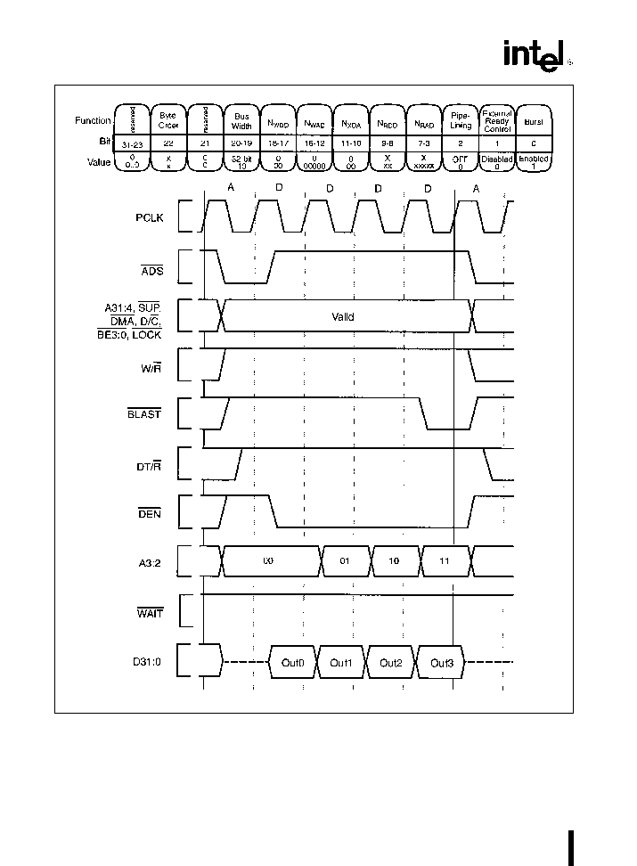
SPECIAL ENVIRONMENT 80960CA-25 -16
271327 ≠ 28
Figure 28 Burst Non-Pipelined Write Request Without Wait States 32-Bit Bus
44
SPECIAL ENVIRONMENT 80960CA-25 -16
271327 ≠ 29
Figure 29 Burst Non-Pipelined Write Request With Wait States 32-Bit Bus
45
SPECIAL ENVIRONMENT 80960CA-25 -16
271327 ≠ 30
Figure 30 Burst Non-Pipelined Read Request With Wait States 16-Bit Bus
46
SPECIAL ENVIRONMENT 80960CA-25 -16
271327 ≠ 31
Figure 31 Burst Non-Pipelined Read Request With Wait States 8-Bit Bus
47
SPECIAL ENVIRONMENT 80960CA-25 -16
271327 ≠ 32
Figure 32 Non-Burst Pipelined Read Request Without Wait States 32-Bit Bus
48
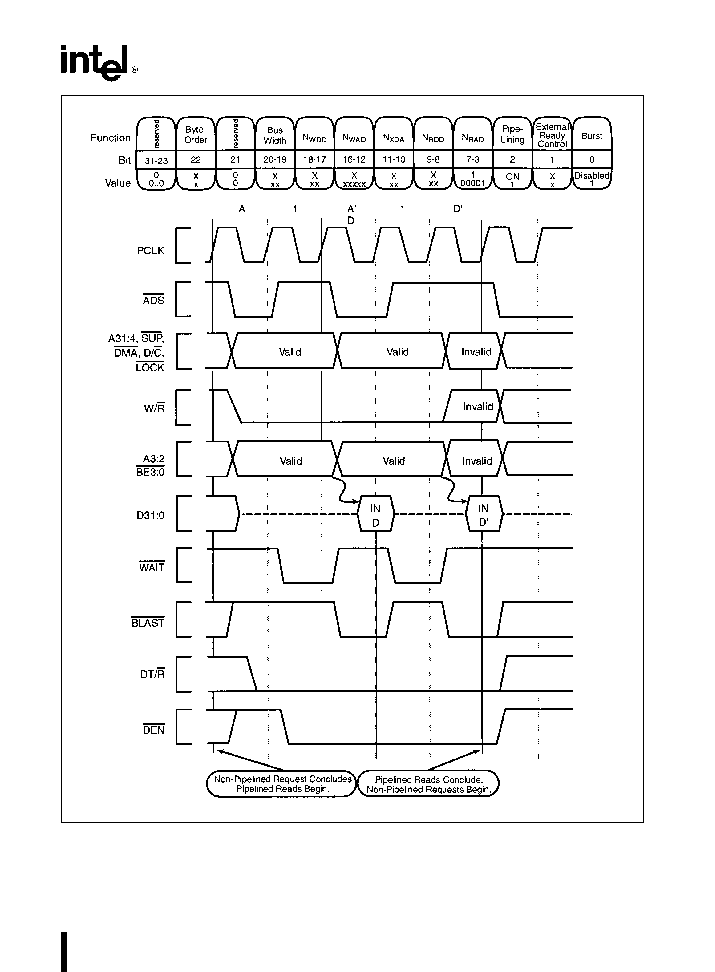
SPECIAL ENVIRONMENT 80960CA-25 -16
271327 ≠ 33
Figure 33 Non-Burst Pipelined Read Request With Wait States 32-Bit Bus
49
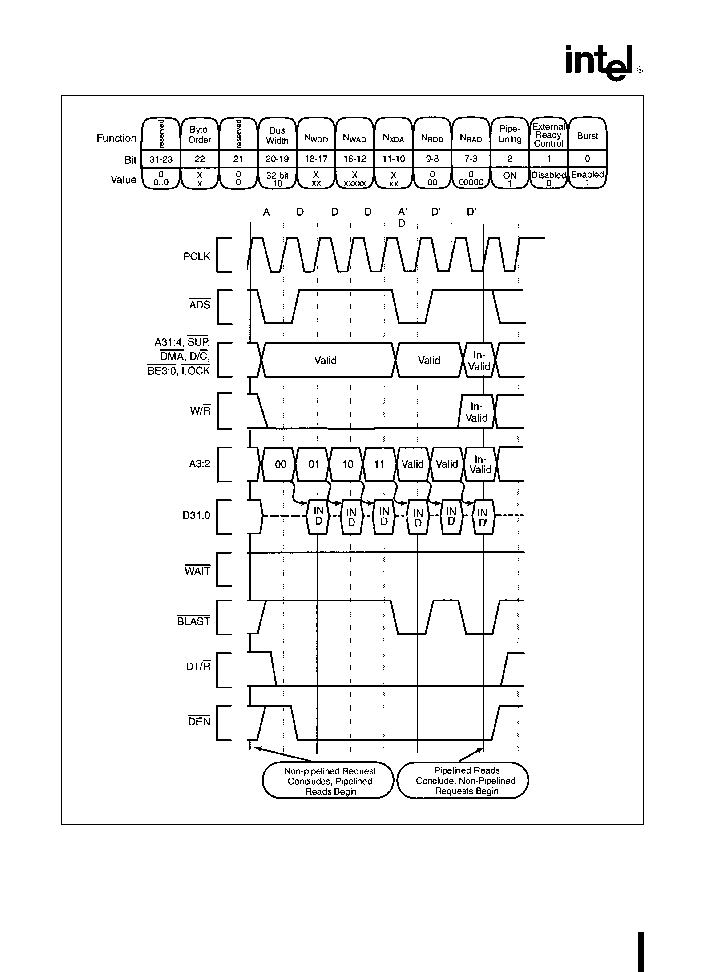
SPECIAL ENVIRONMENT 80960CA-25 -16
271327 ≠ 34
Figure 34 Burst Pipelined Read Request Without Wait States 32-Bit Bus
50
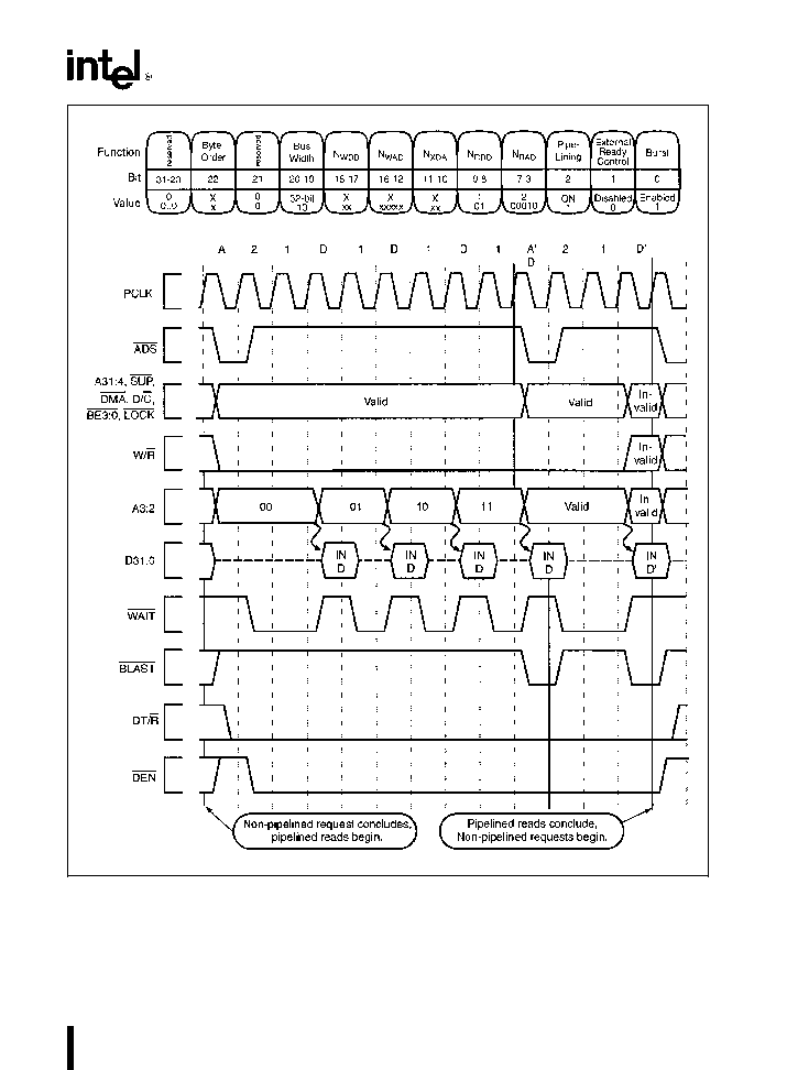
SPECIAL ENVIRONMENT 80960CA-25 -16
271327 ≠ 35
Figure 35 Burst Pipelined Read Request With Wait States 32-Bit Bus
51
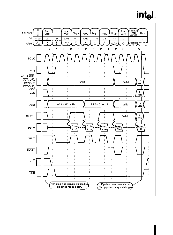
SPECIAL ENVIRONMENT 80960CA-25 -16
271327 ≠ 36
Figure 36 Burst Pipelined Read Request With Wait States 16-Bit Bus
52
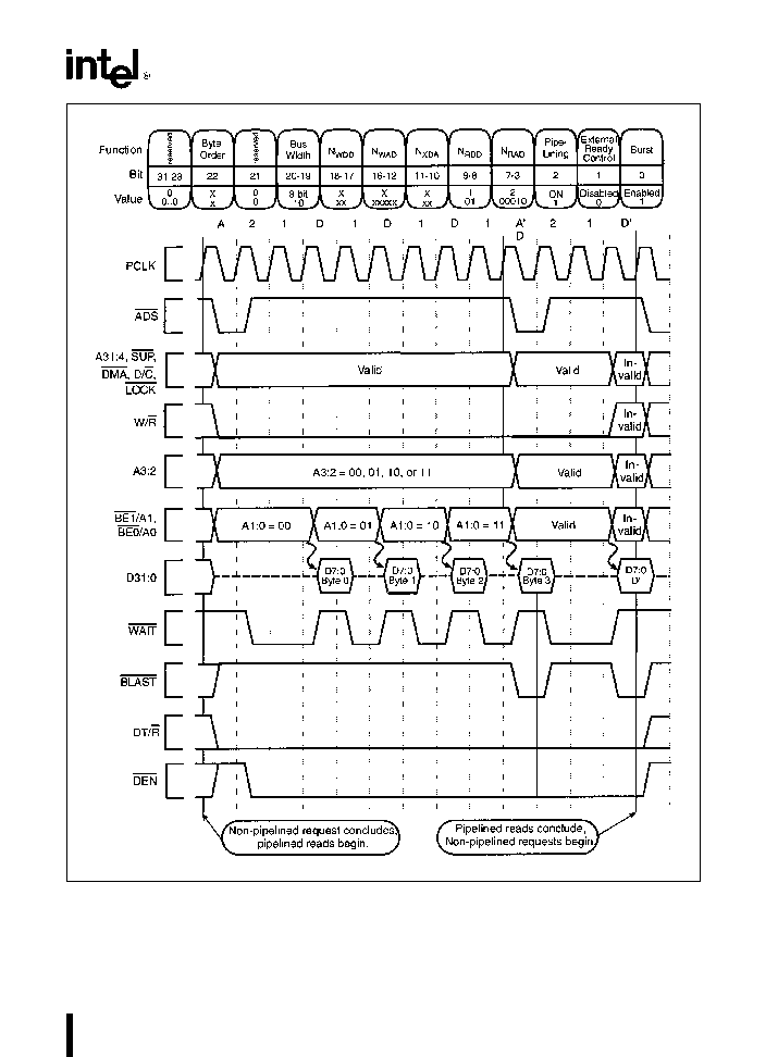
SPECIAL ENVIRONMENT 80960CA-25 -16
271327 ≠ 37
Figure 37 Burst Pipelined Read Request With Wait States 8-Bit Bus
53
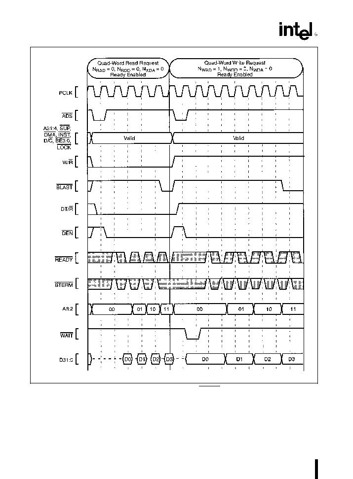
SPECIAL ENVIRONMENT 80960CA-25 -16
271327 ≠ 38
Figure 38 Using External READY
54
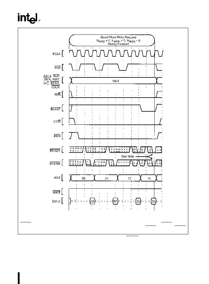
SPECIAL ENVIRONMENT 80960CA-25 -16
271327 ≠ 39
NOTE
READY adds memory access time to data transfers whether or not the bus access is a burst access BTERM interrupts
a bus access whether or not the bus access has more data transfers pending Either the READY signal or the BTERM
signal will terminate a bus access if the signal is asserted during the last (or only) data transfer of the bus access
Figure 39 Terminating a Burst with BTERM
55
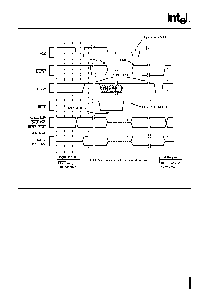
SPECIAL ENVIRONMENT 80960CA-25 -16
271327 ≠ 40
NOTE
READY BTERM must be enabled N
RAD
N
RDD
N
WAD
N
WDD
e
0
Figure 40 BOFF Functional Timing
56
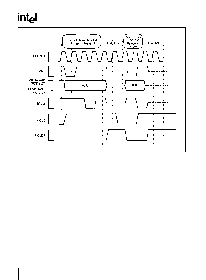
SPECIAL ENVIRONMENT 80960CA-25 -16
271327 ≠ 41
Figure 41 HOLD Functional Timing
57
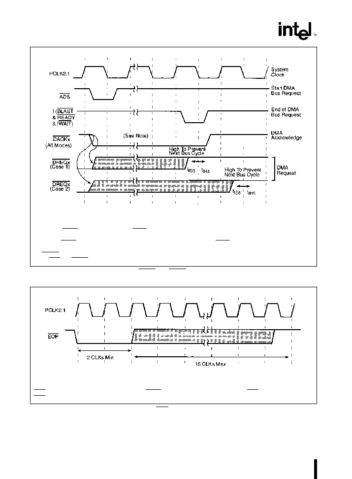
SPECIAL ENVIRONMENT 80960CA-25 -16
271327 ≠ 42
NOTES
1 Case 1 DREQ must deassert before DACK deasserts Applications are Fly-By and some packing and unpacking
modes in which loads are followed by loads or stores are followed by stores
2 Case 2 DREQ must be deasserted by the second clock (rising edge) after DACK is driven high Applications are non
Fly-By transfers and adjacent load-stores or store-loads
3 DACKx is asserted for the duration of a DMA bus request The request may consist of multiple bus accesses (defined
by ADS and BLAST Refer to
i960
CA Microprocessor User's Manual for ``access'' ``request'' definitions
Figure 42 DREQ and DACK Functional Timing
271327 ≠ 43
NOTE
EOP has the same AC Timing Requirements as DREQ to prevent unwanted DMA requests EOP is NOT edge triggered
EOP must be held for a minimum of 2 clock cycles then deasserted within 15 clock cycles
Figure 43 EOP Functional Timing
58
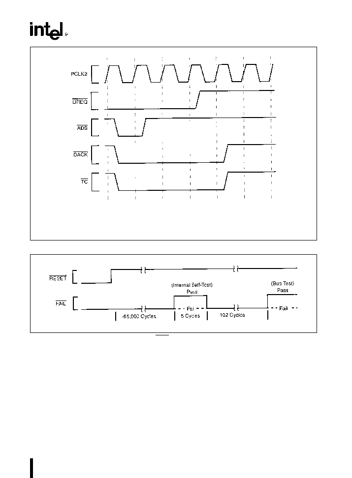
SPECIAL ENVIRONMENT 80960CA-25 -16
271327 ≠ 44
NOTES
Terminal Count becomes active during the last bus request of a buffer If the last LOAD STORE bus request is executed
as multiple bus accesses the TC will be active for the entire bus request Refer to the
i960
CA Microprocessor User's
Manual for further information
Figure 44 Terminal Count Functional Timing
271327 ≠ 45
Figure 45 FAIL Functional Timing
59
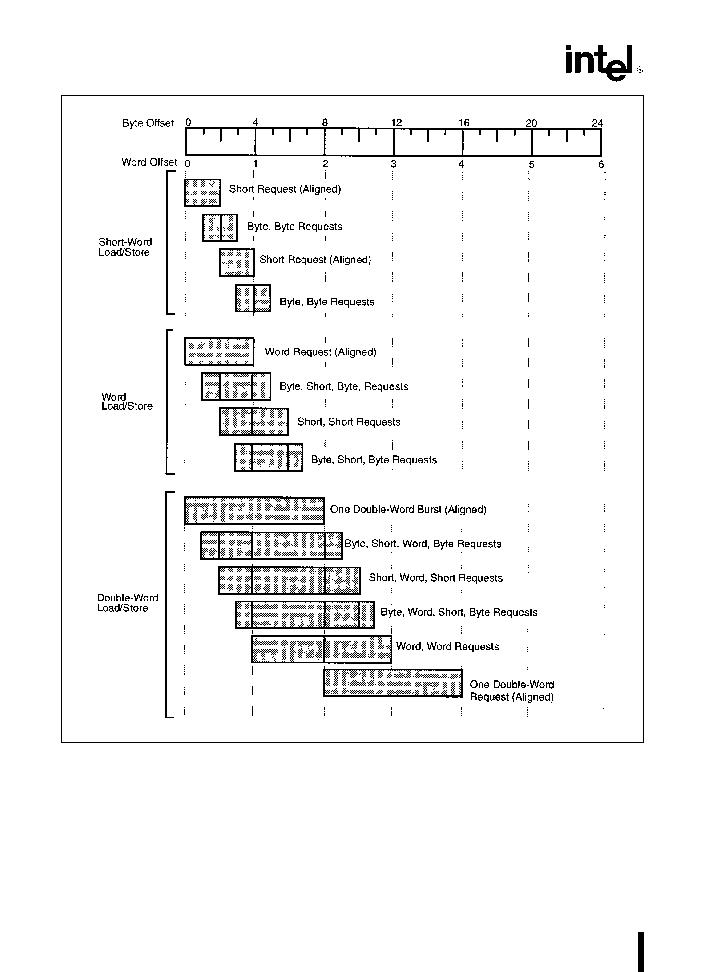
SPECIAL ENVIRONMENT 80960CA-25 -16
271327 ≠ 46
Figure 46 A Summary of Aligned and Unaligned Transfers for Little Endian Regions
60
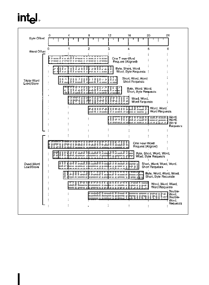
SPECIAL ENVIRONMENT 80960CA-25 -16
271327 ≠ 47
Figure 47 A Summary of Aligned and Unaligned Transfers for Little Endian Regions
(Continued)
61
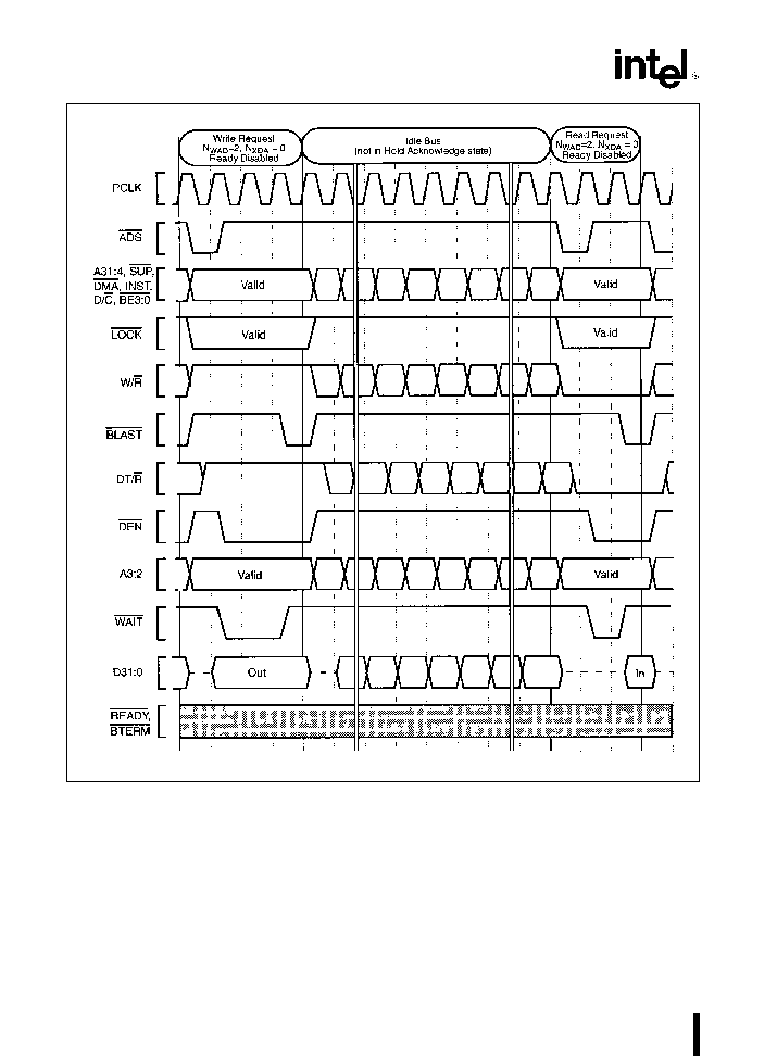
SPECIAL ENVIRONMENT 80960CA-25 -16
271327 ≠ 48
Figure 48 Idle Bus Operation
7 0 REVISION HISTORY
New
62