
Other brands and names are the property of their respective owners
Information in this document is provided in connection with Intel products Intel assumes no liability whatsoever including infringement of any patent or
copyright for sale and use of Intel products except as provided in Intel's Terms and Conditions of Sale for such products Intel retains the right to make
changes to these specifications at any time without notice Microcomputer Products may have minor variations to this specification known as errata
January 1995
COPYRIGHT
INTEL CORPORATION 1995
Order Number 271328-001
SPECIAL ENVIRONMENT 80960CF-30 -25 -16
32-BIT HIGH-PERFORMANCE SUPERSCALAR
PROCESSOR
Socket and Object Code Compatible with 80960CA
Two Instructions Clock Sustained Execution
Four 59 Mbytes s DMA Channels with Data Chaining
Demultiplexed 32-bit Burst Bus with Pipelining
Y
32-bit Parallel Architecture
Two Instructions clock Execution
Load Store Architecture
Sixteen 32-bit Global Registers
Sixteen 32-bit Local Registers
Manipulate 64-bit Bit Fields
11 Addressing Modes
Full Parallel Fault Model
Supervisor Protection Model
Y
Fast Procedure Call Return Model
Full Procedure Call in 4 clocks
Y
On-Chip Register Cache
Caches Registers on Call Ret
Minimum of 6 Frames provided
Up to 15 Programmable Frames
Y
On-Chip Instruction Cache
4 Kbyte Two-Way Set Associative
128-bit Path to Instruction Sequencer
Cache-Lock Modes
Cache-Off Mode
Y
On-Chip Data Cache
1 Kbyte Direct-Mapped
Write Through
128 bits per Clock Access on
Cache Hit
Y
Product Grades Available
SE3
b
40 C to
a
110 C
Y
High Bandwidth On-Chip Data RAM
1 Kbytes On-Chip RAM for Data
Sustain 128 bits per clock access
Y
Four On-Chip DMA Channels
59 Mbytes s Fly-by Transfers
32 Mbytes s Two-Cycle Transfers
Data Chaining
Data Packing Unpacking
Programmable Priority Method
Y
32-Bit Demultiplexed Burst Bus
128-bit Internal Data Paths to
and
from Registers
Burst Bus for DRAM Interfacing
Address Pipelining Option
Fully Programmable Wait States
Supports 8 16 or 32-bit Bus Widths
Supports Unaligned Accesses
Supervisor Protection Pin
Y
Selectable Big or Little Endian Byte
Ordering
Y
High-Speed Interrupt Controller
Up to 248 External Interrupts
32 Fully Programmable Priorities
Multi-mode 8-bit Interrupt Port
Four Internal DMA Interrupts
Separate Non-maskable Interrupt Pin
Context Switch in 750 ns Typical
SPECIAL ENVIRONMENT 80960CF-30 -25 -16
271328 ≠ 1
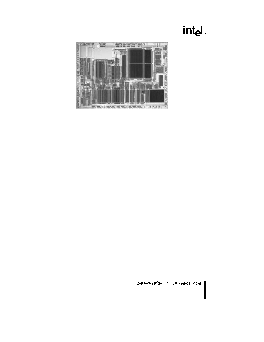
Figure 1 80960CF Die Photo
2

Special Environment 80960CF-30 -25 -16
32-Bit High Performance Superscalar Processor
CONTENTS
PAGE
1 0 PURPOSE
5
2 0 i960 CF PROCESSOR
OVERVIEW
5
2 1 The C-Series Core
6
2 2 Pipelined Burst Bus
6
2 3 Flexible DMA Controller
6
2 4 Priority Interrupt Controller
6
2 5 Instruction Set Summary
7
3 0 PACKAGE INFORMATION
8
3 1 Package Introduction
8
3 2 Pin Descriptions
8
3 3 80960CF Pinout
14
3 4 Mechanical Data
18
3 5 Package Thermal Specifications
20
3 6 Stepping Register Information
21
3 7 Suggested Sources for 80960CF
Accessories
21
4 0 ELECTRICAL SPECIFICATIONS
22
4 1 Absolute Maximum Ratings
22
4 2 Operating Conditions
22
4 3 Recommended Connections
22
4 4 DC Specifications
23
4 5 AC Specifications
24
5 0 RESET BACKOFF AND HOLD
ACKNOWLEDGE
35
6 0 BUS WAVEFORMS
36
CONTENTS
PAGE
FIGURES
Figure 1
80960CF Die Photo
2
Figure 2
80960CF Block Diagram
5
Figure 3
Example Pin Description
Entry
8
Figure 4a
80960CF PGA Pinout (View
from Top Side)
16
Figure 4b
80960CF PGA Pinout (View
from Bottom Side)
17
Figure 5
168-Lead Ceramic PGA
Package Dimensions
18
Figure 6
80960CF PGA Package
Thermal Characteristics
20
Figure 7
Measuring 80960CF PGA
Case Temperature
21
Figure 8
Register G0
21
Figure 9
AC Test Load
30
Figure 10a Input and Output Clocks
Waveform
30
Figure 10b CLKIN Waveform
30
Figure 11
Output Delay and Float
Waveform
31
Figure 12a Input Setup and Hold
Waveform
31
Figure 12b NMI XINT7 0 Input Setup
and Hold Waveform
31
Figure 13
Hold Acknowledge
Timings
32
Figure 14
Bus Back-Off (BOFF)
Timings
32
3

CONTENTS
PAGE
Figure 15
Relative Timings
Waveforms
33
Figure 16
Output Delay or Hold vs Load
Capacitance
33
Figure 17
Rise and Fall Time Derating at
Highest Operating
Temperature and Minimum
V
CC
34
Figure 18
I
CC
vs Frequency and
Temperature
34
Figure 19
Cold Reset Waveform
36
Figure 20
Warm Reset Waveform
37
Figure 21
Entering the ONCE State
38
Figure 22a Clock Synchronization in the
2x Clock Mode
39
Figure 22b Clock Synchronization in the
1x Clock Mode
39
Figure 23
Non-Burst Non-Pipelined
Requests without Wait
States
40
Figure 24
Non-Burst Non-Pipelined
Read Request with Wait
States
41
Figure 25
Non-Burst Non-Pipelined
Write Request with Wait
States
42
Figure 26
Burst Non-Pipelined Read
Request without Wait States
32-Bit Bus
43
Figure 27
Burst Non-Pipelined Read
Request with Wait States
32-Bit Bus
44
Figure 28
Burst Non-Pipelined Write
Request without Wait States
32-Bit Bus
45
Figure 29
Burst Non-Pipelined Write
Request with Wait States
32-Bit Bus
46
Figure 30
Burst Non-Pipelined Read
Request with Wait States
16-Bit Bus
47
CONTENTS
PAGE
Figure 31
Burst Non-Pipelined Read
Request with Wait States
8-Bit Bus
48
Figure 32
Non-Burst Pipelined Read
Request without Wait States
32-Bit Bus
49
Figure 33
Non-Burst Pipelined Read
Request with Wait States
32-Bit Bus
50
Figure 34
Burst Pipelined Read
Request without Wait States
32-Bit Bus
51
Figure 35
Burst Pipelined Read
Requests with Wait States
32-Bit Bus
52
Figure 36
Burst Pipelined Read
Requests with Wait States
16-Bit Bus
53
Figure 37
Burst Pipelined Read
Requests with Wait States
8-Bit Bus
54
Figure 38
Using External READY
55
Figure 39
Terminating a Burst with
BTERM
56
Figure 40
BOFF Functional Timing
57
Figure 41
HOLD Functional Timing
57
Figure 42
DREQ and DACK Functional
Timing
58
Figure 43
EOP Functional Timing
58
Figure 44
Terminal Count Functional
Timing
59
Figure 45
FAIL Functional Timing
59
Figure 46
A Summary of Aligned and
Unaligned Transfers for Little
Endian Regions
60
Figure 47
A Summary of Aligned and
Unaligned Transfers for Little
Endian Regions
(Continued)
61
Figure 48
Idle Bus Operation
62
4

SPECIAL ENVIRONMENT 80960CF-30 -25 -16
1 0
PURPOSE
This document previews electrical characterizations
of Intel's i960 CF embedded microprocessor (avail-
able in 33 25 and 16 MHz) For a detailed descrip-
tion of any i960 CF processor functional topic
oth-
er than parametric performance
refer to the latest
i960 CA Microprocessor Reference Manual (Order
No 270710) and the
i960 CF Reference Manual Ad-
dendum
(Order No 272188)
2 0
i960 CF PROCESSOR OVERVIEW
Intel's i960 CF microprocessor is the performance
follow-on product to the i960 CA processor The
i960 CF product is socket- and object code-compati-
ble with the CA this makes CA-to-CF design up-
grades straightforward The i960 CF processor's in-
struction cache is 4 Kbytes (CA device has 1 Kbyte)
CF data cache is 1 Kbyte (CA device has no data
cache) This extra cache on the CF product adds a
significant performance boost over the CA The
80960CF is object code compatible with the 32-bit
80960 Core Architecture while including Special
Function Register extensions to control on-chip pe-
ripherals and instruction set extensions to shift 64-
bit operands and configure on-chip hardware Multi-
ple 128-bit internal busses on-chip instruction cach-
ing and a sophisticated instruction scheduler allow
the processor to sustain execution of two instruc-
tions every clock and peak at execution of three
instructions per clock
A 32-bit demultiplexed and pipelined burst bus pro-
vides a 132 Mbyte s bandwidth to a system's high-
speed external memory sub-system In addition the
80960CF's on-chip caching of instructions proce-
dure context and critical program data substantially
decouples system performance from the wait states
associated with accesses to the system's slower
cost sensitive main memory sub-system
The 80960CF bus controller also integrates full wait
state and bus width control for highest system per-
formance with minimal system design complexity
Unaligned access and Big Endian byte order support
reduces the cost of porting existing applications to
the 80960CF
The processor also integrates four complete data-
chaining DMA channels and a high-speed interrupt
controller on-chip The DMA channels perform sin-
gle-cycle or two-cycle transfers data packing and
unpacking and data chaining Block transfers in ad-
dition to source or destination synchronized trans-
fers are provided
The interrupt controller provides full programmability
of 248 interrupt sources into 32 priority levels with a
typical interrupt task switch (``latency'') time of
750 ns
271328 ≠ 2
Figure 2 80960CF Block Diagram
5