Document Outline
- 80960JD EMBEDDED 32-BIT MICROPROCESSOR Cover Page
- Table of Contents
- List of Figures
- Figure 1. 80960JD Microprocessor
- Figure 2. 80960JD Block Diagram
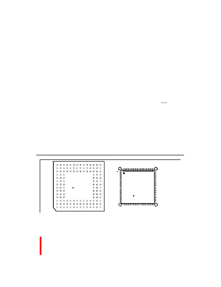
- Figure 3. 132-Lead Pin Grid Array Bottom View - Pins Facing Up
- Figure 4. 132-Lead Pin Grid Array Top View - Pins Facing Down
- Figure 5. 132-Lead PQFP - Top View
- Figure 6. 50 MHz Maximum Allowable Ambient Temperature
- Figure 7. 40 MHz Maximum Allowable Ambient Temperature
- Figure 8. AC Test Load
- Figure 9. Output Delay or Hold vs. Load Capacitance
- Figure 10. Rise and Fall Time Derating
- Figure 11. CLKIN Waveform
- Figure 12. Output Delay Waveform for T OV1
- Figure 13. Output Float Waveform for T OF
- Figure 14. Input Setup and Hold Waveform for T IS1 and T IH1
- Figure 15. Input Setup and Hold Waveform for T IS2 and T IH2
- Figure 16. Input Setup and Hold Waveform for T IS3 and T IH3
- Figure 17. Input Setup and Hold Waveform for T IS4 and T IH4
- Figure 18. Relative Timings Waveform for T LXL and T LXA
- Figure 19. DT/R and DEN Timings Waveform
- Figure 20. TCK Waveform
- Figure 21. Input Setup and Hold Waveforms for T BSIS1 and T BSIH1
- Figure 22. Output Delay and Output Float Waveform for T BSOV1 AND T BSOF1
- Figure 23. Output Delay and Output Float Waveform for T BSOV2 and T BSOF2
- Figure 24. Input Setup and Hold Waveform for T BSIS2 and T BSIH2
- Figure 25. Non-Burst Read and Write Transactions Without Wait States, 32-Bit Bus
- Figure 26. Burst Read and Write Transactions Without Wait States, 32-Bit Bus
- Figure 27. Burst Write Transactions With 2,1,1,1 Wait States, 32-Bit Bus
- Figure 28. Burst Read and Write Transactions Without Wait States, 8-Bit Bus
- Figure 29. Burst Read and Write Transactions With 1, 0 Wait States and Extra Tr State on Read, 16-Bit Bus
- Figure 30. Bus Transactions Generated by Double Word Read Bus Request, Misaligned One Byte From Quad Word Boundary, 32-Bit Bus,
- Figure 31. HOLD/HOLDA Waveform For Bus Arbitration
- Figure 32. Cold Reset Waveform
- Figure 33. Warm Reset Waveform
- Figure 34. Entering the ONCE State
- Figure 35. Summary of Aligned and Unaligned Accesses (32-Bit Bus)
- Figure 36. Summary of Aligned and Unaligned Accesses (32-Bit Bus) (Continued)
- List of Tables
- 1.0 PURPOSE
- 2.0 80960JD OVERVIEW
- 3.0 PACKAGE INFORMATION
- 4.0 ELECTRICAL SPECIFICATIONS
- 5.0 BUS FUNCTIONAL WAVEFORMS
- 6.0 DEVICE IDENTIFICATION
- 7.0 REVISION HISTORY
Information in this document is provided solely to enable use of Intel products. Intel assumes no liability whatsoever, including infringement of any
patent or copyright, for sale and use of Intel products except as provided in Intel's Terms and Conditions of Sale for such products. Information
contained herein supersedes previously published specifications on these devices from Intel.
© INTEL CORPORATION, 1995
September 1995
Order Number: 272596-002
PRELIMINARY
80960JD
EMBEDDED 32-BIT MICROPROCESSOR
Figure 1. 80960JD Microprocessor
s
Pin/Code Compatible with all 80960Jx
Processors
s
High-Performance Embedded Architecture
-- One Instruction/Clock Execution
-- Core Clock Rate is 2x the Bus Clock
-- Load/Store Programming Model
-- Sixteen 32-Bit Global Registers
-- Sixteen 32-Bit Local Registers (8 sets)
-- Nine Addressing Modes
-- User/Supervisor Protection Model
s
Two-Way Set Associative Instruction Cache
-- 80960JD - 4 Kbyte
-- Programmable Cache Locking
Mechanism
s
Direct Mapped Data Cache
-- 80960JD - 2 Kbyte
-- Write Through Operation
s
On-Chip Stack Frame Cache
-- Seven Register Sets Can Be Saved
-- Automatic Allocation on Call/Return
-- 0-7 Frames Reserved for High-Priority
Interrupts
s
On-Chip Data RAM
-- 1 Kbyte Critical Variable Storage
-- Single-Cycle Access
s
High Bandwidth Burst Bus
-- 32-Bit Multiplexed Address/Data
-- Programmable Memory Configuration
-- Selectable 8-, 16-, 32-Bit Bus Widths
-- Supports Unaligned Accesses
-- Big or Little Endian Byte Ordering
s
New Instructions
-- Conditional Add, Subtract and Select
-- Processor Management
s
High-Speed Interrupt Controller
-- 31 Programmable Priorities
-- Eight Maskable Pins plus NMI
-- Up to 240 Vectors in Expanded Mode
s
Two On-Chip Timers
-- Independent 32-Bit Counting
-- Clock Prescaling by 1, 2, 4 or 8
-- lnternal Interrupt Sources
s
Halt Mode for Low Power
s
IEEE 1149.1 (JTAG) Boundary Scan
Compatibility
s
Packages
-- 132-Lead Pin Grid Array (PGA)
-- 132-Lead Plastic Quad Flat Pack (PQFP)
PIN 1
132
99
66
33
i960
Æ
i
M
i
© 19xx
M
© 19xx
A80960JD
NG80960JD
XXXXXXXXA2
XXXXXXXXA2

PRELIMINARY
ii
80960JD
80960JD
EMBEDDED 32-BIT MICROPROCESSOR
1.0 PURPOSE ..................................................................................................................................................1
2.0 80960JD OVERVIEW ................................................................................................................................. 1
2.1 80960 Processor Core ........................................................................................................................2
2.2 Burst Bus ............................................................................................................................................2
2.3 Timer Unit ...........................................................................................................................................3
2.4 Priority Interrupt Controller .................................................................................................................3
2.5 Instruction Set Summary ....................................................................................................................3
2.6 Faults and Debugging .........................................................................................................................3
2.7 Low Power Operation .........................................................................................................................4
2.8 Test Features ......................................................................................................................................4
2.9 Memory-Mapped Control Registers ....................................................................................................4
2.10 Data Types and Memory Addressing Modes ....................................................................................4
3.0 PACKAGE INFORMATION ........................................................................................................................6
3.1 Pin Descriptions .................................................................................................................................. 6
3.1.1 Functional Pin Definitions ........................................................................................................6
3.1.2 80960Jx 132-Lead PGA Pinout .............................................................................................13
3.1.3 80960Jx PQFP Pinout ...........................................................................................................17
3.2 Package Thermal Specifications ......................................................................................................20
3.3 Thermal Management Accessories ..................................................................................................22
4.0 ELECTRICAL SPECIFICATIONS ............................................................................................................23
4.1 Absolute Maximum Ratings ..............................................................................................................23
4.2 Operating Conditions ........................................................................................................................23
4.3 Connection Recommendations .........................................................................................................24
4.4 DC Specifications .............................................................................................................................24
4.5 AC Specifications ..............................................................................................................................26
4.5.1 AC Test Conditions and Derating Curves ...............................................................................33
4.5.2 AC Timing Waveforms ............................................................................................................34
5.0 BUS FUNCTIONAL WAVEFORMS .........................................................................................................42
6.0 DEVICE IDENTIFICATION .......................................................................................................................56
7.0 REVISION HISTORY ...............................................................................................................................56

iii
PRELIMINARY
80960JD
FIGURES
Figure 1.
80960JD Microprocessor ...........................................................................................................0
Figure 2.
80960JD Block Diagram ............................................................................................................2
Figure 3.
132-Lead Pin Grid Array Bottom View - Pins Facing Up .......................................................... 13
Figure 4.
132-Lead Pin Grid Array Top View - Pins Facing Down ........................................................... 14
Figure 5.
132-Lead PQFP - Top View ..................................................................................................... 17
Figure 6.
50 MHz Maximum Allowable Ambient Temperature ................................................................ 21
Figure 7.
40 MHz Maximum Allowable Ambient Temperature ................................................................ 22
Figure 8.
AC Test Load ............................................................................................................................ 33
Figure 9.
Output Delay or Hold vs. Load Capacitance ............................................................................ 33
Figure 10.
Rise and Fall Time Derating ..................................................................................................... 34
Figure 11.
CLKIN Waveform ..................................................................................................................... 34
Figure 12.
Output Delay Waveform for T
OV1
............................................................................................. 35
Figure 13.
Output Float Waveform for T
OF
................................................................................................ 35
Figure 14.
Input Setup and Hold Waveform for T
IS1
and T
IH1
................................................................... 36
Figure 15.
Input Setup and Hold Waveform for T
IS2
and T
IH2
................................................................... 36
Figure 16.
Input Setup and Hold Waveform for T
IS3
and T
IH3
................................................................... 37
Figure 17.
Input Setup and Hold Waveform for T
IS4
and T
IH4
................................................................... 37
Figure 18.
Relative Timings Waveform for T
LXL
and T
LXA
......................................................................... 38
Figure 19.
DT/R and DEN Timings Waveform .......................................................................................... 38
Figure 20.
TCK Waveform ......................................................................................................................... 39
Figure 21.
Input Setup and Hold Waveforms for T
BSIS1
and T
BSIH1
......................................................... 39
Figure 22.
Output Delay and Output Float Waveform for T
BSOV1
and T
BSOF1
.......................................... 40
Figure 23.
Output Delay and Output Float Waveform for T
BSOV2
and T
BSOF2
.......................................... 40
Figure 24.
Input Setup and Hold Waveform for T
BSIS2
and T
BSIH2
........................................................... 41
Figure 25.
Non-Burst Read and Write Transactions Without Wait States, 32-Bit Bus ............................... 42
Figure 26.
Burst Read and Write Transactions Without Wait States, 32-Bit Bus ...................................... 43
Figure 27.
Burst Write Transactions With 2,1,1,1 Wait States, 32-Bit Bus ................................................ 44
Figure 28.
Burst Read and Write Transactions Without Wait States, 8-Bit Bus ........................................ 45
Figure 29.
Burst Read and Write Transactions With 1, 0 Wait States
and Extra Tr State on Read, 16-Bit Bus ................................................................................... 46
Figure 30.
Bus Transactions Generated by Double Word Read Bus Request,
Misaligned One Byte From Quad Word Boundary, 32-Bit Bus, Little Endian ........................... 47
Figure 31.
HOLD/HOLDA Waveform For Bus Arbitration .......................................................................... 48
Figure 32.
Cold Reset Waveform .............................................................................................................. 49
Figure 33.
Warm Reset Waveform ............................................................................................................ 50
Figure 34.
Entering the ONCE State ......................................................................................................... 51
Figure 35.
Summary of Aligned and Unaligned Accesses (32-Bit Bus) .................................................... 54
Figure 36.
Summary of Aligned and Unaligned Accesses (32-Bit Bus) (Continued) ................................ 55

PRELIMINARY
iv
80960JD
TABLES
Table 1.
80960Jx Instruction Set ................................................................................................................ 5
Table 2.
Pin Description Nomenclature ...................................................................................................... 6
Table 3.
Pin Description -- External Bus Signals ...................................................................................... 7
Table 4.
Pin Description -- Processor Control Signals, Test Signals and Power ..................................... 10
Table 5.
Pin Description -- Interrupt Unit Signals .................................................................................... 12
Table 6.
132-Lead PGA Pinout -- In Signal Order ................................................................................... 15
Table 7.
132-Lead PGA Pinout -- In Pin Order ....................................................................................... 16
Table 8.
132-Lead PQFP Pinout -- In Signal Order ................................................................................ 18
Table 9.
132-Lead PQFP Pinout -- In Pin Order ..................................................................................... 19
Table 10.
132-Lead PGA Package Thermal Characteristics ...................................................................... 20
Table 11.
132-Lead PQFP Package Thermal Characteristics ................................................................... 21
Table 12.
80960JD Operating Conditions .................................................................................................. 23
Table 13.
80960JD DC Characteristics ...................................................................................................... 24
Table 14.
80960JD I
CC
Characteristics ...................................................................................................... 25
Table 15.
80960JD AC Characteristics (50 MHz) ...................................................................................... 26
Table 16.
Note Definitions for Table 15, 80960JD AC Characteristics (50 MHz) ...................................... 28
Table 17.
80960JD AC Characteristics (40 MHz) ...................................................................................... 28
Table 18.
80960JD AC Characteristics (33 MHz) ...................................................................................... 31
Table 19.
Natural Boundaries for Load and Store Accesses ..................................................................... 52
Table 20.
Summary of Byte Load and Store Accesses .............................................................................. 52
Table 21.
Summary of Short Word Load and Store Accesses ................................................................... 52
Table 22.
Summary of n-Word Load and Store Accesses (n = 1, 2, 3, 4) .................................................. 53
Table 23.
80960JD Die and Stepping Reference ....................................................................................... 56
Table 24.
Data Sheet Version -001 to -002 Revision History ..................................................................... 56

80960JD
PRELIMINARY
1
1.0
PURPOSE
This document contains advance information for the
80960JD microprocessor, including electrical
characteristics and package pinout information.
Detailed functional descriptions -- other than
parametric performance -- are published in the
i960
Æ
Jx Microprocessor User's Guide (272483).
Throughout this data sheet, references to "80960Jx"
indicate features which apply to all of the following:
∑ 80960JA -- 5V, 2 Kbyte instruction cache, 1 Kbyte
data cache
∑ 80960JF -- 5V, 4 Kbyte instruction cache, 2 Kbyte
data cache
∑ 80960JD -- 5V, 4 Kbyte instruction cache, 2 Kbyte
data cache and clock doubling
∑ 80L960JA -- 3.3 V version of the 80960JA
∑ 80L960JF -- 3.3 V version of the 80960JF
2.0
80960JD OVERVIEW
The 80960JD offers high performance to cost-
sensitive 32-bit embedded applications. The
80960JD is object code compatible with the 80960
Core Architecture and is capable of sustained
execution at the rate of one instruction per clock.
This processor's features include generous
instruction cache, data cache and data RAM. It also
boasts a fast interrupt mechanism, dual program-
mable timer units and new instructions.
The 80960JD's clock doubler operates the processor
core at twice the bus clock rate to improve execution
performance without increasing the complexity of
board designs.
Memory subsystems for cost-sensitive embedded
applications often impose substantial wait state
penalties. The 80960JD integrates considerable
storage resources on-chip to decouple CPU
execution from the external bus.
The 80960JD rapidly allocates and deallocates local
register sets during context switches. The processor
needs to flush a register set to the stack only when it
saves more than seven sets to its local register
cache.
A 32-bit multiplexed burst bus provides a high-speed
interface to system memory and I/O. A full
complement of control signals simplifies the
connection of the 80960JD to external components.
The user programs physical and logical memory
attributes through memory-mapped control registers
(MMRs) -- an extension not found on the i960 Kx,
Sx or Cx processors. Physical and logical configu-
ration registers enable the processor to operate with
all combinations of bus width and data object
alignment. The processor supports a homogeneous
byte ordering model.
This processor integrates two important peripherals:
a timer unit and an interrupt controller. These and
other hardware resources are programmed through
memory-mapped control registers, an extension to
the familiar 80960 architecture.
The timer unit (TU) offers two independent 32-bit
timers for use as real-time system clocks and
general-purpose system timing. These operate in
either single-shot or auto-reload mode and can
generate interrupts.
The interrupt controller unit (ICU) provides a flexible
means for requesting interrupts. The ICU provides
full programmability of up to 240 interrupt sources
into 31 priority levels. The ICU takes advantage of a
cached priority table and optional routine caching to
minimize interrupt latency. Clock doubling reduces
interrupt latency by 40% compared to the
80960JA/JF. Local registers may be dedicated to
high-priority interrupts to further reduce latency.
Acting independently from the core, the ICU
compares the priorities of posted interrupts with the
current process priority, off-loading this task from the
core. The ICU also supports the integrated timer
interrupts.
The 80960JD features a Halt mode designed to
support applications where low power consumption
is critical. The halt instruction shuts down instruction
execution, resulting in a power savings of up to 90
percent.
The 80960JD's testability features, including ONCE
(On-Circuit Emulation) mode and Boundary Scan
(JTAG), provide a powerful environment for design
debug and fault diagnosis.
The Solutions960Æ program features a wide variety
of development tools which support the i960
processor family. Many of these tools are developed
by partner companies; some are developed by Intel,
such as profile-driven optimizing compilers. For more
information on these products, contact your local
Intel representative.