 | –≠–ª–µ–∫—Ç—Ä–æ–Ω–Ω—ã–π –∫–æ–º–ø–æ–Ω–µ–Ω—Ç: 82093AA | –°–∫–∞—á–∞—Ç—å:  PDF PDF  ZIP ZIP |
PRELIMINARY
Information in this document is provided in connection with Intel products. No license, express or implied, by estoppel or otherwise, to any intellectual property
rights is granted by this document or by the sale of Intel products. Except as provided in Intel's Terms and Conditions of Sale for such products, Intel assumes no
liability whatsoever, and Intel disclaims any express or implied warranty, relating to sale and/or use of Intel products including liability or warranties relating to
fitness for a particular purpose, merchantability, or infringement of any patent, copyright or other intellectual property right. Intel products are not intended for use in
medical, life saving, or life sustaining applications. Intel retains the right to make changes to specifications and product descriptions at any time, without notice. The
82093AA IOAPIC may contain design defects or errors known as errata. Current characterized errata are available on request. Third-party brands and names are
the property of their respective owners.
© INTEL CORPORATION 1996
May 1996
Order Number: 290566-001
Provides Multiprocessor Interrupt
Management
Dynamic Interrupt Distribution-
Routing Interrupt to the Lowest
Priority Processor
Software Programmable Control of
Interrupt Inputs
Off Loads Interrupt Related Traffic
From the Memory Bus
24 Programmable Interrupts
13 ISA Interrupts Supported
4 PCI Interrupts
1 Interrupt/SMI# Rerouting
2 Motherboard Interrupts
1 Interrupt Used for INTR Input
3 General Purpose Interrupts
Independently Programmable for
Edge/Level Sensitivity Interrupts
Each Interrupt Can Be Programmed
to Respond to Active High or Low
Inputs
X-Bus Interface
CS For Flexible Decode of the
IOAPIC Device.
Index Register Interface for
Optimum Memory Usage
Registers are 32-Bit Wide to Match
the PCI to Host Bridge Architecture
Package 64-Pin PQFP
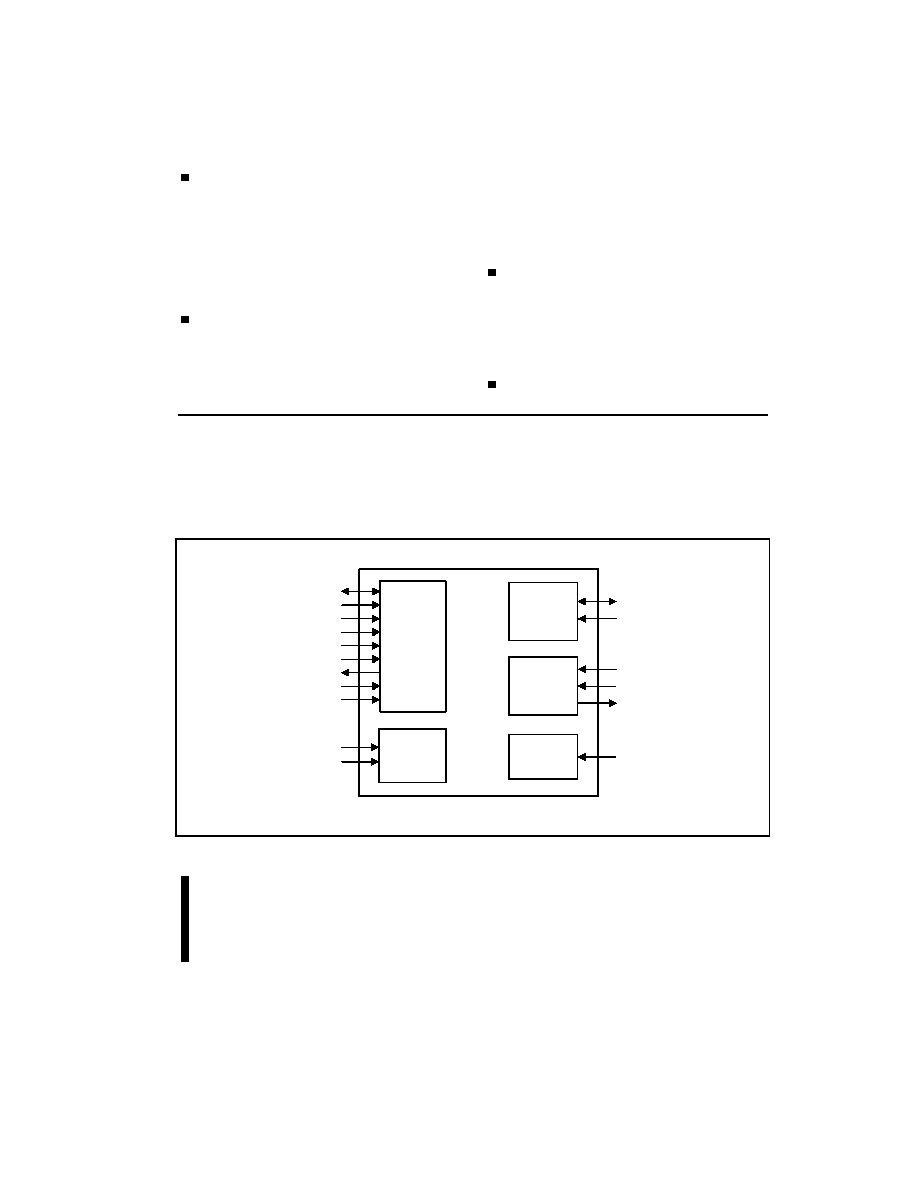
The 82093AA I/O Advanced Programmable Interrupt Controller (IOAPIC) provides multi-processor interrupt
management and incorporates both static and dynamic symmetric interrupt distribution across all processors. In
systems with multiple I/O subsystems, each subsystem can have its own set of interrupts. Each interrupt pin is
individually programmable as either edge or level triggered. The interrupt vector and interrupt steering
information can be specified per interrupt. An indirect register accessing scheme optimizes the memory space
needed to access the IOAPIC's internal registers. To increase system flexibility when assigning memory space
usage, the The IOAPIC's 2-register memory space is re-locatable.
System
Bus
Interface
APIC
Bus
Interface
Clock
And
Reset
D[7:0]
D/I#
A[1:0]
RD#
WR#
CS#
APCIREQ#
APICACK1#
APICACK2#
RESET
CLK
APCID[1:0]
APCICLK
APCID[1:0]
APCICLK
APCICLK
Interrupt
Controller
Test
TESTIN#
IOA_BLK
Figure 1. IOAPIC Simplified Block Diagram
82093AA I/O ADVANCED
PROGRAMMABLE INTERRUPT
CONTROLLER (IOAPIC)

82093AA (IOAPIC)
2
PRELIMINARY
CONTENTS
PAGE
1.0. OVERVIEW ......................................................................................................................................................3
2.0. SIGNAL DESCRIPTION ..................................................................................................................................5
2.1. System Bus Signals......................................................................................................................................5
2.2. Clock and Reset Signals...............................................................................................................................6
2.3. APIC Bus Interface .......................................................................................................................................6
2.4. Interrupt Signals ............................................................................................................................................6
2.5. Test and Power Signals ................................................................................................................................7
3.0. REGISTER DESCRIPTION .............................................................................................................................8
3.1. Memory Mapped Registers for Accessing IOAPIC Registers ......................................................................9
3.1.1. IOREGSEL--I/O REGISTER SELECT REGISTER .............................................................................9
3.1.2. IOWIN--I/O WINDOW REGISTER .......................................................................................................9
3.2. IOAPIC Registers .........................................................................................................................................9
3.2.1. IOAPICID--IOAPIC IDENTIFICATION REGISTER .............................................................................9
3.2.2. IOAPICVER--IOAPIC VERSION REGISTER ....................................................................................10
3.2.3. IOAPICARB--IOAPIC ARBITRATION REGISTER............................................................................10
3.2.4. IOREDTBL[23:0]--I/O REDIRECTION TABLE REGISTERS ............................................................11
4.0. FUNCTIONAL DESCRIPTION ......................................................................................................................14
4.1. INTIN23/SMI# and SMIOUT# Functionality................................................................................................14
5.0. PINOUT AND PACKAGE SPECIFICATIONS ..............................................................................................15
5.1. Pinout Specifications...................................................................................................................................15
5.2. Package Specifications...............................................................................................................................17
6.0. TESTABILITY.................................................................................................................................................18
6.1. Tri-State Of All Output Pins.........................................................................................................................18
6.2. Drive 1's to all the output pins.....................................................................................................................18
6.3. Drive 0's to all the output pins.....................................................................................................................19
6.4. NAND Tree .................................................................................................................................................19

82093AA (IOAPIC)
3
PRELIMINARY
1.0.
OVERVIEW
While the standard ISA Compatible interrupt controller (located in the PIIX3) is intended for use in a uni-
processor system, the I/O Advanced Programmable Interrupt Controller (IOAPIC) can be used in either a uni-
processor or multi-processor system. The IOAPIC provides multi-processor interrupt management and
incorporates both static and dynamic symmetric interrupt distribution across all processors. In systems with
multiple I/O subsystems, each subsystem can have its own set of interrupts.
In a uni-processor system, the IOAPIC's dedicated interrupt bus can reduce interrupt latency over the standard
interrupt controller (i.e., the latency associated with the propagation of the interrupt acknowledge cycle across
multiple busses using the standard interrupt controller approach). Interrupts can be controlled by the standard
ISA Compatible interrupt controller in the PIIX3, the IOAPIC unit, or mixed mode where both the standard ISA
Compatible Interrupt Controller and IOAPIC are used. The selection of which controller responds to an interrupt
is determined by how the interrupt controllers are programmed. Note that it is the programmer's responsibility to
make sure that the same interrupt input signal is not handled by both interrupt controllers.
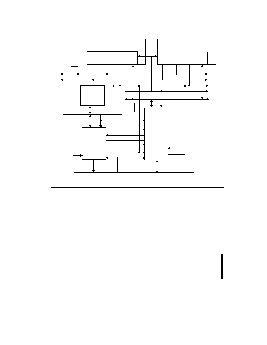
At the system level, APIC consists of two parts (Figure 2.0)--one residing in the I/O subsystem (called the
IOAPIC) and the other in the CPU (called the Local APIC). The local APIC and the IOAPIC communicate over a
dedicated APIC bus. The IOAPIC bus interface consists of two bi-directional data signals (APICD[1:0]) and a
clock input (APICCLK).
The CPU's Local APIC Unit contains the necessary intelligence to determine whether or not its processor should
accept interrupts broadcast on the APIC bus. The Local Unit also provides local pending of interrupts, nesting
and masking of interrupts, and handles all interactions with its local processor (e.g., the INTR/INTA/EOI
protocol). The Local Unit further provides inter-processor interrupts and a timer, to its local processor. The
register level interface of a processor to its local APIC is identical for every processor.
The IOAPIC Unit consists of a set of interrupt input signals, a 24-entry by 64-bit Interrupt Redirection Table,
programmable registers, and a message unit for sending and receiving APIC messages over the APIC bus. I/O
devices inject interrupts into the system by asserting one of the interrupt lines to the IOAPIC. The IOAPIC
selects the corresponding entry in the Redirection Table and uses the information in that entry to format an
interrupt request message. Each entry in the Redirection Table can be individually programmed to indicate
edge/level sensitive interrupt signals, the interrupt vector and priority, the destination processor, and how the
processor is selected (statically or dynamically). The information in the table is used to transmit a message to
other APIC units (via the APIC bus).
The IOAPIC contains a set of programmable registers. Two of the registers (I/O Register Select and I/O Window
Registers) are located in the CPU's memory space and are used to indirectly access the other APIC registers as
described in Section 3.0, Register Description. The Version Register provides the implementation version of the
IOAPIC. The IOAPIC ID Register is programmed with an ID value that serves as a physical name of the IOAPIC.
This ID is loaded into the ARB ID Register when the IOAPIC ID Register is written and is used during bus
arbitration.
NOTE
The interrupt number or the vector does not imply a particular priority for being sent. The IOAPIC continually
polls the 24 interrupts in a rotating fashion, one at a time. The pending interrupt polled first is the one sent.
82093AA (IOAPIC)
4
PRELIMINARY
Local APIC
LINTIN0
LINTIN1
SMI#
Processor
Local APIC
LINTIN0
LINTIN1
SMI#
Processor
LINTIN1
LINTIN0
NMI
RESET
RESET
APIC Bus
RESET
I/O APIC Unit
RESET
SMIOUT#
SMI
IRQ[1,2:7,8#,9:12,14,15]
INTR
INTIN23/SMI#
APICACK1#
APICREQ#
CS#
PIIX3
MIRQ[1:0]
PCI Bus
Host-to-PCI
Bridge
INTIN[2,13,22]
MIRQ[1:0]
ISA Bus
APICACK2#
APIC_SYS
Figure 2. I/O And Local APIC Units

82093AA (IOAPIC)
5
PRELIMINARY
2.0.
SIGNAL DESCRIPTION
This section contains a detailed description of each signal. The signals are arranged in function groups
according to their interface.
Note that the "#" symbol at the end of a signal name indicates that the active, or asserted state occurs when the
signal is at a low voltage level. When "#" is not present after the signal name, the signal is asserted when at the
high voltage level.
The terms' assertion and negation are used extensively. This is done to avoid confusion when working with a
mixture of `active-low' and `active-high' signals. The term assert, or assertion indicates that a signal is active,
independent of whether that level is represented by a high or low voltage. The term negate, or negation indicates
that a signal is inactive.
The following notations are used to describe the signal and type:
I
Input pin
O
Output pin
ST
Schmitt Trigger Input pin
OD
Open Drain Output pin. This requires a pull-up to the VCC of the processor core
I/OD
Bi-directional Input withOpen Drain Output pin.
I/O
Bi-directional Input/Output pin
2.1.
System Bus Signals
Signal Name
Type
Description
D[7:0]
I/O
DATA: D[7:0] contain the data when writing to or reading from internal IOAPIC
registers. These signals are outputs when reading data from the IOAPIC and
they are inputs when writing data to the IOAPIC. These signals are tri-stated
during reset.
D/I#
I
DATA/INDEX#: This input selects whether the I/O Register Select
(IOREGSEL) Register or I/O Window (IOWIN) Register is accessed. All
internal IOAPIC registers are accessed with an indexing scheme. When the
D/I# pin is low, the IOREGSEL Register is accessed. When the D/I# pin is
high, the data becomes available from the register pointed to by the index
register. Typically, this signal is connected to SA4 on the ISA bus (i.e.,
IOREGSEL Register is at 00h and IOWIN Register is at 10h).
A[1:0]
I
ADDRESS: The IOAPIC is a 32 bit device with an 8 bit ISA interface. A[1:0]
steer the data byte to the correct 8 bit location within the 32 bit register.
Typically, these input signals are connected to SA[1:0] of the ISA bus.
RD#
I
READ STROBE: RD# causes the IOAPIC to respond by driving internal
register data onto the D[7:0] pins. Typically this pin is connected to the
MEMRD# signal on the ISA bus.
WR#
I
WRITE STROBE: When this signal transitions from low to high, the data
present on the IOAPIC's D[7:0] signals are written to an internal register.
Typically, this signal is connected to the MEMWR# signal on the ISA bus.
CS#
I
CHIP SELECT: This active low input selects the IOAPIC as the target of the
current read or write transaction.